DATA SHEET
BIPOLAR ANALOG INTEGRATED CIRCUIT
μ PC29xxB Series
THREE-TERMINAL LOW DROPOUT VOLTAGE REGULATOR
(OUTPUT CURRENT: 1.0 A)
DESCRIPTION
The μ PC29xxB series is a series of three-terminal low dropout voltage regulators with 1.0 A output current. This
series is suitable for low voltage operated IC and has 4 output voltage types, 1.8 V, 2.5 V, 3.3 V and 5.0 V. Compared
with the μ PC29xx and μ PC29xxA series, this series has improved output voltage tolerance (VO ± 2%), quiescent
current (1.8 mA TYP. (IO = 0 A)), and short-circuit current.
FEATURES
• Output current capacity: 1.0 A
• Output voltage tolerance: VO ± 2% (TA = 25°C)
• Low quiescent current: 1.8 mA TYP. (IO = 0 A)
• Low short-circuit current: 0.3 A TYP. (μ PC2918B), 0.6 A TYP. (μ PC2925B, μ PC2933B), 0.65 A TYP. (μ PC2905B)
• Low dropout voltage: VDIF = 0.6 V MAX. (IO = 0.5 A)
• On-chip inrush current protection circuit at the time of input voltage rising (when input voltage is low)
• On-chip over-current limiter
• On-chip thermal shut down circuit
APPLICATIONS
Digital TV, DVD, LCD Monitors, Printers, Audio, Air Conditioners, and other applications.
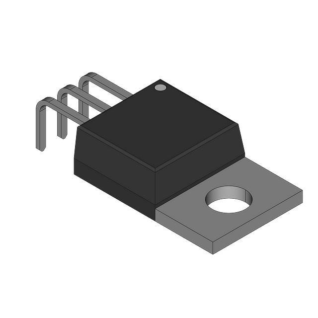
PIN CONFIGURATIONS (Marking Side)
Isolated TO-220 (MP-45G)
SC-64 (MP-3)
4
1
1
2
3
1: INPUT
2: GND
3: OUTPUT
2
TO-252 (MP-3ZK)
SC-63 (MP-3Z)
4
4
3
1
2
1: INPUT
Note1
2: GND
3: OUTPUT
4: GND (Fin)
1
3
1: INPUT
2: GND Note2
3: OUTPUT
4: GND (Fin)
2
3
1: INPUT
2: GND Note2
3: OUTPUT
4: GND (Fin)
Notes 1. No.2 pin and No.4 fin are common GND.
2. No.2 pin is cut. No.2 pin and No.4 fin are common GND.
The information in this document is subject to change without notice. Before using this document, please
confirm that this is the latest version.
Not all products and/or types are available in every country. Please check with an NEC Electronics
sales representative for availability and additional information.
Document No. G17567EJ4V0DS00 (4th edition)
Date Published August 2007 NS
Printed in Japan
2005, 2007
The mark shows major revised points.
The revised points can be easily searched by copying an "" in the PDF file and specifying it in the "Find what:" field.
�μ PC29xxB Series
BLOCK DIAGRAM
OUTPUT
Saturation protection
−
Overcurrent protection
Error
Amp.
Drive circuit
Reference voltage
+
Thermal shut down
Startup circuit
INPUT
GND
ORDERING INFORMATION
Part Number
Package
Output Voltage
Marking
μ PC2918BHF
Isolated TO-220 (MP-45G)
1.8 V
2918B
μ PC2918BHB
SC-64 (MP-3)
1.8 V
2918B
μ PC2918BT
SC-63 (MP-3Z)
1.8 V
2918B
μ PC2918BT1D
TO-252 (MP-3ZK)
1.8 V
2918BD
μ PC2925BHF
Isolated TO-220 (MP-45G)
2.5 V
2925B
μ PC2925BHB
SC-64 (MP-3)
2.5 V
2925B
μ PC2925BT
SC-63 (MP-3Z)
2.5 V
2925B
μ PC2925BT1D
TO-252 (MP-3ZK)
2.5 V
2925BD
μ PC2933BHF
Isolated TO-220 (MP-45G)
3.3 V
2933B
μ PC2933BHB
SC-64 (MP-3)
3.3 V
2933B
μ PC2933BT
SC-63 (MP-3Z)
3.3 V
2933B
μ PC2933BT1D
TO-252 (MP-3ZK)
3.3 V
2933BD
μ PC2905BHF
Isolated TO-220 (MP-45G)
5.0 V
2905B
μ PC2905BHB
SC-64 (MP-3)
5.0 V
2905B
μ PC2905BT
SC-63 (MP-3Z)
5.0 V
2905B
μ PC2905BT1D
TO-252 (MP-3ZK)
5.0 V
2905BD
Remark Tape-packaged products have the symbol -E1, or -E2 suffixed to the part number. In Pb-free products, any
of -AT, -AZ or -AY is added to the end of their part number. Refer to the following table for details.
2
Data Sheet G17567EJ4V0DS
�μ PC29xxB Series
Part Number
Note1
μ PC29xxBHF
μ PC29xxBHF-AZ
Note2
μ PC29xxBHB
Package
Package Type
Isolated TO-220 (MP-45G)
• Packed in envelop
Isolated TO-220 (MP-45G)
• Packed in envelop
SC-64 (MP-3)
• Packed in envelop
μ PC29xxBHB-AZ
Note2
SC-64 (MP-3)
• Packed in envelop
μ PC29xxBHB-AY
Note3
SC-64 (MP-3)
• Packed in envelop
SC-63 (MP-3Z)
• Packed in envelop
SC-63 (MP-3Z)
• Packed in envelop
SC-63 (MP-3Z)
• 16 mm wide embossed taping
μ PC29xxBT
μ PC29xxBT-AZ
Note2
μ PC29xxBT-E1
• Pin 1 on draw-out side
• 2000 pcs/reel
μ PC29xxBT-E1-AZ
Note2
SC-63 (MP-3Z)
• 16 mm wide embossed taping
• Pin 1 on draw-out side
• 2000 pcs/reel
μ PC29xxBT-E1-AY
Note3
SC-63 (MP-3Z)
• 16 mm wide embossed taping
• Pin 1 on draw-out side
• 2000 pcs/reel
μ PC29xxBT-E2
SC-63 (MP-3Z)
• 16 mm wide embossed taping
• Pin 1 at take-up side
• 2000 pcs/reel
μ PC29xxBT-E2-AZ
Note2
SC-63 (MP-3Z)
• 16 mm wide embossed taping
• Pin 1 at take-up side
• 2000 pcs/reel
μ PC29xxBT-E2-AY
Note3
SC-63 (MP-3Z)
• 16 mm wide embossed taping
• Pin 1 at take-up side
• 2000 pcs/reel
μ PC29xxBT1D-E1
TO-252 (MP-3ZK)
• 16 mm wide embossed taping
• Pin 1 on draw-out side
• 2500 pcs/reel
μ PC29xxBT1D-E1-AT
Note4
TO-252 (MP-3ZK)
• 16 mm wide embossed taping
• Pin 1 on draw-out side
• 2500 pcs/reel
μ PC29xxBT1D-E2
TO-252 (MP-3ZK)
• 16 mm wide embossed taping
• Pin 1 at take-up side
• 2500 pcs/reel
μ PC29xxBT1D-E2-AT
Note4
TO-252 (MP-3ZK)
• 16 mm wide embossed taping
• Pin 1 at take-up side
• 2500 pcs/reel
Notes 1. xx stands for symbols that indicate the output voltage.
2. Pb-free (This product does not contain Pb in the external electrode.)
3. Pb-free (This product does not contain Pb in the external electrode, Sn100% plating.)
4. Pb-free (This product does not contain Pb in the external electrode and other parts.)
Data Sheet G17567EJ4V0DS
3
�μ PC29xxB Series
ABSOLUTE MAXIMUM RATINGS (TA = 25°C, unless otherwise specified)
Parameter
Symbol
Rating
μ PC29xxBHF
Unit
μ PC29xxBHB,
μ PC29xxBT,
μ PC29xxBT1D
Input Voltage
−0.3 to +16.0
VIN
Internal Power Dissipation (TC = 25°C)
Note
PT
15
V
10
W
Operating Ambient Temperature
TA
−40 to +85
°C
Operating Junction Temperature
TJ
−40 to +150
°C
Storage Temperature
Tstg
−55 to +150
°C
Thermal Resistance (junction to case)
Rth(J-C)
7
12.5
°C/W
Thermal Resistance (junction to ambient)
Rth(J-A)
65
125
°C/W
Note Internally limited. When the operating junction temperature rises above 150°C, the internal circuit shuts down
the output voltage.
Caution Product quality may suffer if the absolute maximum rating is exceeded even momentarily for any
parameter. That is, the absolute maximum ratings are rated values at which the product is on the
verge of suffering physical damage, and therefore the product must be used under conditions that
ensure that the absolute maximum ratings are not exceeded.
TYPICAL CONNECTION
D1
μ PC29xxB
INPUT
OUTPUT
+
CIN
COUT
D2
CIN : 0.1 μ F or higher. Be sure to connect CIN to prevent parasitic oscillation. Set this value according to the length
of the line between the regulator and the INPUT pin. Use of a film capacitor or other capacitor with first-rate
voltage and temperature characteristics is recommended.
If using a laminated ceramic capacitor, it is
necessary to ensure that CIN is 0.1 μ F or higher for the voltage and temperature range to be used.
COUT: 10 μ F or higher. Be sure to connect COUT to prevent oscillation and improve excessive load regulation. Place
CIN and COUT as close as possible to the IC pins (within 1 to 2 cm). Also, use an electrolytic capacitor with low
impedance characteristics if considering use at sub-zero temperatures.
D1
: If the OUTPUT pin has a higher voltage than the INPUT pin, connect a diode.
D2
: If the OUTPUT pin has a lower voltage than the GND pin, connect a Schottky barrier diode.
Caution Make sure that no voltage is applied to the OUTPUT pin from external.
4
Data Sheet G17567EJ4V0DS
�μ PC29xxB Series
RECOMMENDED OPERATING CONDITIONS
Parameter
Input Voltage
Output Current
Symbol
Type Number
VIN
MIN.
TYP.
MAX.
Unit
μ PC2918B
2.8
12.0
V
μ PC2925B
3.5
12.0
V
μ PC2933B
4.3
12.0
V
μ PC2905B
6.0
12.0
V
IO
All
0
1.0
A
Operating Ambient Temperature TA
All
− 40
+ 85
°C
Operating Junction Temperature TJ
All
− 40
+ 125
°C
Caution Use of conditions exceeding the above-listed recommended operating conditions is not a problem
as long as the absolute maximum ratings are not exceeded.
However, since the use of such
conditions diminishes the margin of safety, careful evaluation is required before such conditions
are used.
ELECTRICAL CHARACTERISTICS
μ PC2918B (TJ = 25°C, VIN = 2.8 V, IO = 0.5 A, CIN = 0.1 μ F, COUT = 10 μ F, unless otherwise specified)
Parameter
Output Voltage
Symbol
Conditions
VO1
VO2
2.8 V ≤ VIN ≤ 12 V, 0 A ≤ IO ≤ 1 A
MIN.
TYP.
MAX.
Unit
1.764
1.8
1.836
V
(1.746)
−
(1.854)
V
Line Regulation
REGIN
2.8 V ≤ VIN ≤ 12 V
−
4.0
25.0
mV
Load Regulation
REGL
0 A ≤ IO ≤ 1 A
−
3.5
30.0
mV
Quiescent Current
IBIAS
IO = 0 A
−
1.8
4.0
mA
IO = 0.5 A
−
18.0
(30.0)
mA
Startup Quiescent Current
IBIAS(S)
VIN = 1.7 V, IO = 0 A
−
1.0
30.0
mA
VIN = 2.4 V, IO = 1 A
−
−
(80.0)
mA
Quiescent Current Change
ΔIBIAS
2.8 V ≤ VIN ≤ 12 V
−
(3.0)
(15.0)
mA
Output Noise Voltage
Vn
10 Hz ≤ f ≤ 100 kHz
−
50.0
−
μ Vr.m.s.
Ripple Rejection
R•R
f = 120 Hz, 2.8 V ≤ VIN ≤ 3.8 V, IO = 0.3 A
−
62
−
dB
Dropout Voltage
VDIF
IO = 0.5 A
−
0.3
0.6
V
IO = 1 A
−
(0.7)
−
V
(0.1)
0.3
(0.8)
A
VIN = 12 V
−
(0.4)
−
A
VIN = 2.8 V
1.0
1.3
(1.6)
A
VIN = 12 V
−
(1.1)
−
A
−
0.1
−
mV/°C
Short Circuit Current
IOshort
Peak Output Current
IOpeak
Temperature Coefficient of
Output Voltage
ΔVO/ΔT
VIN = 2.8 V
0°C ≤ TJ ≤ 125°C, IO = 5 mA
Remark Values in parentheses are product design values, and are thus provided as reference values.
Data Sheet G17567EJ4V0DS
5
�μ PC29xxB Series
μ PC2925B (TJ = 25°C, VIN = 3.5 V, IO = 0.5 A, CIN = 0.1 μ F, COUT = 10 μ F, unless otherwise specified)
Parameter
Symbol
Conditions
MIN.
TYP.
MAX.
Unit
2.45
2.5
2.55
V
(2.425)
−
(2.575)
V
−
5.5
25.0
mV
0 A ≤ IO ≤ 1 A
−
3.5
40.0
mV
Output Voltage
VO1
VO2
3.5 V ≤ VIN ≤ 12 V, 0 A ≤ IO ≤ 1 A
Line Regulation
REGIN
3.5 V ≤ VIN ≤ 12 V
Load Regulation
REGL
Quiescent Current
IBIAS
IO = 0 A
−
1.8
4.0
mA
IO = 0.5 A
−
18.0
(30.0)
mA
VIN = 2.4 V, IO = 0 A
−
11.0
30.0
mA
mA
Startup Quiescent Current
IBIAS(S)
VIN = 3.1 V, IO = 1 A
−
−
(80.0)
Quiescent Current Change
ΔIBIAS
3.5 V ≤ VIN ≤ 12 V
−
(3.0)
(15.0)
mA
Output Noise Voltage
Vn
10 Hz ≤ f ≤ 100 kHz
−
62.0
−
μ Vr.m.s.
Ripple Rejection
R•R
f = 120 Hz, 3.5 V ≤ VIN ≤ 4.5 V, IO = 0.3 A
−
60
−
dB
Dropout Voltage
VDIF
IO = 0.5 A
−
0.36
0.6
V
IO = 1 A
−
(0.7)
−
V
A
Short Circuit Current
IOshort
Peak Output Current
IOpeak
Temperature Coefficient of
Output Voltage
ΔVO/ΔT
VIN = 3.5 V
(0.1)
0.6
(0.8)
VIN = 12 V
−
(0.4)
−
A
VIN = 3.5 V
1.0
1.3
(1.6)
A
VIN = 12 V
−
(1.1)
−
A
−
0.2
−
mV/°C
0°C ≤ TJ ≤ 125°C, IO = 5 mA
Remark Values in parentheses are product design values, and are thus provided as reference values.
μ PC2933B (TJ = 25°C, VIN = 5.0 V, IO = 0.5 A, CIN = 0.1 μ F, COUT = 10 μ F, unless otherwise specified)
Parameter
Output Voltage
Symbol
Conditions
VO1
TYP.
MAX.
Unit
V
3.234
3.3
3.366
(3.201)
−
(3.399)
V
4.3 V ≤ VIN ≤ 12 V
−
6.0
25.0
mV
REGL
0 A ≤ IO ≤ 1 A
−
4.2
50.0
mV
IBIAS
IO = 0 A
−
1.8
4.0
mA
IO = 0.5 A
−
18.0
(30.0)
mA
VIN = 3.1 V, IO = 0 A
−
11.0
30.0
mA
VIN = 3.7 V, IO = 1 A
−
−
(80.0)
mA
VO2
4.3 V ≤ VIN ≤ 12 V, 0 A ≤ IO ≤ 1 A
Line Regulation
REGIN
Load Regulation
Quiescent Current
Startup Quiescent Current
MIN.
IBIAS(S)
Quiescent Current Change
ΔIBIAS
4.3 V ≤ VIN ≤ 12 V
−
(3.0)
(15.0)
mA
Output Noise Voltage
Vn
10 Hz ≤ f ≤ 100 kHz
−
82.0
−
μ Vr.m.s.
Ripple Rejection
R•R
f = 120 Hz, 4.3 V ≤ VIN ≤ 5.3 V, IO = 0.3 A
−
58
−
dB
Dropout Voltage
VDIF
IO = 0.5 A
−
0.36
0.6
V
IO = 1 A
−
(0.7)
−
V
(0.1)
0.6
(0.8)
A
VIN = 12 V
−
(0.4)
−
A
VIN = 5.0 V
1.0
1.5
(1.6)
A
VIN = 12 V
−
(1.1)
−
A
−
0.4
−
mV/°C
Short Circuit Current
IOshort
Peak Output Current
IOpeak
Temperature Coefficient of
Output Voltage
ΔVO/ΔT
VIN = 5.0 V
0°C ≤ TJ ≤ 125°C, IO = 5 mA
Remark Values in parentheses are product design values, and are thus provided as reference values.
6
Data Sheet G17567EJ4V0DS
�μ PC29xxB Series
μ PC2905B (TJ = 25°C, VIN = 6.0 V, IO = 0.5 A, CIN = 0.1 μ F, COUT = 10 μ F, unless otherwise specified)
Parameter
Symbol
Conditions
MIN.
TYP.
MAX.
Unit
4.90
5.0
5.10
V
(4.85)
−
(5.15)
V
−
6.5
25.0
mV
0 A ≤ IO ≤ 1 A
−
5.0
80.0
mV
Output Voltage
VO1
VO2
6.0 V ≤ VIN ≤ 12 V, 0 A ≤ IO ≤ 1 A
Line Regulation
REGIN
6.0 V ≤ VIN ≤ 12 V
Load Regulation
REGL
Quiescent Current
IBIAS
IO = 0 A
−
1.8
4.0
mA
IO = 0.5 A
−
18.0
(30.0)
mA
VIN = 4.8 V, IO = 0 A
−
11.0
30.0
mA
mA
Startup Quiescent Current
IBIAS(S)
VIN = 5.5 V, IO = 1 A
−
−
(80.0)
Quiescent Current Change
ΔIBIAS
6.0 V ≤ VIN ≤ 12 V
−
(3.0)
(15.0)
mA
Output Noise Voltage
Vn
10 Hz ≤ f ≤ 100 kHz
−
122.0
−
μ Vr.m.s.
Ripple Rejection
R•R
f = 120 Hz, 6.0 V ≤ VIN ≤ 7 V, IO = 0.3 A
−
57
−
dB
Dropout Voltage
VDIF
IO = 0.5 A
−
0.38
0.6
V
IO = 1 A
−
(0.7)
−
V
A
Short Circuit Current
IOshort
Peak Output Current
IOpeak
Temperature Coefficient of
Output Voltage
ΔVO/ΔT
VIN = 6.5 V
(0.1)
0.65
(0.8)
VIN = 12 V
−
(0.4)
−
A
VIN = 6.5 V
1.0
1.5
(1.6)
A
VIN = 12 V
−
(1.1)
−
A
−
0.6
−
mV/°C
0°C ≤ TJ ≤ 125°C, IO = 5 mA
Remark Values in parentheses are product design values, and are thus provided as reference values.
Data Sheet G17567EJ4V0DS
7
�μ PC29xxB Series
TYPICAL CHARACTERISTICS (TA = 25°C)
Δ VO vs.TJ
Pd vs. TA
Solid line: m PC29xxBHF
Broken line: m PC29xxBT1D,
m PC29xxBT,
m PC29xxBHB
W
ith
in
fin
ite
he
at
sin
k
15
10
Δ VO - Output Voltage Change - mV
Pd - Total Power Dissipation - W
20
100
5
Without he
atsink
1.92
1.0
0
IO = 5 mA
80
60
40
20
0
-20
μ PC2918B (VIN = 2.8 V)
μ PC2925B (VIN = 3.5 V)
μ PC2933B (VIN = 5.0 V)
μ PC2905B (VIN = 6.0 V)
-40
-60
-80
-100
50
0
85 100
150
-50
-25
0
25
50
75
TJ - Operating Junction Temperature - °C
TA - Operating Ambient Temperature - °C
VO vs. VIN (μ PC2918B)
VO vs. VIN (μ PC2925B)
2.5
3
TJ = 25°C
2.5
2
VO - Output Voltage - V
VO - Output Voltage - V
TJ = 25°C
1.5
IO = 5 mA
IO = 0.5 A
IO = 1 A
1
0.5
1.5
1
0.5
0
0
2
4
6
8
0
2
4
6
VIN - Input Voltage - V
VIN - Input Voltage - V
VO vs. VIN (μ PC2933B)
VO vs. VIN (μ PC2905B)
8
6
4
TJ = 25°C
3.5
TJ = 25°C
5
VO - Output Voltage - V
VO - Output Voltage - V
IO = 5 mA
IO = 0.5 A
IO = 1 A
2
0
3
IO = 5 mA
IO = 0.5 A
IO = 1 A
2.5
2
1.5
1
0.5
4
IO = 5 mA
IO = 0.5 A
IO = 1 A
3
2
1
0
0
0
2
4
6
8
0
2
4
6
VIN - Input Voltage - V
VIN - Input Voltage - V
8
100 125
Data Sheet G17567EJ4V0DS
8
�μ PC29xxB Series
IBIAS (IBIAS(s)) vs. VIN (μ PC2925B)
80
80
70
70
IBIAS - Quiescent Current - mA
IBIAS - Quiescent Current - mA
IBIAS (IBIAS(s)) vs. VIN (μ PC2918B)
60
50
40
IO = 1 A
30
20
IO = 0.5 A
10
IO = 5 mA
60
50
40
IO = 1 A
30
20
IO = 0.5 A
10
IO = 5 mA
0
0
0
2
4
6
8
10
12
14
0
16
2
4
80
80
70
70
60
50
IO = 1 A
30
IO = 0.5 A
IO = 5 mA
10
12
14
16
60
50
IO = 1 A
40
30
IO = 0.5 A
20
IO = 5 mA
10
0
0
0
2
4
6
8
10
12
14
16
0
2
4
6
8
10
12
VIN - Input Voltage - V
VIN - Input Voltage - V
VDIF vs. TJ
IOpeak vs. VDIF
1
14
16
2
IOpeak - Peak Output Current - A
IO = 0.5 A
0.9
VDIF - Dropout Voltage - V
10
IBIAS (IBIAS(s)) vs. VIN (μ PC2905B)
IBIAS - Quiescent Current - mA
IBIAS - Quiescent Current - mA
IBIAS (IBIAS(s)) vs. VIN (μ PC2933B)
20
8
VIN - Input Voltage - V
VIN - Input Voltage - V
40
6
0.8
μ PC2933B
0.7
0.6
μ PC2905B
0.5
0.4
0.3
μ PC2925B
0.2
μ PC2918B
0.1
μ PC2925B
μ PC2905B
1.5
1
μ PC2933B
μ PC2918B
0.5
TJ = 25°C
0
0
-50 -25
0
25
50
75
100 125 150
TJ - Operating Junction Temperature - °C
Data Sheet G17567EJ4V0DS
0
3
6
9
12
15
VDIF - Dropout Voltage - V
9
�μ PC29xxB Series
R•R vs. f (μ PC2918B)
70
R•R - Ripple Rejection - dB
80
IO = 5 mA
60
IO = 0.3 A
IO = 0.5 A
50
IO = 1 A
40
30
20
TJ = 25°C
VIN = 2.8 V
10
R•R - Ripple Rejection - dB
80
R•R vs. f (μ PC2925B)
0
100
1000
10000
50
30
20
10
1000
10000
100000
80
IO = 5 mA
IO = 1 A
30
20
TJ = 25°C
VIN = 5.0 V
R•R - Ripple Rejection - dB
IO = 0.5 A
10
IO = 5 mA
70
IO = 0.3 A
0
IO = 0.3 A
60
50
40
IO = 0.5 A
IO = 1 A
30
20
TJ = 25°C
VIN = 6.0 V
10
0
10
100
1000
10000
100000
10
100
1000
10000
100000
f - Frequency - Hz
f - Frequency - Hz
VO vs. IO (μ PC2918B)
VDIF vs. IO
1
3.0
TJ = 25°C
0.9
VIN = 2.8 V
2.5
μ PC2933B
VO - Output Voltage - V
VDIF - Dropout Voltage - V
100
R•R vs. f (μ PC2905B)
40
μ PC2925B
μ PC2905B
0.4
0.3
0.2
TJ = 25°C
VIN = 3.5 V
10
R•R vs. f (μ PC2933B)
50
0.5
IO = 1 A
f - Frequency - Hz
60
0.6
IO = 0.5 A
40
f - Frequency - Hz
70
R•R - Ripple Rejection - dB
60
100000
80
0.7
IO = 0.3 A
0
10
0.8
IO = 5 mA
70
μ PC2918B
2.0
1.5
1.0
0.5
0.1
0
0
10
0 0.1 0.2 0.3 0.4 0.5 0.6 0.7 0.8 0.9 1
0 0.2 0.4 0.6 0.8 1.0 1.2 1.4 1.6 1.8 2.0
IO - Output Current - A
IO - Output Current - A
Data Sheet G17567EJ4V0DS
�μ PC29xxB Series
VO vs. IO (μ PC2925B)
VO vs. IO (μ PC2933B)
3.0
5.0
VIN = 3.5 V
VIN = 5.0 V
4.0
VO - Output Voltage - V
VO - Output Voltage - V
2.5
2.0
1.5
1.0
0.5
0
3.0
2.0
1.0
0.2 0.4 0.6 0.8 1.0 1.2 1.4 1.6 1.8 2.0
IO - Output Current - A
0
0.2 0.4 0.6 0.8 1.0 1.2 1.4 1.6 1.8 2.0
IO - Output Current - A
VO vs. IO (μ PC2905B)
6.0
VIN = 6.5 V
VO - Output Voltage - V
5.0
4.0
3.0
2.0
1.0
0
0.2 0.4 0.6 0.8 1.0 1.2 1.4 1.6 1.8 2.0
IO - Output Current - A
Data Sheet G17567EJ4V0DS
11
�μ PC29xxB Series
PACKAGE DRAWINGS (Unit: mm)
μ PC2918BHF, μ PC2925BHF, μ PC2933BHF, μ PC2905BHF
3PIN PLASTIC SIP (MP-45G)
A
N
E
P
B
I
L
M
D
1
2
3
K
Y
V
J
H
U
Z
C
F
G
M
NOTE
ITEM
Each lead centerline is located within 0.25 mm of
its true position (T.P.) at maximum material condition.
MILLIMETERS
A
10.0±0.2
B
7.0±0.2
C
1.50±0.2
D
E
17.0±0.3
φ 3.3±0.2
F
0.75±0.10
G
0.25
H
2.54 (T.P.)
I
5.0±0.3
J
K
2.46±0.2
5.0±0.2
L
8.5±0.2
M
8.5±0.2
N
4.5±0.2
P
U
V
2.8±0.2
2.4±0.5
0.65±0.10
Y
Z
8.9±0.7
1.30±0.2
P3HF-254B-4
12
Data Sheet G17567EJ4V0DS
�μ PC29xxB Series
μ PC2918BHB, μ PC2925BHB, μ PC2933BHB, μ PC2905BHB
SC-64 (MP-3)
2.3±0.2
1.5 +0.2
−0.1
6.5±0.2
5.0±0.2
0.5±0.1
2
3
7.0 MIN.
1
13.7 MIN.
1.6±0.2
5.5±0.2
4
1.1±0.1
0.5 +0.2
−0.1
2.3
0.75
2.3
0.5 +0.2
−0.1
μ PC2918BT, μ PC2925BT, μ PC2933BT, μ PC2905BT
SC-63 (MP-3Z) (Unit: mm)
6.5±0.2
2.3±0.2
4.4±0.2
1.5 −0.1
+0.2
5.0±0.2
Note
0.5±0.1
2
3
2.5±0.5
1.0±0.5
0.4 MIN.
0.5 TYP.
1
9.5±0.5
4
5.6±0.3
Note
5.5±0.2
0.5±0.1
0.5±0.1
2.3±0.3
2.3±0.3
0.15±0.15
Note The depth of notch at the top of the fin is from 0 to 0.2 mm.
Data Sheet G17567EJ4V0DS
13
�μ PC29xxB Series
μ PC2918BT1D, μ PC2925BT1D, μ PC2933BT1D, μ PC2905BT1D
TO-252 (MP-3ZK)
1.0 TYP.
6.5±0.2
5.1 TYP.
4.3 MIN.
2.3±0.1
0.5±0.1
1.14 MAX.
3
0.51 MIN.
2
0.8
1
6.1±0.2
10.4 MAX. (9.8 TYP.)
4.0 MIN.
4
0 to 0.25
0.5±0.1
0.76±0.12
2.3
2.3
1.0
14
Data Sheet G17567EJ4V0DS
�μ PC29xxB Series
RECOMMENDED MOUNTING CONDITIONS
The μ PC29xxB Series should be soldered and mounted under the following recommended conditions.
For soldering methods and conditions other than those recommended below, contact an NEC Electronics sales
representative.
For technical information, see the following website.
Semiconductor Device Mount Manual (http://www.necel.com/pkg/en/mount/index.html)
Surface Mount Device
μ PC29xxBT Series: SC-63 (MP-3Z)
μ PC29xxBT1D Series: TO-252 (MP-3ZK)
Process
Infrared Ray Reflow
Conditions
Peak temperature: 260°C or below (Package surface temperature),
Symbol
IR60-00-3
Reflow time: 60 seconds or less (at 220°C or higher),
Maximum number of reflow processes: 3 times or less.
Vapor Phase Soldering
Peak temperature: 215°C or below (Package surface temperature),
VP15-00-3
Reflow time: 40 seconds or less (at 200°C or higher),
Maximum number of reflow processes: 3 times or less.
Partial Heating Method
Pin temperature: 350°C or below,
P350
Heat time: 3 seconds or less (Per each side of the device).
Note1
μ PC29xxBT-AZ Series
, μ PC29xxBT-AY Series
Note3
μ PC29xxBT1D-AT Series
: TO-252 (MP-3ZK)
Note2
Process
Infrared Ray Reflow
: SC-63 (MP-3Z)
Conditions
Peak temperature: 260°C or below (package surface temperature),
Symbol
IR60-00-3
Reflow time: 60 seconds or less (at 220°C or higher),
Maximum number of reflows processes: 3 times or less.
Partial Heating Method
Pin temperature: 350°C or below,
P350
Heat time: 3 seconds or less (per each side of the device).
Notes 1. Pb-free (This product does not contain Pb in the external electrode.)
2. Pb-free (This product does not contain Pb in the external electrode, Sn100% plating.)
3. Pb-free (This product does not contain Pb in the external electrode and other parts.)
Caution Apply only one kind of soldering condition to a device, except for "partial heating method", or the device
will be damaged by heat stress.
Remark Flux: Rosin-based flux with low chlorine content (chlorine 0.2 Wt% or below) is recommended.
Data Sheet G17567EJ4V0DS
15
�μ PC29xxB Series
Type of Through-hole Device
Note1
μ PC29xxBHF Series, μ PC29xxBHF-AZ Series
: Isolated TO-220 (MP-45G)
Note1
Note2
μ PC29xxBHB Series, μ PC29xxBHB-AZ Series
, μ PC29xxBHB-AY Series
: SC-64 (MP-3)
Process
Wave Soldering
Conditions
Symbol
Solder temperature: 260°C or below, Flow time: 10 seconds or less
WS60-00-1
(only to leads)
Partial Heating Method
Pin temperature: 350°C or below, Heat time: 3 seconds or less (per each pin).
P350
Notes 1. Pb-free (This product does not contain Pb in the external electrode.)
2. Pb-free (This product does not contain Pb in the external electrode, Sn100% plating.)
Caution For through-hole device, the wave soldering process must be applied only to leads, and make sure
that the package body does not get jet soldered.
REFERENCE DOCUMENTS
USER’S MANUAL USAGE OF THREE TERMINAL REGULATORS
Document No.G12702E
REVIEW OF QUALITY AND RELIABILITY HANDBOOK
Document No.C12769E
INFORMATION VOLTAGE REGULATOR OF SMD
Document No.G11872E
SEMICONDUCTOR DEVICE MOUNT MANUAL
http://www.necel.com/pkg/en/mount/index.html
16
Data Sheet G17567EJ4V0DS
�μ PC29xxB Series
• The information in this document is current as of August, 2007. The information is subject to
change without notice. For actual design-in, refer to the latest publications of NEC Electronics data
sheets or data books, etc., for the most up-to-date specifications of NEC Electronics products. Not
all products and/or types are available in every country. Please check with an NEC Electronics sales
representative for availability and additional information.
• No part of this document may be copied or reproduced in any form or by any means without the prior
written consent of NEC Electronics. NEC Electronics assumes no responsibility for any errors that may
appear in this document.
• NEC Electronics does not assume any liability for infringement of patents, copyrights or other intellectual
property rights of third parties by or arising from the use of NEC Electronics products listed in this document
or any other liability arising from the use of such products. No license, express, implied or otherwise, is
granted under any patents, copyrights or other intellectual property rights of NEC Electronics or others.
• Descriptions of circuits, software and other related information in this document are provided for illustrative
purposes in semiconductor product operation and application examples. The incorporation of these
circuits, software and information in the design of a customer's equipment shall be done under the full
responsibility of the customer. NEC Electronics assumes no responsibility for any losses incurred by
customers or third parties arising from the use of these circuits, software and information.
• While NEC Electronics endeavors to enhance the quality, reliability and safety of NEC Electronics products,
customers agree and acknowledge that the possibility of defects thereof cannot be eliminated entirely. To
minimize risks of damage to property or injury (including death) to persons arising from defects in NEC
Electronics products, customers must incorporate sufficient safety measures in their design, such as
redundancy, fire-containment and anti-failure features.
• NEC Electronics products are classified into the following three quality grades: "Standard", "Special" and
"Specific".
The "Specific" quality grade applies only to NEC Electronics products developed based on a customerdesignated "quality assurance program" for a specific application. The recommended applications of an NEC
Electronics product depend on its quality grade, as indicated below. Customers must check the quality grade of
each NEC Electronics product before using it in a particular application.
"Standard": Computers, office equipment, communications equipment, test and measurement equipment, audio
and visual equipment, home electronic appliances, machine tools, personal electronic equipment
and industrial robots.
"Special": Transportation equipment (automobiles, trains, ships, etc.), traffic control systems, anti-disaster
systems, anti-crime systems, safety equipment and medical equipment (not specifically designed
for life support).
"Specific": Aircraft, aerospace equipment, submersible repeaters, nuclear reactor control systems, life
support systems and medical equipment for life support, etc.
The quality grade of NEC Electronics products is "Standard" unless otherwise expressly specified in NEC
Electronics data sheets or data books, etc. If customers wish to use NEC Electronics products in applications
not intended by NEC Electronics, they must contact an NEC Electronics sales representative in advance to
determine NEC Electronics' willingness to support a given application.
(Note)
(1) "NEC Electronics" as used in this statement means NEC Electronics Corporation and also includes its
majority-owned subsidiaries.
(2) "NEC Electronics products" means any product developed or manufactured by or for NEC Electronics (as
defined above).
M8E 02. 11-1
�