To our customers,
Old Company Name in Catalogs and Other Documents
On April 1st, 2010, NEC Electronics Corporation merged with Renesas Technology
Corporation, and Renesas Electronics Corporation took over all the business of both
companies. Therefore, although the old company name remains in this document, it is a valid
Renesas Electronics document. We appreciate your understanding.
Renesas Electronics website: http://www.renesas.com
April 1st, 2010
Renesas Electronics Corporation
Issued by: Renesas Electronics Corporation (http://www.renesas.com)
Send any inquiries to http://www.renesas.com/inquiry.
�Notice
1.
2.
3.
4.
5.
6.
7.
All information included in this document is current as of the date this document is issued. Such information, however, is
subject to change without any prior notice. Before purchasing or using any Renesas Electronics products listed herein, please
confirm the latest product information with a Renesas Electronics sales office. Also, please pay regular and careful attention to
additional and different information to be disclosed by Renesas Electronics such as that disclosed through our website.
Renesas Electronics does not assume any liability for infringement of patents, copyrights, or other intellectual property rights
of third parties by or arising from the use of Renesas Electronics products or technical information described in this document.
No license, express, implied or otherwise, is granted hereby under any patents, copyrights or other intellectual property rights
of Renesas Electronics or others.
You should not alter, modify, copy, or otherwise misappropriate any Renesas Electronics product, whether in whole or in part.
Descriptions of circuits, software and other related information in this document are provided only to illustrate the operation of
semiconductor products and application examples. You are fully responsible for the incorporation of these circuits, software,
and information in the design of your equipment. Renesas Electronics assumes no responsibility for any losses incurred by
you or third parties arising from the use of these circuits, software, or information.
When exporting the products or technology described in this document, you should comply with the applicable export control
laws and regulations and follow the procedures required by such laws and regulations. You should not use Renesas
Electronics products or the technology described in this document for any purpose relating to military applications or use by
the military, including but not limited to the development of weapons of mass destruction. Renesas Electronics products and
technology may not be used for or incorporated into any products or systems whose manufacture, use, or sale is prohibited
under any applicable domestic or foreign laws or regulations.
Renesas Electronics has used reasonable care in preparing the information included in this document, but Renesas Electronics
does not warrant that such information is error free. Renesas Electronics assumes no liability whatsoever for any damages
incurred by you resulting from errors in or omissions from the information included herein.
Renesas Electronics products are classified according to the following three quality grades: “Standard”, “High Quality”, and
“Specific”. The recommended applications for each Renesas Electronics product depends on the product’s quality grade, as
indicated below. You must check the quality grade of each Renesas Electronics product before using it in a particular
application. You may not use any Renesas Electronics product for any application categorized as “Specific” without the prior
written consent of Renesas Electronics. Further, you may not use any Renesas Electronics product for any application for
which it is not intended without the prior written consent of Renesas Electronics. Renesas Electronics shall not be in any way
liable for any damages or losses incurred by you or third parties arising from the use of any Renesas Electronics product for an
application categorized as “Specific” or for which the product is not intended where you have failed to obtain the prior written
consent of Renesas Electronics. The quality grade of each Renesas Electronics product is “Standard” unless otherwise
expressly specified in a Renesas Electronics data sheets or data books, etc.
Computers; office equipment; communications equipment; test and measurement equipment; audio and visual
equipment; home electronic appliances; machine tools; personal electronic equipment; and industrial robots.
“High Quality”: Transportation equipment (automobiles, trains, ships, etc.); traffic control systems; anti-disaster systems; anticrime systems; safety equipment; and medical equipment not specifically designed for life support.
“Specific”:
Aircraft; aerospace equipment; submersible repeaters; nuclear reactor control systems; medical equipment or
systems for life support (e.g. artificial life support devices or systems), surgical implantations, or healthcare
intervention (e.g. excision, etc.), and any other applications or purposes that pose a direct threat to human life.
You should use the Renesas Electronics products described in this document within the range specified by Renesas Electronics,
especially with respect to the maximum rating, operating supply voltage range, movement power voltage range, heat radiation
characteristics, installation and other product characteristics. Renesas Electronics shall have no liability for malfunctions or
damages arising out of the use of Renesas Electronics products beyond such specified ranges.
Although Renesas Electronics endeavors to improve the quality and reliability of its products, semiconductor products have
specific characteristics such as the occurrence of failure at a certain rate and malfunctions under certain use conditions. Further,
Renesas Electronics products are not subject to radiation resistance design. Please be sure to implement safety measures to
guard them against the possibility of physical injury, and injury or damage caused by fire in the event of the failure of a
Renesas Electronics product, such as safety design for hardware and software including but not limited to redundancy, fire
control and malfunction prevention, appropriate treatment for aging degradation or any other appropriate measures. Because
the evaluation of microcomputer software alone is very difficult, please evaluate the safety of the final products or system
manufactured by you.
Please contact a Renesas Electronics sales office for details as to environmental matters such as the environmental
compatibility of each Renesas Electronics product. Please use Renesas Electronics products in compliance with all applicable
laws and regulations that regulate the inclusion or use of controlled substances, including without limitation, the EU RoHS
Directive. Renesas Electronics assumes no liability for damages or losses occurring as a result of your noncompliance with
applicable laws and regulations.
This document may not be reproduced or duplicated, in any form, in whole or in part, without prior written consent of Renesas
Electronics.
Please contact a Renesas Electronics sales office if you have any questions regarding the information contained in this
document or Renesas Electronics products, or if you have any other inquiries.
“Standard”:
8.
9.
10.
11.
12.
(Note 1) “Renesas Electronics” as used in this document means Renesas Electronics Corporation and also includes its majorityowned subsidiaries.
(Note 2) “Renesas Electronics product(s)” means any product developed or manufactured by or for Renesas Electronics.
�DATA SHEET
MOS INTEGRATED CIRCUIT
μ PD166009
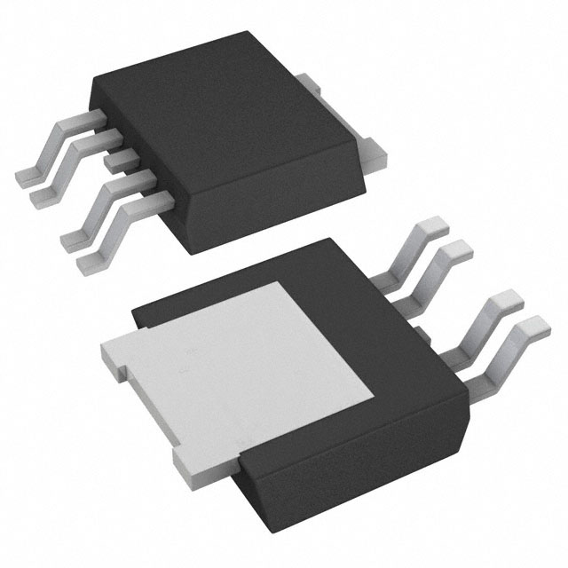
SINGLE N-CHANNEL HIGH SIDE INTELLIGENT POWER DEVICE
PACKAGE DRAWING (unit: mm)
The μ PD166009 device is an N-channel high-side switch with charge
4.0 MIN (4.4 TYP)
sense and embedded protection functions.
• Built-in charge pump
1
• Low on-state resistance
0.5±0.1
2
3
4
5
0 to 0.25
0.6±0.1
1.14
0.5±0.1
0.508
GAUGE PLANE
• Over-temperature protection
- Shutdown with auto-restart on cooling
SEATING PLANE
- Shutdown by short-circuit detection
1.52±0.12
0.8
• Short-circuit protection
2.3±0.1
6
6.1±0.2
FEATURES
1.0 TYP
6.5±0.2
5.0 TYP
4.3 MIN
pump, current controlled input, diagnostic feedback with load current
10.3 MAX (9.8 TYP)
GENERAL DESCRIPTION
• Small multi-chip package: JEDEC 5-pin TO-252
NOTE
1.
(MSL: 3, profile acc. J-STD-20C)
No Plating area
• Built-in diagnostic function
- Proportional load current sensing
- Defined fault signal in case of thermal shutdown and/or short circuit shutdown
•
AEC Qualified
ORDERING INFORMATION
Part Number
μ PD166009T1F-E1-AY
Note
Lead plating
Packing
Package
Sn
Tape 2500 p/reel
5-pin TO-252 (MP-3ZK)
Note Pb-free (This product does not contain Pb in the external electrode.)
QUALITY GRADE
Part Number
Quality Grade
μ PD166009T1F-E1-AY
Special
Please refer to "Quality Grades on NEC Semiconductor Devices" (Document No. C11531E) published by
NEC Corporation to know the specification of quality grade on the devices and its recommended applications.
APPLICATION
• Light bulb (to 55 W) switching
• Switching of all types of 14 V DC grounded loads, such as inductor, resistor and capacitor
• Replacement for fuse and relay
The information in this document is subject to change without notice. Before using this document, please confirm that this is the
latest version. Not all products and/or types are available in every country. Please check with an NEC Electronics sales
representative for availability and additional information.
Document No. S19688EJ2V0DS00 (2nd edition)
Date Published January 2010 NS
Printed in Japan
The mark shows major revised points.
The revised points can be easily searched by copying an "" in the PDF file and specifying it in the "Find what:" field.
2009
�μ PD166009
BLOCK DIAGRAM
3 & Tab
ICC
VCC
VCC - VIN
IIN
IN
2
VIN
Internal
power supply
Charge pump
Power supply
voltage sense
Current
detector
Dynamic
clamp
Output voltage
sense
Current sense
ESD
protection
Control logic
VCC
Von
ESD
protection
Fault signal
output
VOUT
4
Tab
Terminal Name
1
OUT
Output to load: pin 1 and 5 must be externally shorted.
2
IN
Input; activates the power switch, if shorted to ground.
3&Tab
VCC
Supply Voltage: tab and pin 3 are internally shorted.
OUT
IS
VIS
Pin No.
5
Load
IIS
RIS
PIN CONFIGURATION
IS
IL
OUT
Temperature
Sensor
4
1&5
Function
Sense Output: diagnostic feedback
1 2 3 4 5
Note
Output to load: pin 1 and 5 must be externally shorted.
Note If current sense and diagnostic features are not used, IS terminal has to be connected to GND via resistor.
2
Data Sheet S19688EJ2V0DS
�μ PD166009
ABSOLUTE MAXIMUM RATING (Ta = 25°C, unless otherwise specified)
Parameter
Symbol
VCC voltage
VCC1
VCC voltage (Load Dump)
VCC2
Test Conditions
Rating
Unit
28
V
40
V
RI = 1 Ω, RL = 1.5 Ω, td = 400 ms,
RIS = 1 kΩ, IN = low or high
VCC voltage (Reverse polarity)
-VCC
RL = 2.2 Ω, 1 minute
−16
V
Load current
IL
DC, TC = 25°C
30
A
Load current (short circuit
IL(SC)
Self Limited
A
TC = 25°C
59
W
Inductive load switch-off energy EAS1
IL = 10 A, VCC = 12 V, Tch,start ≤ 150°C,
50
mJ
dissipation single pulse
refer to page 16
105
mJ
current)
Power dissipation
Maximum allowable energy
PD
EAS2
VCC = 18 V, Tch,start ≤ 150°C, Rsupply = 10 mΩ,
Rshort = 50 mΩ, Lsupply = 5 μH, Lshort = 15 μH,
under over load condition
(Single pulse)
refer to page 16
Channel temperature
Tch
−40 to +150
°C
Storage temperature
Tstg
−55 to +150
°C
Electric discharge capability
VESD
2000
V
400
V
DC
VCC−28 V
V
Reverse polarity condition, 1 minute
VCC+14 V
V
DC
VCC−28 V
V
Reverse polarity condition, 1 minute
VCC+14 V
V
HBM
AEC-Q100-002 std.
R = 1.5 kΩ, C = 100pF
MM
AEC-Q100-003 std.
R = 0 Ω, C = 200pF
Voltage of IN pin
Voltage of IS pin
VIN
VIS
RECOMMENDED OPERATING CONDITIONS
Parameter
Power supply voltage
Symbol
VCC
Test Conditions
Tch = −40 to 150°C
Min.
Typ.
Max.
Unit
8
−
18
V
Cautions 1. It is assumed that VIN = 0 V when the device is activated.
2. Device operating range is limited by energy dissipation capability of the driver.
User must
carefully consider worst case load and current conditions in combination of operating voltage.
THERMAL CHARACTERISTICS
Parameter
Thermal resistance
Symbol
Rth(ch-a)
Test Conditions
Device on 50 mm x 50 mm x 1.5 mmt
Min.
Typ.
Max.
Unit
−
45
55
°C/W
−
−
3.17
°C/W
epoxy PCB FR-4 with 6 cm of 70 μm
2
copper area
Rth(ch-c)
Data Sheet S19688EJ2V0DS
3
�μ PD166009
ELECTRICAL CHARACTERISTICS (VCC = 12 V, Tch = 25°C, unless otherwise specified)
Parameter
Required current capability of
Symbol
IIH
Test Conditions
Min.
Typ.
Max.
Unit
−
1.0
2.2
mA
−
−
50
μA
Tch = 25°C
−
2.5
5.0
μA
Tch = −40 to 150°C
−
2.5
15.0
μA
Tch = 25°C
−
8
10
mΩ
Tch = 150°C
−
14
18
Tch = −40 to 150°C
Input switch
Input current for turn-off
IIL
Standby current
ICC(off)
On state resistance
Ron
IIN = 0 A
IL = 7.5 A
ton
RL = 2.2 Ω,
−
200
500
μs
Turn off Time
toff
Tch = −40 to 150°C, refer to page 15
−
250
600
μs
Slew rate on
dV/dton
25 to 50% VOUT, RL = 2.2 Ω,
−
0.2
0.6
V/μs
−
0.2
0.5
V/μs
Turn on Time
Tch = −40 to 150°C, refer to page 15
Slew rate off
-dV/dtoff
50 to 25% VOUT, RL = 2.2 Ω,
Tch = −40 to 150°C, refer to page 15
4
Data Sheet S19688EJ2V0DS
�μ PD166009
PROTECTION FUNCTIONS (VCC = 12 V, Tch = 25°C, unless otherwise specified)
Parameter
On-state resistance at reverse
battery condition
Note
Short circuit detection current
Symbol
Test Conditions
Min.
Typ.
Max.
Unit
Tch = 25°C
−
9.5
13
mΩ
Tch = 150°C
−
16
22
mΩ
VCC − VIN = 6 V,
Tch = −40°C
−
50
120
A
Von = 3 V
Tch = 25°C
−
50
−
Tch = 150°C
20
45
−
VCC − VIN = 6 V,
Tch = −40°C
−
35
110
Von = 6 V
Tch = 25°C
−
35
−
Tch = 150°C
10
35
−
VCC = −12 V, IL = −7.5 A, RIS = 1 kΩ, RIN
Ron(rev)
< 150 Ω
IL6, 3(SC)
IL6, 6(SC)
Note
Note
IL12, 3(SC)
IL12, 6(SC)
Note
IL12, 12(SC)
IL18, 3(SC)
IL18, 6(SC)
Note
Note
Note
IL18, 12(SC)
IL18, 18(SC)
Note
Note
VCC − VIN = 12 V,
Tch = −40°C
−
110
180
Von = 3 V
Tch = 25°C
76
105
−
Tch = 150°C
50
95
−
VCC − VIN = 12 V,
Tch = −40°C
−
90
160
Von = 6 V
Tch = 25°C
−
85
−
Tch = 150°C
40
80
−
VCC − VIN = 12 V,
Tch = −40°C
−
55
120
Von = 12 V
Tch = 25°C
−
50
−
Tch = 150°C
10
45
−
VCC − VIN = 18 V,
Tch = −40°C
−
130
200
Von = 3 V
Tch = 25°C
−
125
−
Tch = 150°C
60
110
−
VCC − VIN = 18 V,
Tch = −40°C
−
110
170
Von = 6 V
Tch = 25°C
−
110
−
Tch = 150°C
50
100
−
VCC − VIN = 18 V,
Tch = −40°C
−
75
120
Von = 12 V
Tch = 25°C
−
70
−
Tch = 150°C
30
65
−
VCC − VIN = 18 V,
Tch = −40°C
−
50
90
Von = 18 V
Tch = 25°C
−
50
−
5
45
−
30
34
40
V
Tch = −40 to 150°C
0.65
1
1.45
V
td(OC)
Tch = −40 to 150°C
0.9
2.1
3.8
ms
VCIN(Uv)
Tch = –40°C
−
−
5.8
V
Tch = 25°C
3.6
4.5
5.4
V
Tch = 150°C
3.2
−
−
V
Tch = 150°C
Output clamp voltage
Von(CL)
IL = 40 mA, Tch = –40 to 150°C
Over load detection voltage
VON(OvL)
Turn-on check delay after input
Note
current positive slope
Under voltage shutdown
(inductive load switch off)
Under voltage restart of
VCIN(CPr)
charge pump
Thermal shutdown
temperature
Tth
Thermal hysteresis
ΔTth
Tch = –40°C
−
−
6.5
V
Tch = 25°C
4.1
5.1
6.0
V
Tch = 150°C
3.7
−
−
V
150
175
−
°C
−
10
−
°C
Note Not subject to production test, specified by design.
Data Sheet S19688EJ2V0DS
5
�μ PD166009
DIAGNOSTIC CHARACTERISTICS (VCC = 12 V, Tch = 25°C, unless otherwise specified)
Parameter
Current sense ratio
Symbol
KILIS
Test Conditions
Min.
Typ.
Max.
Unit
Tch = −40°C
8300
9350
10800
Tch = 25°C
8300
9400
10600
Tch = 150°C
8300
9450
10000
Tch = −40°C
7500
9400
11400
Tch = 25°C
8000
9500
10800
Tch = 150°C
8200
9550
10200
Tch = −40°C
6100
9600
14200
Tch = 25°C
6500
9600
12800
Tch = 150°C
7600
9600
11500
0
−
60
μA
3.5
6.0
12.0
mA
3.5
7.0
12.0
mA
KILIS = IL/IIS
VIS < VOUT − 6 V, IIS < IIS,lim
IL = 30 A
IL = 7.5 A
IL = 2.5 A
Sense current offset current
IIS,offset
VIN = 0 V, IL = 0 A
Sense current under fault
IIS,fault
Under fault conditions
condition
8 V < VCC − VIS < 12 V,
Tch = −40 to 150°C
Sense current saturation
IIS,lim
current
Vis < Vout − 6 V,
Tch = −40 to 150°C
Fault sense signal delay after
Note
short circuit detection
tsdelay(fault)
Tch = −40 to 150°C
−
2
6
μs
Sense current leakage current
IIS(LL)
IIN = 0 A
−
0.1
0.5
μA
Current sense settling time
tson(IS)
−
250
1000
μs
−
50
100
μs
after input current positive
Note
slope
Current sense settling time
Note
during on condition
Tch = −40 to 150°C,
IL = 0 A
Tsic(IS)
20 A
Tch = −40 to 150°C,
IL = 10 A
20 A
Note Not subject to production test, specified by design.
6
Data Sheet S19688EJ2V0DS
�μ PD166009
FEATURES DESCLIPTION
Driver Circuit (On-Off Control)
The high-side output is turned on, if the input pin is shorted to ground. The input current is below IIH. The high-side
output is turned off, if the input pin is open or the input current is below IIL. RCC is 100 Ω typ. ESD protection diode:
46 V typ.
VCC
IIN
0
RCC
VZ,IN
VOUT
Logic
VCC
IN
OFF
ON
OFF
ZD
IIN
ON
0
t
Switching a resistive load
Switching lamps
IIN
IIN
0
0
IL
IL
0
0
VOUT
VOUT
VCC
0
0
IIS
IIS
0
t
IIS,lim
t
0
Data Sheet S19688EJ2V0DS
7
�μ PD166009
Switching an inductive load
IIN
VCC
0
IL
0
SW1
IS
ESD
VOUT
Ris
Control
Logic
0
VCC
OUT
Von(CL)
IIS
0
t
Dynamic clamp operation at inductive load switch off
The dynamic clamp circuit works only when the inductive load is switched off. When the inductive load is switched
off, the voltage of OUT falls below 0 V. The gate voltage of SW1 is then nearly equal to GND because the IS terminal
is connected to GND via an external resister. Next, the voltage at the source of SW1 (= gate of output MOS) falls
below the GND voltage. SW1 is turned on, and the clamp diode is connected to the gate of the output MOS, activating
the dynamic clamp circuit.
When the over-voltage is applied to VCC, the gate voltage and source voltage of SW1 are both nearly equal to GND.
SW1 is not turned on, the clamp diode is not connected to the gate of the output MOS, and the dynamic clamp circuit
is not activated.
8
Data Sheet S19688EJ2V0DS
�μ PD166009
Short circuit protection
Case 1: IN pin is shorted to ground in an overload condition, which includes a short circuit condition.
The device shuts down automatically when either or both of following conditions (a, b) is detected.
The sense current is fixed at IIS,fault. Shutdown is latched until the next reset via input.
(a) IL > IL(sc)
(b) Von > Von(OvL) after td(OC)
Case1-(a) IL > IL(sc)
Short circuit detection
IIN
(Evaluation circuit)
0
IL(SC)
IL
VCC
0
VOUT/VCC
Von
OUT
IIN
IN
VCC
VBAT
VBAT
IIS
IS
VIN
VON
VIS
VOUT
RIS IL
RL
VOUT
0
: Cable impedance
tsdelay(fault)
IIS
IIS,fault
t
0
tsdelay(fault): Fault sense signal delay after short circuit detection
IL(SC): Short circuit detection current
Depending on the external impedance
Typical Short circuit detection current characteristics
The short circuit detection current changes according VCC voltage and Von voltage for the purpose of to be strength
of the robustness under short circuit condition.
IL(SC) vs. VCC − VIN
150
IL(SC) [A]
Von=3V
160
120
140
120
IL(SC) [A]
Von=6V
100
80
VCC-VIN=18V
60
40
VCC-VIN=12V
20
90
Von=12V
60
30
VCC-VIN=6V
0
Von [V]
0
5
10
15
20
0
5
Data Sheet S19688EJ2V0DS
10
VCC-VIN [V]
15
20
9
�μ PD166009
Case1-(b) Von > Von(OvL) after td(OC)
Short circuit detection
IIN
(Evaluation circuit)
0
IL
IL(SC)
VCC
0
IIN
VOUT/VCC
IN
VCC
Von(OvL)
VBAT
0
VBAT
Von
OUT
VIN
IIS
IS
VIS
VON
VOUT
VOUT
RIS IL
RL
: Cable impedance
td(oc)
IIS
td(oc): Turn-on check delay after input current positive slope
IIS,fault
t
0
Depending on the external impedance
10
Data Sheet S19688EJ2V0DS
�μ PD166009
Case 2: Short circuit during on-condition
The device shuts down automatically when either or both of following conditions (a) is detected.
The sense current is fixed at IIS,fault. Shutdown is latched until the next reset via input.
(a) Von > Von(OvL) after td(oc)
Case2-(a) Von > Von(OvL) after td(OC)
IIN
Short circuit detection
0
IL(SC)
IL
0
VOUT/VCC
VCC
VBAT
Von(OvL) (1 V typ.)
VOUT
0
IIS
tsdelay(fault)
td(oc)
IIS,fault
t
0
Depending on the external impedance
td(oc): Turn-on check delay after input current positive slope
tsdelay(fault): Fault sense signal delay after short circuit detection
IL(SC): Short circuit detection current
(Evaluation circuit)
VCC
IN
VBAT
Von
OUT
IIN
VIN
IIS
IS
VIS
VOUT
RIS IL
RL
: Cable impedance
Data Sheet S19688EJ2V0DS
11
�μ PD166009
Over-temperature protection
The output is switched off if over-temperature is detected. The device switches on again after it cools down.
IIN
0
Tch
Tth
ΔTth
VOUT
0
IIS
IIS,fault
t
0
Power dissipation under reverse battery condition
In case of reverse battery condition, the internal N-ch MOSFET is turned on to reduce the power dissipation
caused by the body diode. Additional power is dissipated by the internal resisters. Following is the formula for
estimation of total power dissipation Pd(rev) in reverse battery condition.
Pd(rev) = Ron(rev) x IL(rev)
2
-VCC
+ (VCC − Vf − Iin(rev) x RIN) x Iin(rev)
IL(rev)
RCC
+ (VCC − Iis(rev) x RIS) x Iis(rev)
Iin(rev) = (VCC − 2 x Vf) / (RCC + RIN)
Iis(rev) = (VCC − Vf) / (RCC + Ris0 + RIS)
IN
Ris0
The reverse current through the N-ch MOSFET has to be
N-ch MOSFET
RIN
limited by the connected load.
In order to turn on the N-ch MOSFET at reverse polarity
IS
OUT
condition, the voltage at IN should be around 8 V by using
RIS
RL
a MOSFET or small diode in parallel to the input switch.
Iin(rev)
Iis(rev)
RIN should be estimated following formula.
RIN < (|VCC| − 8 V) / 0.08 A
12
Data Sheet S19688EJ2V0DS
�μ PD166009
Device behavior at low voltage condition
If the supply voltage (VCC − VIN) goes below VCIN(Uv), the device shuts off the output. If supply voltage (VCC − VIN)
increases above VCIN(CPr), the device turns on the output automatically. The device stays off if supply voltage (VCC −
VIN) does not increase above VCIN(CPr) after an under voltage shutdown.
IIN
0
IL
0
VOUT/VCC
VBAT
VCIN(CPr)
VOUT
VCIN(Uv)
0
t
Caution It is assumed that VIN = 0 V when IIN is activated.
Data Sheet S19688EJ2V0DS
13
�μ PD166009
Current sense output
VCC
RCC and Ris0 are 100 Ω typ. Vz,IS = 46 V (typ.), RIS = 1 kΩ
VZ,IS
RCC
ZD
nominal.
IS
IIS
Ris0
RIS
IIS
IIS,lim
KILIS = IL/IIS
VIS < Vout − 6 V, IIS < IIS,lim
IIS,offset
IL
IL,lim
Current sense ratio
KILIS
16000
Tch = -40degreeC
Tch = 150degreeC
14000
Current Sense Ration
12000
10000
8000
6000
4000
0
5
10
15
Load Current
14
20
IL[A]
Data Sheet S19688EJ2V0DS
25
30
35
�μ PD166009
Measurement condition
Switching waveform of OUT Terminal
IIN
ton
toff
90%
50%
50%
VOUT
dV/dton
-dV/dtoff
25%
25%
10%
Switching waveform of IS terminal
IIN
tson(IS)
tSIC(IS)
tSIC(IS)
IIS
Data Sheet S19688EJ2V0DS
15
�μ PD166009
Truth table
Input Current
State
Output
Sense Current
L
−
OFF
IIS(LL)
Normal Operation
ON
IL/KILIS
Over-temperature or Short circuit
OFF
IIS,fault
Open Load
ON
IIS,offset
H
Application example in principle
5V
Vbat
1)
μ PD166009
R
Micro.
VCC
OUT
IN
2)
OUTPUT PORT
R
OUT
3)
R
IS
Load
ADC PORT
R
GND
Ris
1) In order to prevent leakage current through at IN terminal via PCB,
it is recommended to pull up the IN terminal to VCC using around 1 to10 kΩ (approx.) resistor.
2) If output current is over destruction current characteristics for inductive load at a single off,
it must be connected through an external component for protection purpose.
3) If current sense and diagnostic features are not used, IS terminal has to be connected to GND via resistor.
16
Data Sheet S19688EJ2V0DS
�μ PD166009
TYPICAL CHARACTERISTICS
INPUT CURRENT FOR TURN OFF
VS. AMBIENT TEMPERATURE
2.5
500
2
400
1.5
300
IIL [uA]
IIH [mA]
REQUIRED CURRENT CAPABILITY OF INPUT SWITCH
VS. AMBIENT TEMPERATURE
1
200
0.5
100
0
-50
0
50
100
150
0
-50
200
Ambient Temperature Ta [degreeC]
0
50
100
150
200
Ambient Temperature Ta [degreeC]
STANDBY CURRENT
VS. AMBIENT TEMPERATURE
ON STATE RESISTENCE
VS. VCC - VIN voltage
20
14
12
16
Ron [mΩ]
Icc(off) [uA]
10
12
8
8
6
4
4
2
Ta=25degreeC
0
-50
0
0
50
100
150
200
0
5
Ambient Temperature Ta [degreeC]
14
14
12
12
10
10
8
6
6
4
2
2
50
100
20
8
4
0
15
ON STATE RESISTENCE AT REVERSE BATTERY
CONDITION VS. AMBIENT TEMPERATURE
Ron(rev) [mΩ]
[m ]
Ron [mΩ]
[m ]
ON STATE RESISTENCE
VS. AMBIENT TEMPERATURE
0
-50
10
Vcc - VIN [V]
150
200
0
-50
Ambient Temperature Ta [degreeC]
0
50
100
150
200
Ambient Temperature Ta [degreeC]
Data Sheet S19688EJ2V0DS
17
�μ PD166009
TURN ON TIME
VS. AMBIENT TEMPERATURE
TURN OFF TIME
VS. AMBIENT TEMPERATURE
500
500
400
400
Vcc-VIN=6V
300
toff [us]
ton [us]
Vcc-VIN=6V
Vcc-VIN=12V
200
Vcc-VIN=18V
100
0
-50
200
0
50
100
150
0
-50
200
0.6
0.5
0.5
0.4
0.4
-dV/dtoff [V/us]
dV/dton [V/us]
0.6
0.3
100
150
200
0.2
0.3
0.2
0.1
0
50
100
150
200
0
-50
Ambient Temperature Ta [degreeC]
40
38
36
34
32
30
0
50
100
150
0
50
100
150
Ambient Temperature Ta [degreeC]
OUTPUT CLAMP VOLTAGE (INDUCTIVE LOAD SWITCH
OFF) VS. AMBIENT TEMPERATURE
42
Von(CL) [V]
50
SLEW RATE OFF
VS. AMBIENT TEMPERATURE
0.1
200
Ambient Temperature Ta [degreeC]
18
0
Ambient Temperature Ta [degreeC]
SLEW RATE ON
VS. AMBIENT TEMPERATURE
28
-50
Vcc-VIN=18V
100
Ambient Temperature Ta [degreeC]
0
-50
Vcc-VIN=12V
300
Data Sheet S19688EJ2V0DS
200
�μ PD166009
SENSE CURRENT OFFSET CURRENT
VS. AMBIENT TEMPERATURE
SENSE CURRENT UNDER FAULT CONDITION
VS. AMBIENT TEMPERATURE
40
10
20
8
IIS.fault [mA]
12
IIS.offset [uA]
60
0
6
-20
4
-40
2
-60
-50
0
50
100
150
0
-50
200
0
Ambient Temperature Ta [degreeC]
50
100
150
200
Ambient Temperature Ta [degreeC]
SENSE CURRENT LEAKAGE CURRENT
VS. AMBIENT TEMPERATURE
SENSE CURRENT SATURATION CURRENT
VS. AMBIENT TEMPERATURE
12
0.1
10
0.08
IIS(LL) [uA]
IIS.lim [mA]
8
6
0.06
0.04
4
0.02
2
0
-50
0
50
100
150
0
-50
200
6
5
5
4
4
VCIN(CPr) [V]
VCIN(Uv) [V]
6
3
2
1
1
50
100
100
150
200
3
2
0
50
UNDER VOLTAGE RESTART OF CHARGE PUMP
VS. AMBIENT TEMPERATUR
UNDER VOLTAGE SHUTDOWN
VS. AMBIENT TEMPERATURE
0
-50
0
Ambient Temperature Ta [degreeC]
Ambient Temperature Ta [degreeC]
150
200
0
-50
0
50
100
150
200
Ambient Temperature Ta [degreeC]
Ambient Temperature Ta [degreeC]
Data Sheet S19688EJ2V0DS
19
�μ PD166009
INDUCTIVE LOAD SWITCH-OFF ENERGY DISSIPATION FOR A SINGLE PULSE
Maximum allowable load inductance for a single switch off
100
IAS[A]
Tch,start≤150degreeC, VCC=12V
10
1
0.01
0.1
1
10
L[mH]
The energy dissipation for an inductive load switch-off single pulse in device (EAS1) is estimated by the following
formula as RL = 0Ω.
EAS1 =
1
2
⎞
⎟
⎝ Von(CL) − VCC ⎠
2 ⎛
⋅ I ⋅ L⎜
Von(CL)
MAXIMUM ALLOWABLE SWITCH OFF ENERGY (SINGLE PULSE)
The harness connecting the power supply, the load and the device has a small inductance and resistance. When
the device turns off, the energy stored in the harness inductance is dissipated by the device, the harness resistance
and the internal resistance of power supply. If the current is abnormally high due to a load short, the energy stored in
the harness can be large. This energy has to be taken into consideration for the safe operation. The following figure
shows the condition for Eas2, the maximum switch-off energy (single pulse) for abnormally high current.
Lsupply
Rsupply
VBAT
Vcc
OUT
IN
VBAT = 18 V,
Lshort
IS
Rsupply = 10 mΩ, Rshort = Rsc + RSW(on) = 50 mΩ,
Lsupply = 5 μH, Lshort = 15 μH,
Rsc
RIS
RL
RSW
Tch,start ≤ 150°C
: Cable resistance
: Cable inductance
20
Data Sheet S19688EJ2V0DS
�μ PD166009
THERMAL CHARACTERISTICS
TRANSIENT THERMAL RESISTANCE vs. PULSE WIDTH
Transient Thermal Resistance Rth (degreeC/W)
1000
Device on 50 mm × 50 mm × 1.5 mmt epoxy PCB
2
FR-4 with 6 cm of 70 μm copper area
100
Rth(ch-a)=55.0degreeC/W
10
Rth(ch-c)=3.17degreeC/W
1
0.1
0.001
0.01
0.1
1
10
100
1000
Pulse width (s)
Data Sheet S19688EJ2V0DS
21
�μ PD166009
TAPING INFORMATION
This is one type (E1) of direction of the device in the career tape.
Draw-out side
MARKING INFORMATION
This figure indicates the marking items and arrangement. However, details of the letterform, the size and the position
aren't indicated.
6 6 0 0 9
Pb-free plating marking
Lot code
Note
Internal administrative code
Note Composition of the lot code
Week code (2 digit number)
Year code (last 1 digit number)
22
Data Sheet S19688EJ2V0DS
�μ PD166009
REVISION HISTORY
Revision
Major changes since last version
1st edition
Released 1st edition March 2009
2nd edition
Released 2nd edition January 2010
Revised application example in principle
Data Sheet S19688EJ2V0DS
Page
16
23
�μ PD166009
NOTES FOR CMOS DEVICES
(1) VOLTAGE APPLICATION WAVEFORM AT INPUT PIN: Waveform distortion due to input noise or a reflected
wave may cause malfunction. If the input of the CMOS device stays in the area between VIL (MAX) and VIH
(MIN) due to noise, etc., the device may malfunction. Take care to prevent chattering noise from entering the
device when the input level is fixed, and also in the transition period when the input level passes through the
area between VIL (MAX) and VIH (MIN).
(2) HANDLING OF UNUSED INPUT PINS: Unconnected CMOS device inputs can be cause of malfunction. If an
input pin is unconnected, it is possible that an internal input level may be generated due to noise, etc., causing
malfunction. CMOS devices behave differently than Bipolar or NMOS devices. Input levels of CMOS devices
must be fixed high or low by using pull-up or pull-down circuitry. Each unused pin should be connected to VDD
or GND via a resistor if there is a possibility that it will be an output pin. All handling related to unused pins must
be judged separately for each device and according to related specifications governing the device.
(3) PRECAUTION AGAINST ESD: A strong electric field, when exposed to a MOS device, can cause destruction of
the gate oxide and ultimately degrade the device operation. Steps must be taken to stop generation of static
electricity as much as possible, and quickly dissipate it when it has occurred. Environmental control must be
adequate. When it is dry, a humidifier should be used. It is recommended to avoid using insulators that easily
build up static electricity. Semiconductor devices must be stored and transported in an anti-static container,
static shielding bag or conductive material. All test and measurement tools including work benches and floors
should be grounded. The operator should be grounded using a wrist strap. Semiconductor devices must not be
touched with bare hands. Similar precautions need to be taken for PW boards with mounted semiconductor
devices.
(4) STATUS BEFORE INITIALIZATION: Power-on does not necessarily define the initial status of a MOS device.
Immediately after the power source is turned ON, devices with reset functions have not yet been initialized.
Hence, power-on does not guarantee output pin levels, I/O settings or contents of registers. A device is not
initialized until the reset signal is received. A reset operation must be executed immediately after power-on for
devices with reset functions.
(5) POWER ON/OFF SEQUENCE: In the case of a device that uses different power supplies for the internal
operation and external interface, as a rule, switch on the external power supply after switching on the internal
power supply. When switching the power supply off, as a rule, switch off the external power supply and then the
internal power supply. Use of the reverse power on/off sequences may result in the application of an
overvoltage to the internal elements of the device, causing malfunction and degradation of internal elements
due to the passage of an abnormal current. The correct power on/off sequence must be judged separately for
each device and according to related specifications governing the device.
(6) INPUT OF SIGNAL DURING POWER OFF STATE : Do not input signals or an I/O pull-up power supply while
the device is not powered. The current injection that results from input of such a signal or I/O pull-up power
supply may cause malfunction and the abnormal current that passes in the device at this time may cause
degradation of internal elements. Input of signals during the power off state must be judged separately for each
device and according to related specifications governing the device.
24
Data Sheet S19688EJ2V0DS
�μ PD166009
• The information in this document is current as of January, 2010. The information is subject to change without notice. For actual
design-in, refer to the latest publications of NEC Electronics data sheets or data books, etc., for the most up-to-date
specifications of NEC Electronics products. Not all products and/or types are available in every country. Please check with an
NEC Electronics sales representative for availability and additional information.
• No part of this document may be copied or reproduced in any form or by any means without the prior written consent of NEC
Electronics. NEC Electronics assumes no responsibility for any errors that may appear in this document.
• NEC Electronics does not assume any liability for infringement of patents, copyrights or other intellectual property rights of third
parties by or arising from the use of NEC Electronics products listed in this document or any other liability arising from the use of
such products. No license, express, implied or otherwise, is granted under any patents, copyrights or other intellectual property
rights of NEC Electronics or others.
• Descriptions of circuits, software and other related information in this document are provided for illustrative purposes in
semiconductor product operation and application examples. The incorporation of these circuits, software and information in the
design of a customer's equipment shall be done under the full responsibility of the customer. NEC Electronics assumes no
responsibility for any losses incurred by customers or third parties arising from the use of these circuits, software and
information.
• While NEC Electronics endeavors to enhance the quality, reliability and safety of NEC Electronics products, customers agree
and acknowledge that the possibility of defects thereof cannot be eliminated entirely. To minimize risks of damage to property or
injury (including death) to persons arising from defects in NEC Electronics products, customers must incorporate sufficient
safety measures in their design, such as redundancy, fire-containment and anti-failure features.
• NEC Electronics products are classified into the following three quality grades: "Standard", "Special" and "Specific". The
"Specific" quality grade applies only to NEC Electronics products developed based on a customer-designated "quality
assurance program" for a specific application. The recommended applications of an NEC Electronics product depend on its
quality grade, as indicated below. Customers must check the quality grade of each NEC Electronics product before using it in a
particular application.
"Standard": Computers, office equipment, communications equipment, test and measurement equipment, audio and visual
equipment, home electronic appliances, machine tools, personal electronic equipment and industrial robots.
"Special": Transportation equipment (automobiles, trains, ships, etc.), traffic control systems, anti-disaster systems, anti-crime
systems, safety equipment and medical equipment (not specifically designed for life support).
"Specific":
Aircraft, aerospace equipment, submersible repeaters, nuclear reactor control systems, life support systems and
medical equipment for life support, etc.
The quality grade of NEC Electronics products is "Standard" unless otherwise expressly specified in NEC Electronics data
sheets or data books, etc. If customers wish to use NEC Electronics products in applications not intended by NEC Electronics,
they must contact an NEC Electronics sales representative in advance to determine NEC Electronics' willingness to support a
given application.
(Note 1) "NEC Electronics" as used in this statement means NEC Electronics Corporation and also includes its majority-owned
subsidiaries.
(Note 2) "NEC Electronics products" means any product developed or manufactured by or for NEC Electronics (as defined
above).
(M8E0909E)
�