To our customers,
Old Company Name in Catalogs and Other Documents
On April 1st, 2010, NEC Electronics Corporation merged with Renesas Technology
Corporation, and Renesas Electronics Corporation took over all the business of both
companies. Therefore, although the old company name remains in this document, it is a valid
Renesas Electronics document. We appreciate your understanding.
Renesas Electronics website: http://www.renesas.com
April 1st, 2010
Renesas Electronics Corporation
Issued by: Renesas Electronics Corporation (http://www.renesas.com)
Send any inquiries to http://www.renesas.com/inquiry.
�Notice
1.
2.
3.
4.
5.
6.
7.
All information included in this document is current as of the date this document is issued. Such information, however, is
subject to change without any prior notice. Before purchasing or using any Renesas Electronics products listed herein, please
confirm the latest product information with a Renesas Electronics sales office. Also, please pay regular and careful attention to
additional and different information to be disclosed by Renesas Electronics such as that disclosed through our website.
Renesas Electronics does not assume any liability for infringement of patents, copyrights, or other intellectual property rights
of third parties by or arising from the use of Renesas Electronics products or technical information described in this document.
No license, express, implied or otherwise, is granted hereby under any patents, copyrights or other intellectual property rights
of Renesas Electronics or others.
You should not alter, modify, copy, or otherwise misappropriate any Renesas Electronics product, whether in whole or in part.
Descriptions of circuits, software and other related information in this document are provided only to illustrate the operation of
semiconductor products and application examples. You are fully responsible for the incorporation of these circuits, software,
and information in the design of your equipment. Renesas Electronics assumes no responsibility for any losses incurred by
you or third parties arising from the use of these circuits, software, or information.
When exporting the products or technology described in this document, you should comply with the applicable export control
laws and regulations and follow the procedures required by such laws and regulations. You should not use Renesas
Electronics products or the technology described in this document for any purpose relating to military applications or use by
the military, including but not limited to the development of weapons of mass destruction. Renesas Electronics products and
technology may not be used for or incorporated into any products or systems whose manufacture, use, or sale is prohibited
under any applicable domestic or foreign laws or regulations.
Renesas Electronics has used reasonable care in preparing the information included in this document, but Renesas Electronics
does not warrant that such information is error free. Renesas Electronics assumes no liability whatsoever for any damages
incurred by you resulting from errors in or omissions from the information included herein.
Renesas Electronics products are classified according to the following three quality grades: “Standard”, “High Quality”, and
“Specific”. The recommended applications for each Renesas Electronics product depends on the product’s quality grade, as
indicated below. You must check the quality grade of each Renesas Electronics product before using it in a particular
application. You may not use any Renesas Electronics product for any application categorized as “Specific” without the prior
written consent of Renesas Electronics. Further, you may not use any Renesas Electronics product for any application for
which it is not intended without the prior written consent of Renesas Electronics. Renesas Electronics shall not be in any way
liable for any damages or losses incurred by you or third parties arising from the use of any Renesas Electronics product for an
application categorized as “Specific” or for which the product is not intended where you have failed to obtain the prior written
consent of Renesas Electronics. The quality grade of each Renesas Electronics product is “Standard” unless otherwise
expressly specified in a Renesas Electronics data sheets or data books, etc.
“Standard”:
8.
9.
10.
11.
12.
Computers; office equipment; communications equipment; test and measurement equipment; audio and visual
equipment; home electronic appliances; machine tools; personal electronic equipment; and industrial robots.
“High Quality”: Transportation equipment (automobiles, trains, ships, etc.); traffic control systems; anti-disaster systems; anticrime systems; safety equipment; and medical equipment not specifically designed for life support.
“Specific”:
Aircraft; aerospace equipment; submersible repeaters; nuclear reactor control systems; medical equipment or
systems for life support (e.g. artificial life support devices or systems), surgical implantations, or healthcare
intervention (e.g. excision, etc.), and any other applications or purposes that pose a direct threat to human life.
You should use the Renesas Electronics products described in this document within the range specified by Renesas Electronics,
especially with respect to the maximum rating, operating supply voltage range, movement power voltage range, heat radiation
characteristics, installation and other product characteristics. Renesas Electronics shall have no liability for malfunctions or
damages arising out of the use of Renesas Electronics products beyond such specified ranges.
Although Renesas Electronics endeavors to improve the quality and reliability of its products, semiconductor products have
specific characteristics such as the occurrence of failure at a certain rate and malfunctions under certain use conditions. Further,
Renesas Electronics products are not subject to radiation resistance design. Please be sure to implement safety measures to
guard them against the possibility of physical injury, and injury or damage caused by fire in the event of the failure of a
Renesas Electronics product, such as safety design for hardware and software including but not limited to redundancy, fire
control and malfunction prevention, appropriate treatment for aging degradation or any other appropriate measures. Because
the evaluation of microcomputer software alone is very difficult, please evaluate the safety of the final products or system
manufactured by you.
Please contact a Renesas Electronics sales office for details as to environmental matters such as the environmental
compatibility of each Renesas Electronics product. Please use Renesas Electronics products in compliance with all applicable
laws and regulations that regulate the inclusion or use of controlled substances, including without limitation, the EU RoHS
Directive. Renesas Electronics assumes no liability for damages or losses occurring as a result of your noncompliance with
applicable laws and regulations.
This document may not be reproduced or duplicated, in any form, in whole or in part, without prior written consent of Renesas
Electronics.
Please contact a Renesas Electronics sales office if you have any questions regarding the information contained in this
document or Renesas Electronics products, or if you have any other inquiries.
(Note 1) “Renesas Electronics” as used in this document means Renesas Electronics Corporation and also includes its majorityowned subsidiaries.
(Note 2) “Renesas Electronics product(s)” means any product developed or manufactured by or for Renesas Electronics.
�DATA SHEET
MOS INTEGRATED CIRCUIT
μPD44646092A-A, 44646182A-A, 44646362A-A, 44646093A-A, 44646183A-A, 44646363A-A
72M-BIT DDR II+ SRAM
2.0 & 2.5 CLOCK CYCLES READ LATENCY
2-WORD BURST OPERATION
Description
The μPD44646092A-A and μPD44646093A-A are 8,388,608-word by 9-bit, the μPD44646182A-A and μPD44646183A-A
are 4,194,304-word by 18-bit and the μPD44646362A-A and μPD44646363A-A are 2,097,152-word by 36-bit synchronous
double data rate static RAM fabricated with advanced CMOS technology using full CMOS six-transistor memory cell.
The μPD44646xx2A-A is for 2.0 clock cycles and the μPD44646xx3A-A is for 2.5 clock cycles read latency. The
μPD44646092A-A, μPD44646093A-A, μPD44646182A-A, μPD44646183A-A, μPD44646362A-A and μPD44646363A-A
integrate unique synchronous peripheral circuitry and a burst counter. All input registers controlled by an input clock pair (K
and K#) are latched on the positive edge of K and K#.
These products are suitable for application which require synchronous operation, high speed, low voltage, high density
and wide bit configuration.
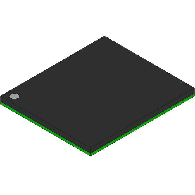
These products are packaged in 165-pin PLASTIC BGA.
Features
• 1.8 ± 0.1 V power supply
• 165-pin PLASTIC BGA (15 x 17)
• HSTL interface
• DLL/PLL circuitry for wide output data valid window and future frequency scaling
• Pipelined double data rate operation
• Common data input/output bus
• Two-tick burst for low DDR transaction size
• Two input clocks (K and K#) for precise DDR timing at clock rising edges only
• Two Echo clocks (CQ and CQ#)
• Data Valid pin (QVLD) supported
• Read latency : 2.0 & 2.5 clock cycles (Not selectable by user)
• Internally self-timed write control
• Clock-stop capability. Normal operation is restored in 20 μs after clock is resumed.
• User programmable impedance output (35 to 70 Ω)
• Fast clock cycle time : 2.5 ns (400 MHz) for 2.0 clock cycles read latency,
2.0 ns (500 MHz) for 2.5 clock cycles read latency
• Simple control logic for easy depth expansion
• JTAG 1149.1 compatible test access port
• On-Die Termination (ODT) for better signal quality (Selectable ON/OFF by user)
The information in this document is subject to change without notice. Before using this document, please
confirm that this is the latest version.
Not all products and/or types are available in every country. Please check with an NEC Electronics
sales representative for availability and additional information.
Document No. M19960EJ2V0DS00 (2nd edition)
Date Published March 2010
Printed in Japan
2009, 2010
�μPD44646092A-A, 44646182A-A, 44646362A-A, 44646093A-A, 44646183A-A, 44646363A-A
Ordering Information
2.0 Clock Cycles Read Latency
Cycle
Clock
Organization
Core
Supply
I/O
Time
Frequency
(word x bit)
Voltage
Interface
ns
MHz
μPD44646092AF5-E25-FQ1-A Note
2.5
400
μPD44646092AF5-E30-FQ1-A
3.0
333
Part number
μPD44646092AF5-E33-FQ1-A
3.3
300
μPD44646182AF5-E25-FQ1-A Note
2.5
400
μPD44646182AF5-E30-FQ1-A
3.0
333
3.3
300
μPD44646182AF5-E33-FQ1-A
μPD44646362AF5-E25-FQ1-A
Note
2.5
400
μPD44646362AF5-E30-FQ1-A
3.0
333
μPD44646362AF5-E33-FQ1-A
3.3
300
Package
V
8M x 9
1.8 ± 0.1
HSTL
165-pin PLASTIC
BGA (15 x 17)
Lead-free
4M x 18
2M x 36
Note Please contact our sales.
2.5 Clock Cycles Read Latency
Part number
Cycle
Clock
Organization
Core Supply
I/O
Time
Frequency
(word x bit)
Voltage
Interface
8M x 9
1.8 ± 0.1
Package
ns
MHz
μPD44646093AF5-E20-FQ1-A Note
2.0
500
μPD44646093AF5-E22-FQ1-A
2.2
450
BGA (15 x 17)
μPD44646093AF5-E25-FQ1-A
2.5
400
Lead-free
μPD44646093AF5-E30-FQ1-A
3.0
333
μPD44646183AF5-E20-FQ1-A Note
2.0
500
μPD44646183AF5-E22-FQ1-A
2.2
450
μPD44646183AF5-E25-FQ1-A
2.5
400
μPD44646183AF5-E30-FQ1-A
3.0
333
μPD44646363AF5-E20-FQ1-A Note
2.0
500
μPD44646363AF5-E22-FQ1-A
2.2
450
μPD44646363AF5-E25-FQ1-A
2.5
400
μPD44646363AF5-E30-FQ1-A
3.0
333
V
4M x 18
2M x 36
Note Please contact our sales.
2
Data Sheet M19960EJ2V0DS
HSTL
165-pin PLASTIC
�μPD44646092A-A, 44646182A-A, 44646362A-A, 44646093A-A, 44646183A-A, 44646363A-A
Feature Differences between DDR II and DDR II+
Features
Frequency (DLL/PLL ON)
Organization
DDR II
DDR II+
200 MHz to 333 MHz
300 MHz to 500 MHz
x9 / x18 / x36
x9 / x18 / x36
Note
1.8 ± 0.1 V
1.8 ± 0.1 V
1.8 ± 0.1 V or 1.5 ± 0.1 V
1.8 ± 0.1 V or 1.5 ± 0.1 V
Read Latency
1.5 clock cycles
2.0 & 2.5 clock cycles
1
Write Latency
1.0 clock cycle
1.0 clock cycle
2
Single Ended (K, K#)
Single Ended (K, K#)
Yes
No
1 Pair
1 Pair
VDD
VDDQ
Input Clocks (K, K#)
Output Clocks (C, C#)
Echo Clock Number (CQ, CQ#)
Package
3
165-pin PLASTIC BGA (15 x 17)
165-pin PLASTIC BGA (15 x 17)
Fixed Burst Address for DDR CIO;
A0 for burst 2
Yes
No
4
QVLD
No
Yes
5
ODT
No
Yes
6
Notes 1. DDR II+ read latency is not user selectable. Offered as two different devices. 2.5 clock cycle is consortium
standard, and 2.0 clock cycle is vendor option.
2. DDR II+ write latency is 1.0 clock cycle regardless of read latency.
3. Echo Clocks are single-ended outputs.
4. Linear burst is not supported at DDR II + CIO.
5. Edge aligned with Echo Clocks.
6. ODT ON/OFF is user selectable.
Data Sheet M19960EJ2V0DS
3
�μPD44646092A-A, 44646182A-A, 44646362A-A, 44646093A-A, 44646183A-A, 44646363A-A
Pin Configurations
165-pin PLASTIC BGA (15 x 17)
(Top View)
[μPD44646092A-A], [μPD44646093A-A]
8M x 9
1
2
3
4
5
6
7
8
9
10
11
A
CQ#
A
A
R, W#
NC
K#
NC/144M
LD#
A
A
CQ
B
NC
NC
NC
A
NC/288M
K
BW0#
A
NC
NC
DQ4
C
NC
NC
NC
VSS
A
A
A
VSS
NC
NC
NC
D
NC
NC
NC
VSS
VSS
VSS
VSS
VSS
NC
NC
NC
E
NC
NC
DQ5
VDDQ
VSS
VSS
VSS
VDDQ
NC
NC
DQ3
F
NC
NC
NC
VDDQ
VDD
VSS
VDD
VDDQ
NC
NC
NC
G
NC
NC
DQ6
VDDQ
VDD
VSS
VDD
VDDQ
NC
NC
NC
H
DLL#
VREF
VDDQ
VDDQ
VDD
VSS
VDD
VDDQ
VDDQ
VREF
ZQ
J
NC
NC
NC
VDDQ
VDD
VSS
VDD
VDDQ
NC
DQ2
NC
K
NC
NC
NC
VDDQ
VDD
VSS
VDD
VDDQ
NC
NC
NC
L
NC
DQ7
NC
VDDQ
VSS
VSS
VSS
VDDQ
NC
NC
DQ1
M
NC
NC
NC
VSS
VSS
VSS
VSS
VSS
NC
NC
NC
N
NC
NC
NC
VSS
A
A
A
VSS
NC
NC
NC
P
NC
NC
DQ8
A
A
QVLD
A
A
NC
NC
DQ0
R
TDO
TCK
A
A
A
ODT
A
A
A
TMS
TDI
A
: Address inputs
TMS
: IEEE 1149.1 Test input
DQ0 to DQ8
: Data inputs / outputs
TDI
: IEEE 1149.1 Test input
LD#
: Synchronous load
TCK
: IEEE 1149.1 Clock input
R, W#
: Read Write input
TDO
: IEEE 1149.1 Test output
BW0#
: Byte Write data select
VREF
: HSTL input reference input
K, K#
: Input clock
VDD
: Power Supply
CQ, CQ#
: Echo clock
VDDQ
: Power Supply
ZQ
: Output impedance matching
VSS
: Ground
DLL#
: DLL/PLL disable
NC
: No connection
QVLD
: Q Valid output
NC/xxM
: Expansion address for xxMb
ODT
: ODT Control Input
Remarks 1. ×××# indicates active LOW signal.
2. Refer to Package Drawing for the index mark.
3. 7A and 5B are expansion addresses: 7A for 144Mb
: 7A and 5B for 288Mb
4
Data Sheet M19960EJ2V0DS
�μPD44646092A-A, 44646182A-A, 44646362A-A, 44646093A-A, 44646183A-A, 44646363A-A
165-pin PLASTIC BGA (15 x 17)
(Top View)
[μPD44646182A-A], [μPD44646183A-A]
4M x 18
1
2
3
4
5
6
7
8
9
10
11
A
CQ#
A
A
R, W#
BW1#
K#
NC/144M
LD#
A
A
CQ
B
NC
DQ9
NC
A
NC/288M
K
BW0#
A
NC
NC
DQ8
C
NC
NC
NC
VSS
A
NC
A
VSS
NC
DQ7
NC
D
NC
NC
DQ10
VSS
VSS
VSS
VSS
VSS
NC
NC
NC
E
NC
NC
DQ11
VDDQ
VSS
VSS
VSS
VDDQ
NC
NC
DQ6
F
NC
DQ12
NC
VDDQ
VDD
VSS
VDD
VDDQ
NC
NC
DQ5
G
NC
NC
DQ13
VDDQ
VDD
VSS
VDD
VDDQ
NC
NC
NC
H
DLL#
VREF
VDDQ
VDDQ
VDD
VSS
VDD
VDDQ
VDDQ
VREF
ZQ
J
NC
NC
NC
VDDQ
VDD
VSS
VDD
VDDQ
NC
DQ4
NC
K
NC
NC
DQ14
VDDQ
VDD
VSS
VDD
VDDQ
NC
NC
DQ3
L
NC
DQ15
NC
VDDQ
VSS
VSS
VSS
VDDQ
NC
NC
DQ2
M
NC
NC
NC
VSS
VSS
VSS
VSS
VSS
NC
DQ1
NC
N
NC
NC
DQ16
VSS
A
A
A
VSS
NC
NC
NC
P
NC
NC
DQ17
A
A
QVLD
A
A
NC
NC
DQ0
R
TDO
TCK
A
A
A
ODT
A
A
A
TMS
TDI
A
: Address inputs
TMS
: IEEE 1149.1 Test input
DQ0 to DQ17
: Data inputs / outputs
TDI
: IEEE 1149.1 Test input
LD#
: Synchronous load
TCK
: IEEE 1149.1 Clock input
R, W#
: Read Write input
TDO
: IEEE 1149.1 Test output
BW0#, BW1#
: Byte Write data select
VREF
: HSTL input reference input
K, K#
: Input clock
VDD
: Power Supply
CQ, CQ#
: Echo clock
VDDQ
: Power Supply
ZQ
: Output impedance matching
VSS
: Ground
DLL#
: DLL/PLL disable
NC
: No connection
QVLD
: Q Valid output
NC/xxM
: Expansion address for xxMb
ODT
: ODT Control Input
Remarks 1. ×××# indicates active LOW signal.
2. Refer to Package Drawing for the index mark.
3. 7A and 5B are expansion addresses: 7A for 144Mb
: 7A and 5B for 288Mb
Data Sheet M19960EJ2V0DS
5
�μPD44646092A-A, 44646182A-A, 44646362A-A, 44646093A-A, 44646183A-A, 44646363A-A
165-pin PLASTIC BGA (15 x 17)
(Top View)
[μPD44646362A-A], [μPD44646363A-A]
2M x 36
1
2
3
4
5
6
7
8
9
10
11
A
CQ#
NC/144M
A
R, W#
BW2#
K#
BW1#
LD#
A
A
CQ
B
NC
DQ27
DQ18
A
BW3#
K
BW0#
A
NC
NC
DQ8
C
NC
NC
DQ28
VSS
A
NC
A
VSS
NC
DQ17
DQ7
D
NC
DQ29
DQ19
VSS
VSS
VSS
VSS
VSS
NC
NC
DQ16
E
NC
NC
DQ20
VDDQ
VSS
VSS
VSS
VDDQ
NC
DQ15
DQ6
F
NC
DQ30
DQ21
VDDQ
VDD
VSS
VDD
VDDQ
NC
NC
DQ5
G
NC
DQ31
DQ22
VDDQ
VDD
VSS
VDD
VDDQ
NC
NC
DQ14
H
DLL#
VREF
VDDQ
VDDQ
VDD
VSS
VDD
VDDQ
VDDQ
VREF
ZQ
J
NC
NC
DQ32
VDDQ
VDD
VSS
VDD
VDDQ
NC
DQ13
DQ4
K
NC
NC
DQ23
VDDQ
VDD
VSS
VDD
VDDQ
NC
DQ12
DQ3
L
NC
DQ33
DQ24
VDDQ
VSS
VSS
VSS
VDDQ
NC
NC
DQ2
M
NC
NC
DQ34
VSS
VSS
VSS
VSS
VSS
NC
DQ11
DQ1
N
NC
DQ35
DQ25
VSS
A
A
A
VSS
NC
NC
DQ10
P
NC
NC
DQ26
A
A
QVLD
A
A
NC
DQ9
DQ0
R
TDO
TCK
A
A
A
ODT
A
A
A
TMS
TDI
A
: Address inputs
TMS
: IEEE 1149.1 Test input
DQ0 to DQ35
: Data inputs / outputs
TDI
: IEEE 1149.1 Test input
LD#
: Synchronous load
TCK
: IEEE 1149.1 Clock input
R, W#
: Read Write input
TDO
: IEEE 1149.1 Test output
BW0# to BW3#
: Byte Write data select
VREF
: HSTL input reference input
K, K#
: Input clock
VDD
: Power Supply
CQ, CQ#
: Echo clock
VDDQ
: Power Supply
ZQ
: Output impedance matching
VSS
: Ground
DLL#
: DLL/PLL disable
NC
: No connection
QVLD
: Q Valid output
NC/xxM
: Expansion address for xxMb
ODT
: ODT Control Input
Remarks 1. ×××# indicates active LOW signal.
2. Refer to Package Drawing for the index mark.
3. 2A is expansion address for 144Mb.
6
Data Sheet M19960EJ2V0DS
�μPD44646092A-A, 44646182A-A, 44646362A-A, 44646093A-A, 44646183A-A, 44646363A-A
Pin Identification
Symbol
Type
A
Input
DQ0 to DQxx
Input/Output
LD#
Input
R, W#
Input
BWx#
Input
K, K#
Input
CQ, CQ#
Output
ZQ
Input
DLL#
Input
QVLD
Output
ODT
Input
TMS
TDI
TCK
Input
TDO
Output
VREF
–
VDD
Supply
VDDQ
Supply
VSS
NC
Supply
–
Input
Description
Synchronous Address Inputs: These inputs are registered and must meet the setup and hold
times around the rising edge of K. All transactions operate on a burst of two words (one clock
period of bus activity). These inputs are ignored when device is deselected, i.e., NOP (LD# =
HIGH).
Synchronous Data IOs: Input data must meet setup and hold times around the rising edges of K
and K#. Output data is synchronized to the respective K and K#.
x9 device uses DQ0 to DQ8.
x18 device uses DQ0 to DQ17.
x36 device uses DQ0 to DQ35.
Synchronous Load: This input is brought LOW when a bus cycle sequence is to be defined.
This definition includes address and read/write direction. All transactions operate on a burst of 2
data (one clock period of bus activity).
Synchronous Read/Write Input: When LD# is LOW, this input designates the access type
(READ when R, W# is HIGH, WRITE when R, W# is LOW) for the loaded address. R, W# must
meet the setup and hold times around the rising edge of K.
Synchronous Byte Writes: When LOW these inputs cause their respective byte to be registered
and written during WRITE cycles. These signals must meet setup and hold times around the
rising edges of K and K# for each of the two rising edges comprising the WRITE cycle. See Pin
Configurations for signal to data relationships.
x9 device uses BW0#.
x18 device uses BW0#, BW1#.
x36 device uses BW0# to BW3#.
See Byte Write Operation for relation between BWx# and DQxx.
Input Clock: This input clock pair registers address and control inputs on the rising edge of K,
and registers data on the rising edge of K and the rising edge of K#. K# is ideally 180 degrees
out of phase with K. All synchronous inputs must meet setup and hold times around the clock
rising edges.
Synchronous Echo Clock Outputs. The rising edges of these outputs are tightly matched to the
synchronous data outputs and can be used as a data valid indication. These signals run freely
and do not stop when DQ tristates. If K and K# are stopped in the single clock mode, CQ and
CQ# will also stop.
Output Impedance Matching Input: This input is used to tune the device outputs to the system
data bus impedance. DQ, CQ, CQ# and QVLD output impedance are set to 0.2 x RQ, where
RQ is a resistor from this bump to ground. The output impedance can be minimized by directly
connect ZQ to VDDQ. This pin cannot be connected directly to GND or left unconnected. The
output impedance is adjusted every 20 μs upon power-up to account for drifts in supply voltage
and temperature. After replacement for a resistor, the new output impedance is reset by
implementing power-on sequence.
DLL/PLL Disable: When DLL# is LOW, the operation can be performed at a clock frequency
slower than TKHKH (MAX.) without the DLL/PLL circuit being used. The AC/DC characteristics
cannot be guaranteed. For normal operation, DLL# must be HIGH and it can be connected to
VDDQ through a 10 kΩ or less resistor.
Q valid Output: The Q Valid indicates valid output data. QVLD is edge aligned with CQ and
CQ#.
ODT Control Input: When the ODT control pin is HIGH, the ODT function is turned on at DQxx
and BWx# pins. The ODT resistors are set to 0.6 x RQ, where RQ is a resistor from ZQ pin
bump to ground. When the ODT Control pin is LOW or No Connect, the ODT function is turned
off. The ODT ON/OFF is set at power-on sequence. The ODT can not change the state after
power-on. To enable ODT function, ODT pin must be HIGH and it can be connected to VDDQ
through a 10 kΩ or less resistor.
IEEE 1149.1 Test Inputs: 1.8 V I/O level. These balls may be left Not Connected if the JTAG
function is not used in the circuit.
IEEE 1149.1 Clock Input: 1.8 V I/O level. This pin must be tied to VSS if the JTAG function is
not used in the circuit.
IEEE 1149.1 Test Output: 1.8 V I/O level.
When providing any external voltage to TDO signal, it is recommended to pull up to VDD.
HSTL Input Reference Voltage: Nominally VDDQ/2. Provides a reference voltage for the input
buffers.
Power Supply: 1.8 V nominal. See Recommended DC Operating Conditions and DC
Characteristics for range.
Power Supply: Isolated Output Buffer Supply. Nominally 1.5 V. 1.8 V is also permissible. See
Recommended DC Operating Conditions and DC Characteristics for range.
Power Supply: Ground
No Connect: These signals are not connected internally.
Data Sheet M19960EJ2V0DS
7
�μPD44646092A-A, 44646182A-A, 44646362A-A, 44646093A-A, 44646183A-A, 44646363A-A
Block Diagram
x9/x18/x36
Write Register
A
Address
Register
Write Driver
x9/x18/x36
DQx
Add.
Dec.
K#
K
CLK
Gen.
DLL#
R, W#
BWx#
LD#
8
Output
Buffer
Memory Array
CQ
QVLD
Sense AMPs
MUX
Control
Logic
CQ#
x18/x36/x72
x18/x36/x72
Output Register
Data Sheet M19960EJ2V0DS
�μPD44646092A-A, 44646182A-A, 44646362A-A, 44646093A-A, 44646183A-A, 44646363A-A
Power-On Sequence in DDR II+ SRAM
DDR II+ SRAMs must be powered up and initialized in a predefined manner to prevent undefined operations.
The following timing charts show the recommended power-on sequence.
The following power-up supply voltage application is recommended: VSS, VDD, VDDQ, VREF, then VIN. VDD and VDDQ
can be applied simultaneously, as long as VDDQ does not exceed VDD by more than 0.5 V during power-up. The
following power-down supply voltage removal sequence is recommended: VIN, VREF, VDDQ, VDD, VSS. VDD and VDDQ
can be removed simultaneously, as long as VDDQ does not exceed VDD by more than 0.5 V during power-down.
Power-On Sequence
Apply power and tie DLL# to HIGH.
- Apply VDD before VDDQ.
- Apply VDDQ before VREF or at the same time as VREF.
Select ODT ON/OFF.
Provide stable clock for more than 20 μs to lock the DLL/PLL.
DLL/PLL Constraints
The DLL/PLL uses K clock as its synchronizing input and the input should have low phase jitter which is specified
as TKC var. The DLL/PLL can cover 190 MHz as the lowest frequency. If the input clock is unstable and the
DLL/PLL is enabled, then the DLL/PLL may lock onto an undesired clock frequency.
ODT initialization
The ODT ON/OFF is set at power-on sequence. When the ODT Control pin is HIGH before applying stable clock,
the ODT function is turn on. When the ODT Control pin is LOW or No Connect, the ODT function is off. The ODT
can not change the state after power-on.
Power-On Waveforms
VDD/VDDQ
VDD/VDDQ Stable (< ±0.1 V DC per 50 ns)
DLL#
Fix HIGH (or tied to VDDQ)
ODT
Fix HIGH or LOW (or No Connect)
Clock
Unstable Clock
20 μs or more
Stable Clock
Data Sheet M19960EJ2V0DS
Normal Operation
Start
9
�μPD44646092A-A, 44646182A-A, 44646362A-A, 44646093A-A, 44646183A-A, 44646363A-A
On-Die Termination (ODT)
On-Die Termination (ODT) is enabled by setting ODT control pin to HIGH at power-on sequence. The ODT resistors
(RTT) are set to 0.6 x RQ, where RQ is a resistor from ZQ pin bump to ground. With ODT on, all the DQs and BW#s are
terminated to VDDQ and VSS with a resistance RTT x 2. The command, address, and clock signals are not terminated.
Figure below shows the equivalent circuit of a DQxx and BWx# receiver with ODT. ODT of DQs are dynamically
switched off before a half cycle when READ commands starts and are designed to be off prior to the product driving the
bus. ODT of BW#s are always on. Similarly, ODTs are designed to switch on after a half cycle when the product has
issued the last piece of data.
When the ODT control pin is LOW or No Connect at power-on sequence, the ODT function is always off.
When the ODT be changed the state after power-on, the AC/DC characteristics cannot be guaranteed.
On-Die Termination DC Parameters
Description
Symbol
MIN.
TYP.
MAX.
Units
On-Die termination
RTT
105
150
210
Ω
External matching resistor
RQ
175
250
350
Ω
The allowable range of RQ to guarantee impedance matching a tolerance of ± 20 % is between 175 Ω
and 350 Ω.
Remark
On- Die Termination-Equivalent Circuit
VDDQ
SW
RTT x 2
Receiver
DQxx, BWx#
RTT x 2
SW
VSS
QDRTM Consortium specification for ODT is defined when 6R is HIGH and vendor specification when 6R is LOW or
Floating. NEC specification is "Disabled" with 6R LOW or Floating as follows.
ODT-option clarification
6R input
ODT function
Consortium specification
NEC specification
Consortium specification
NEC specification
HIGH
Active
Active
RTT = 0.6 x RQ
LOW
Vendor specification
Disabled
Vendor specification
–
Floating
Vendor specification
Disabled
Vendor specification
–
Note
10
Termination value
In case of nominal value (RQ = 250 Ω), RTT = 150 Ω.
Data Sheet M19960EJ2V0DS
RTT = 0.6 x RQ
�μPD44646092A-A, 44646182A-A, 44646362A-A, 44646093A-A, 44646183A-A, 44646363A-A
Truth Table
2.0 Clock Cycles Read Latency
[μPD44646092A-A], [μPD44646182A-A], [μPD44646362A-A]
Operation
WRITE cycle
CLK
LD#
R,W#
L→H
L
L
DQ
Data in
Load address, input write data on
Input data
DA(A+0)
DA(A+1)
consecutive K and K# rising edge
Input clock
K(t+1) ↑
K#(t+1) ↑
Load address, read data on
Output data
QA(A+0)
QA(A+1)
consecutive K and K# rising edge
Output clock
K(t+2) ↑
K#(t+2) ↑
L→H
READ cycle
NOP (No operation)
Clock stop
L
H
Data out
L→H
H
X
DQ = High-Z
Stopped
X
X
Previous state
2.5 Clock Cycles Read Latency
[μPD44646093A-A], [μPD44646183A-A], [μPD44646363A-A]
Operation
WRITE cycle
CLK
LD#
R,W#
L→H
L
L
DQ
Data in
Load address, input write data on
Input data
DA(A+0)
DA(A+1)
consecutive K and K# rising edge
Input clock
K(t+1) ↑
K#(t+1) ↑
Load address, read data on
Output data
QA(A+0)
QA(A+1)
consecutive K and K# rising edge
Output clock
K#(t+2) ↑
K(t+3) ↑
L→H
READ cycle
NOP (No operation)
Clock stop
Remarks
L
H
Data out
L→H
H
X
DQ = High-Z
Stopped
X
X
Previous state
Remarks listed below are for both products with 2.0 and 2.5 Clock Cycles Read Latency.
1. H : HIGH, L : LOW, × : don’t care, ↑ : rising edge.
2. Data inputs are registered at K and K# rising edges. Data outputs are delivered at K and K# rising edges.
3. All control inputs in the truth table must meet setup/hold times around the rising edge (LOW to HIGH) of
K. All control inputs are registered during the rising edge of K.
4. This device contains circuitry that ensure the outputs to be in high impedance during power-up.
5. Refer to state diagram and timing diagrams for clarification.
6. A+0 refers to the address input during a WRITE or READ cycle.
A+1 refers to the next internal burst address in accordance with the burst sequence.
7. It is recommended that K = K# when clock is stopped. This is not essential but permits most rapid restart
by overcoming transmission line charging symmetrically.
Data Sheet M19960EJ2V0DS
11
�μPD44646092A-A, 44646182A-A, 44646362A-A, 44646093A-A, 44646183A-A, 44646363A-A
Byte Write Operation
[μPD44646092A-A], [μPD44646093A-A]
Operation
Write DQ0 to DQ8
Write nothing
K
K#
BW0#
L→H
–
0
–
L→H
0
L→H
–
1
–
L→H
1
Remarks 1. H : HIGH, L : LOW, → : rising edge.
2. Assumes a WRITE cycle was initiated. BW0# can be altered for any portion of the BURST WRITE
operation provided that the setup and hold requirements are satisfied.
[μPD44646182A-A], [μPD44646183A-A]
Operation
K
K#
BW0#
BW1#
L→H
–
0
0
–
L→H
0
0
Write DQ0 to DQ8
L→H
–
0
1
–
L→H
0
1
Write DQ9 to DQ17
L→H
–
1
0
–
L→H
1
0
Write nothing
L→H
–
1
1
–
L→H
1
1
Write DQ0 to DQ17
Remarks 1. H : HIGH, L : LOW, → : rising edge.
2. Assumes a WRITE cycle was initiated. BW0# and BW1# can be altered for any portion of the BURST
WRITE operation provided that the setup and hold requirements are satisfied.
[μPD44646362A-A], [μPD44646363A-A]
Operation
K#
BW0#
BW1#
BW2#
BW3#
L→H
–
0
0
0
0
–
L→H
0
0
0
0
L→H
–
0
1
1
1
–
L→H
0
1
1
1
Write DQ9 to DQ17
L→H
–
1
0
1
1
–
L→H
1
0
1
1
Write DQ18 to DQ26
L→H
–
1
1
0
1
–
L→H
1
1
0
1
Write DQ27 to DQ35
L→H
–
1
1
1
0
–
L→H
1
1
1
0
Write nothing
L→H
–
1
1
1
1
–
L→H
1
1
1
1
Write DQ0 to DQ35
Write DQ0 to DQ8
K
Remarks 1. H : HIGH, L : LOW, → : rising edge.
2. Assumes a WRITE cycle was initiated. BW0# to BW3# can be altered for any portion of the BURST
WRITE operation provided that the setup and hold requirements are satisfied.
12
Data Sheet M19960EJ2V0DS
�μPD44646092A-A, 44646182A-A, 44646362A-A, 44646093A-A, 44646183A-A, 44646363A-A
Bus Cycle State Diagram
LOAD NEW
ADDRESS
Count = 0
Load, Count = 2
Load, Count = 2
Write
Read
READ DOUBLE
Count = Count + 2
WRITE DOUBLE
Count = Count + 2
NOP,
Count = 2
NOP,
Count = 2
Load
NOP
NOP
Power UP
Supply voltage provided
Remarks 1. Bus cycle is terminated after burst count = 2.
2. State machine control timing sequence is controlled by K.
Data Sheet M19960EJ2V0DS
13
�μPD44646092A-A, 44646182A-A, 44646362A-A, 44646093A-A, 44646183A-A, 44646363A-A
Electrical Specifications
Absolute Maximum Ratings
Parameter
Rating
Unit
VDD
–0.5 to +2.5
V
VDDQ
–0.5 to VDD
V
Input voltage
VIN
–0.5 to VDD + 0.5 (2.5 V MAX.)
V
Input / Output voltage
VI/O
–0.5 to VDDQ + 0.5 (2.5 V MAX.)
V
Operating ambient temperature
TA
0 to 70
°C
Storage temperature
Tstg
–55 to +125
°C
Supply voltage
Output supply voltage
Symbol
Conditions
Caution Exposing the device to stress above those listed in Absolute Maximum Ratings could cause
permanent damage. The device is not meant to be operated under conditions outside the limits
described in the operational section of this specification. Exposure to Absolute Maximum Rating
conditions for extended periods may affect device reliability.
Recommended DC Operating Conditions (TA = 0 to 70°C)
Parameter
MIN.
TYP.
MAX.
Unit
VDD
1.7
1.8
1.9
V
Output supply voltage
VDDQ
1.4
VDD
V
1
Input HIGH voltage
VIH (DC)
VREF + 0.1
VDDQ + 0.3
V
1, 2
Input LOW voltage
VIL (DC)
–0.3
VREF – 0.1
V
1, 2
Clock input voltage
VIN
–0.3
VDDQ + 0.3
V
1, 2
Reference voltage
VREF
0.68
0.95
V
Supply voltage
Symbol
Conditions
Note
Notes 1. During normal operation, VDDQ must not exceed VDD.
2. Power-up: VIH ≤ VDDQ + 0.3 V and VDD ≤ 1.7 V and VDDQ ≤ 1.4 V for t ≤ 200 ms
Recommended AC Operating Conditions (TA = 0 to 70°C)
Parameter
Symbol
Input HIGH voltage
VIH (AC)
Input LOW voltage
VIL (AC)
Conditions
MIN.
MAX.
VREF + 0.2
VREF – 0.2
Unit
Note
V
1
V
1
Note 1. Overshoot: VIH (AC) ≤ VDD + 0.7 V (2.5 V MAX.) for t ≤ TKHKH/2
Undershoot: VIL (AC) ≥ – 0.5 V for t ≤ TKHKH/2
Control input signals may not have pulse widths less than TKHKL (MIN.) or operate at cycle rates less than
TKHKH (MIN.).
14
Data Sheet M19960EJ2V0DS
�μPD44646092A-A, 44646182A-A, 44646362A-A, 44646093A-A, 44646183A-A, 44646363A-A
DC Characteristics (TA = 0 to 70°C, VDD = 1.8 ± 0.1 V)
Parameter
Symbol
Test condition
MIN.
MAX.
x9
Input leakage current
ILI
I/O leakage current
ILO
Operating supply current
IDD
(Read cycle / Write cycle)
VIN ≤ VIL or VIN ≥ VIH
ISB1
(NOP)
Output HIGH voltage
VOH(Low)
VOH
Output LOW voltage
VOL(Low)
VOL
x36
+2
μA
4, 5
–2
+2
μA
4
-E20
Note1
690
740
850
II/O = 0 mA
-E22
Note1
650
695
790
Cycle = MAX.
-E25
610
650
730
-E30
530
590
670
490
560
640
VIN ≤ VIL or VIN ≥ VIH
-E20
Note1
II/O = 0 mA
-E22
Note1
Cycle = MAX.
-E25
410
430
480
Inputs static
-E30
380
400
450
-E33
370
390
430
|IOH| ≤ 0.1 mA
Note2
Note3
440
470
530
430
450
505
VDDQ – 0.2
VDDQ
VDDQ/2–0.12
VDDQ/2+0.12
VSS
0.2
VDDQ/2–0.12
VDDQ/2+0.12
IOL ≤ 0.1 mA
Note
–2
-E33
Standby supply current
x18
Unit
mA
mA
V
6, 7
6, 7
V
6, 7
6, 7
Notes 1. -E20 and -E22 are valid for 2.5 Clock Cycles Read Latency products.
2. Outputs are impedance-controlled. | IOH | = (VDDQ/2)/(RQ/5) ±15% for values of 175 Ω ≤ RQ ≤ 350 Ω.
3. Outputs are impedance-controlled. IOL = (VDDQ/2)/(RQ/5) ±15% for values of 175 Ω ≤ RQ ≤ 350 Ω.
4. Measured with ODT off.
5. ODT pin is internally tied to VSS, so input leakage current value is ±5 μA.
6. AC load current is higher than the shown DC values.
7. HSTL outputs meet JEDEC HSTL Class I standards.
Capacitance (TA = 25°C, f = 1 MHz)
Parameter
Symbol
Test conditions
MIN.
MAX.
Unit
Input capacitance (Address, Control)
CIN
VIN = 0 V
4
pF
Input / Output capacitance
CI/O
VI/O = 0 V
5
pF
Cclk
Vclk = 0 V
4
pF
(DQ, CQ, CQ#, QVLD)
Clock Input capacitance
Remark These parameters are periodically sampled and not 100% tested.
Data Sheet M19960EJ2V0DS
15
�μPD44646092A-A, 44646182A-A, 44646362A-A, 44646093A-A, 44646183A-A, 44646363A-A
Thermal Characteristics
Parameter
Thermal resistance
Symbol
θ ja
Substrate
4-layer
from junction to ambient air
8-layer
Thermal characterization parameter
Ψ jt
4-layer
from junction to the top center
of the package surface
Thermal resistance
8-layer
θ jc
from junction to case
16
Data Sheet M19960EJ2V0DS
Airflow
TYP.
Unit
0 m/s
19.5
°C/W
1 m/s
12.0
°C/W
0 m/s
18.1
°C/W
1 m/s
11.3
°C/W
0 m/s
0.01
°C/W
1 m/s
0.05
°C/W
0 m/s
0.01
°C/W
1 m/s
0.04
°C/W
2.14
°C/W
�μPD44646092A-A, 44646182A-A, 44646362A-A, 44646093A-A, 44646183A-A, 44646363A-A
AC Characteristics (TA = 0 to 70°C, VDD = 1.8 ± 0.1 V)
AC Test Conditions (VDD = 1.8 ± 0.1 V, VDDQ = 1.4 to VDD)
Input waveform (Rise / Fall time ≤ 0.3 ns)
1.25 V
0.75 V
Test Points
0.75 V
0.25 V
Output waveform
Test Points
VDDQ / 2
VDDQ / 2
Output load condition
Figure 1. External load at test
VDDQ / 2
0.75 V
50 Ω
VREF
ZO = 50 Ω
SRAM
250 Ω
ZQ
Data Sheet M19960EJ2V0DS
17
�μPD44646092A-A, 44646182A-A, 44646362A-A, 44646093A-A, 44646183A-A, 44646363A-A
Read and Write Cycle
Parameter
Symbol
-E20
Note1
(500 MHz)
-E22
Note1
-E25
(450 MHz)
(400 MHz)
-E30
(333 MHz)
-E33
Unit
Note
5.25
ns
2
0.20
ns
3
(300 MHz)
MIN. MAX. MIN. MAX. MIN. MAX. MIN. MAX. MIN. MAX.
Clock
Average Clock cycle time (K, K#)
TKHKH
Clock phase jitter (K, K#)
TKC var
Clock HIGH time (K, K#)
TKHKL
0.4
0.4
0.4
0.4
0.4
TKHKH
Clock LOW time (K, K#)
TKLKH
0.4
0.4
0.4
0.4
0.4
TKHKH
TKHK#H
0.85
0.95
1.06
1.28
1.40
ns
TK#HKH
0.85
0.95
1.06
1.28
1.40
ns
DLL/PLL lock time (K)
TKC lock
20
20
20
20
20
μs
4
K static to DLL/PLL reset
TKC reset
30
30
30
30
30
ns
5
TCQHCQ#H
0.6
0.7
0.81
1.03
1.15
ns
6
TCQ#HCQH
0.6
0.7
0.81
1.03
1.15
ns
6
Clock HIGH to Clock# HIGH
(K → K#)
Clock# HIGH to Clock HIGH
(K# → K)
2.0
5.25
2.2
0.15
5.25
2.5
0.15
5.25
3.0
0.20
5.25
3.3
0.20
Output Times
CQ HIGH to CQ# HIGH
(CQ → CQ#)
CQ# HIGH to CQ HIGH
(CQ# → CQ)
K, K# HIGH to output valid
TKHQV
K, K# HIGH to output hold
TKHQX
K, K# HIGH to echo clock valid
TKHCQV
K, K# HIGH to echo clock hold
TKHCQX
CQ, CQ# HIGH to output valid
TCQHQV
CQ, CQ# HIGH to output hold
TCQHQX
K HIGH to output High-Z
TKHQZ
K HIGH to output Low-Z
TKHQX1
CQ, CQ# HIGH to QVLD valid
0.45
– 0.45
0.45
– 0.45
0.45
– 0.45
0.45
– 0.45
0.15
– 0.15
– 0.45
– 0.15
– 0.45
– 0.20
0.20
0.45
ns
ns
0.20
– 0.20
0.45
– 0.45
ns
ns
0.45
– 0.45
– 0.20
– 0.45
0.45
– 0.45
0.45
0.20
0.45
– 0.45
0.45
– 0.45
0.45
0.15
0.45
– 0.45
0.45
– 0.45
0.45
– 0.45
TCQHQVLD – 0.15 0.15 – 0.15 0.15 – 0.20 0.20 – 0.20 0.20 – 0.20 0.20
ns
7
ns
7
ns
ns
ns
Setup Times
Address valid to K rising edge
Synchronous load input (LD#),
read write input (R, W#) valid to
K rising edge
Data inputs and write data select
inputs (BWx#) valid to
K, K# rising edge
TAVKH
0.33
0.4
0.4
0.4
0.4
ns
8
TIVKH
0.33
0.4
0.4
0.4
0.4
ns
8
TDVKH
0.25
0.28
0.28
0.28
0.28
ns
8
TKHAX
0.33
0.4
0.4
0.4
0.4
ns
8
TKHIX
0.33
0.4
0.4
0.4
0.4
ns
8
TKHDX
0.25
0.28
0.28
0.28
0.28
ns
8
Hold Times
K rising edge to address hold
K rising edge to
synchronous load input (LD#),
read write input (R, W#) hold
K, K# rising edge to data inputs
and write data select inputs
(BWx#) hold
Notes 1. -E20 and –E22 are valid for 2.5 Clock Cycles Read Latency products.
2. When debugging the system or board, these products can operate at a clock frequency slower than TKHKH
(MAX.) without the DLL/PLL circuit being used, if DLL# = LOW. Read latency (RL) is changed to 1.0 clock
cycle regardless of RL = 2.0 and 2.5 clock cycles products in this operation. The AC/DC characteristics
cannot be guaranteed, however.
3. Clock phase jitter is the variance from clock rising edge to the next expected clock rising edge. TKC var
(MAX.) indicates a peak-to-peak value.
18
Data Sheet M19960EJ2V0DS
�μPD44646092A-A, 44646182A-A, 44646362A-A, 44646093A-A, 44646183A-A, 44646363A-A
4. VDD slew rate must be less than 0.1 V DC per 50 ns for DLL/PLL lock retention.
DLL/PLL lock time begins once VDD and input clock are stable.
It is recommended that the device is kept NOP (LD# = HIGH) during these cycles.
5. K input is monitored for this operation. See below for the timing.
K
TKC reset
or
K
TKC reset
6. Guaranteed by design.
7. Echo clock is very tightly controlled to data valid / data hold. By design, there is a ± 0.1 ns variation from
echo clock to data. The data sheet parameters reflect tester guardbands and test setup variations.
8. This is a synchronous device. All addresses, data and control lines must meet the specified setup
and hold times for all latching clock edges.
Remarks 1. This parameter is sampled.
2. Test conditions as specified with the output loading as shown in AC Test Conditions
unless otherwise noted.
3. Control input signals may not be operated with pulse widths less than TKHKL (MIN.).
4. VDDQ is 1.5 V DC.
Data Sheet M19960EJ2V0DS
19
�μPD44646092A-A, 44646182A-A, 44646362A-A, 44646093A-A, 44646183A-A, 44646363A-A
Read and Write Timing
2.0 Clock Cycles Read Latency
[μPD44646092A-A], [μPD44646182A-A], [μPD44646362A-A]
NOP
READ
READ
NOP
(burst of 2) (burst of 2)
1
2
3
NOP
NOP
4
5
6
READ
WRITE
WRITE
(burst of 2) (burst of 2) (burst of 2)
7
8
9
A2
A3
A4
10
11
TKHKH
K
TKHKL TKLKH
TKHK#H
TK#HKH
K#
LD#
TIVKH
TKHIX
R, W#
TAVKH
Address
ODT state
DQ
TKHAX
A0
A1
ODT-ON
ODT-ON
ODT-OFF
ODT state
BW#
ODT-OFF
ODT-ON
TCQHQVLD
TCQHQVLD
QVLD
Read Latency = 2.0 clock cycles
TKHQV
TKHQX
TKHQV
TKHQX
TKHDX
TKHDX
TKHQZ
TDVKH
TDVKH
TKHCQX1
DQ
Q00
Q01
TCQHQX
TKHCQV
Q10
Q11
D20
D21
D30
D31
Q40
Q41
TCQHQX
TCQHQV
TCQHQV
TKHCQX
CQ
TCQHCQ#H TCQ#HCQH
TKHCQV
TKHCQX
CQ#
Remarks 1. Q00 refers to output from address A0.
Q01 refers to output from the next internal burst address following A0, etc.
2. Outputs are disabled (high impedance) 3 clock cycles after the last READ (LD# = LOW, R, W# = HIGH)
is input in the sequences of [READ]-[NOP].
3. The third NOP cycle between Read to Write transition may not be necessary for correct device
operation when Read latency = 2.0 clock cycles. However, it may be required to avoid bus contention.
4. When the ODT control pin is LOW or No Connect, the ODT function is always off.
20
Data Sheet M19960EJ2V0DS
�μPD44646092A-A, 44646182A-A, 44646362A-A, 44646093A-A, 44646183A-A, 44646363A-A
2.5 Clock Cycles Read Latency
[μPD44646093A-A], [μPD44646183A-A], [μPD44646363A-A]
NOP
READ
READ
(burst of 2) (burst of 2)
1
2
3
NOP
NOP
4
5
NOP
6
WRITE
WRITE
READ
(burst of 2) (burst of 2) (burst of 2)
7
8
9
A2
A3
A4
10
11
TKHKH
K
TKHKL TKLKH
TKHK#H
TK#HKH
K#
LD#
TIVKH
TKHIX
R, W#
TAVKH TKHAX
Address
ODT state
DQ
A0
A1
ODT-ON
ODT-ON
ODT-OFF
ODT state
BW#
ODT-OFF
ODT-ON
TCQHQVLD
TCQHQVLD
QVLD
Read Latency = 2.5 clock cycles
TKHQV
TKHQX
TKHQV
TKHDX
TKHDX
TKHQX
TDVKH
TDVKH
TKHQZ
TKHCQX1
DQ
Q00
Q01
TCQHQX
TKHCQV
TCQHQV
Q10
Q11
D20
D21
D30
D31
TCQHQX
TCQHQV
TKHCQX
CQ
TCQHCQ#H TCQ#HCQH
TKHCQV
TKHCQX
CQ#
Remarks 1. Q00 refers to output from address A0.
Q01 refers to output from the next internal burst address following A0, etc.
2. Outputs are disabled (high impedance) 3.5 clock cycles after the last READ (LD# = LOW, R, W# = HIGH)
is input in the sequences of [READ]-[NOP].
3. When the ODT control pin is LOW or No Connect, the ODT function is always off.
Data Sheet M19960EJ2V0DS
21
�μPD44646092A-A, 44646182A-A, 44646362A-A, 44646093A-A, 44646183A-A, 44646363A-A
Application Example
ZQ
CQ#
CQ
QVLD
SRAM#1
DQ
SRAM
Controller
Vt
A
LD#
R, W#
BWx#
R=
250 Ω
...
K/K#
SRAM#4
DQ
A
LD#
R, W#
BWx#
ZQ
CQ#
CQ
QVLD
R=
250 Ω
K/K#
R
Data IO
Address
LD#
R, W#
BW#
QVLD
Vt
...
SRAM#1 CQ/CQ#
R
Vt
SRAM#4 CQ/CQ#
R
Vt
R
Source CLK/CLK#
Return CLK/CLK#
Vt
R
R = 50 Ω Vt = Vref
Remark
AC specifications are defined at the condition of SRAM outputs, CQ, CQ#, QVLD and DQ with termination.
DQs and BW#s have ODT.
22
Data Sheet M19960EJ2V0DS
�μPD44646092A-A, 44646182A-A, 44646362A-A, 44646093A-A, 44646183A-A, 44646363A-A
JTAG Specification
These products support a limited set of JTAG functions as in IEEE standard 1149.1.
Test Access Port (TAP) Pins
Pin name
Pin assignments
Description
TCK
2R
Test Clock Input. All input are captured on the rising edge of TCK and all outputs
propagate from the falling edge of TCK.
TMS
10R
Test Mode Select. This is the command input for the TAP controller state machine.
TDI
11R
Test Data Input. This is the input side of the serial registers placed between TDI and
TDO. The register placed between TDI and TDO is determined by the state of the TAP
controller state machine and the instruction that is currently loaded in the TAP instruction.
TDO
1R
Test Data Output. This is the output side of the serial registers placed between TDI and
TDO. Output changes in response to the falling edge of TCK.
Remark The device does not have TRST (TAP reset). The Test-Logic Reset state is entered while TMS is held HIGH
for five rising edges of TCK. The TAP controller state is also reset on the SRAM POWER-UP.
JTAG DC Characteristics (TA = 0 to 70°C, VDD = 1.8 ± 0.1 V, unless otherwise noted)
Parameter
Symbol
Conditions
MIN.
MAX.
Unit
JTAG Input leakage current
ILI
0 V ≤ VIN ≤ VDD
−5.0
+5.0
μA
JTAG I/O leakage current
ILO
0 V ≤ VIN ≤ VDDQ,
−5.0
+5.0
μA
Outputs disabled
JTAG input HIGH voltage
VIH
1.3
VDD+0.3
V
JTAG input LOW voltage
VIL
−0.3
+0.5
V
JTAG output HIGH voltage
JTAG output LOW voltage
VOH1
| IOHC | = 100 μA
1.6
V
VOH2
| IOHT | = 2 mA
1.4
V
VOL1
IOLC = 100 μA
0.2
V
VOL2
IOLT = 2 mA
0.4
V
Data Sheet M19960EJ2V0DS
23
�μPD44646092A-A, 44646182A-A, 44646362A-A, 44646093A-A, 44646183A-A, 44646363A-A
JTAG AC Test Conditions
Input waveform (Rise / Fall time ≤ 1 ns)
1.8 V
0.9 V
Test Points
0.9 V
0.9 V
Test Points
0.9 V
0V
Output waveform
Output load
Figure 2. External load at test
VTT = 0.9 V
50 Ω
ZO = 50 Ω
TDO
20 pF
24
Data Sheet M19960EJ2V0DS
�μPD44646092A-A, 44646182A-A, 44646362A-A, 44646093A-A, 44646183A-A, 44646363A-A
JTAG AC Characteristics (TA = 0 to 70°C)
Parameter
Symbol
Conditions
MIN.
MAX.
Unit
20
MHz
Clock
Clock cycle time
tTHTH
Clock frequency
fTF
50
ns
Clock HIGH time
tTHTL
20
ns
Clock LOW time
tTLTH
20
ns
TCK LOW to TDO unknown
tTLOX
0
ns
TCK LOW to TDO valid
tTLOV
Output time
10
ns
Setup time
TMS setup time
tMVTH
5
ns
TDI valid to TCK HIGH
tDVTH
5
ns
tCS
5
ns
TMS hold time
tTHMX
5
ns
TCK HIGH to TDI invalid
tTHDX
5
ns
tCH
5
ns
Capture setup time
Hold time
Capture hold time
JTAG Timing Diagram
tTHTH
TCK
tMVTH
tTHTL
tTLTH
TMS
tTHMX
tDVTH
TDI
tTHDX
tTLOX
tTLOV
TDO
Data Sheet M19960EJ2V0DS
25
�μPD44646092A-A, 44646182A-A, 44646362A-A, 44646093A-A, 44646183A-A, 44646363A-A
Scan Register Definition (1)
Register name
Description
Instruction register
The instruction register holds the instructions that are executed by the TAP controller when it is
moved into the run-test/idle or the various data register state. The register can be loaded when it is
placed between the TDI and TDO pins. The instruction register is automatically preloaded with the
IDCODE instruction at power-up whenever the controller is placed in test-logic-reset state.
Bypass register
The bypass register is a single bit register that can be placed between TDI and TDO. It allows serial
test data to be passed through the RAMs TAP to another device in the scan chain with as little delay
as possible.
ID register
The ID Register is a 32 bit register that is loaded with a device and vendor specific 32 bit code when
the controller is put in capture-DR state with the IDCODE command loaded in the instruction register.
The register is then placed between the TDI and TDO pins when the controller is moved into shift-DR
state.
Boundary register
The boundary register, under the control of the TAP controller, is loaded with the contents of the
RAMs I/O ring when the controller is in capture-DR state and then is placed between the TDI and
TDO pins when the controller is moved to shift-DR state. Several TAP instructions can be used to
activate the boundary register.
The Scan Exit Order tables describe which device bump connects to each boundary register
location. The first column defines the bit’s position in the boundary register. The second column is
the name of the input or I/O at the bump and the third column is the bump number.
Scan Register Definition (2)
Register name
Bit size
Unit
Instruction register
3
bit
Bypass register
1
bit
ID register
32
bit
Boundary register
109
bit
ID Register Definition
2.0 Clock Cycles Read Latency
Part number
Organization
ID [31:28] vendor revision no.
ID [27:12] part no.
ID [11:1] vendor ID no. ID [0] fix bit
μPD44646092A-A
8M x 9
XXXX
0000 0000 1000 1100
00000010000
1
μPD44646182A-A
4M x 18
XXXX
0000 0000 1000 1101
00000010000
1
μPD44646362A-A
2M x 36
XXXX
0000 0000 1000 1110
00000010000
1
2.5 Clock Cycles Read Latency
Part number
Organization
ID [31:28] vendor revision no.
ID [27:12] part no.
μPD44646093A-A
8M x 9
XXXX
0000 0000 1001 1000
00000010000
1
μPD44646183A-A
4M x 18
XXXX
0000 0000 1001 1001
00000010000
1
μPD44646363A-A
2M x 36
XXXX
0000 0000 1001 1010
00000010000
1
26
Data Sheet M19960EJ2V0DS
ID [11:1] vendor ID no. ID [0] fix bit
�μPD44646092A-A, 44646182A-A, 44646362A-A, 44646093A-A, 44646183A-A, 44646363A-A
SCAN Exit Order
Bit
no.
Signal name
x9
x18
x36
Bump
Bit
ID
no.
6R
37
1
ODT
2
QVLD
6P
38
3
A
6N
39
4
A
5
A
6
A
7
A
8
A
9
A
10
11
NC
NC
12
13
NC
15
NC
NC
17
NC
18
19
NC
NC
20
NC
21
NC
22
NC
23
NC
3E
10C
75
DQ7 DQ17
NC DQ16
11D
NC
NC DQ29
2D
76
NC
2E
1E
42
9D
78
NC DQ12 DQ30
2F
8R
43
DQ4 DQ8 DQ8
11B
79
NC
44
NC
NC
DQ7
11C
NC DQ21
3F
80
NC
1G
1F
3G
45
NC
9B
81
NC
11P
46
NC
10B
82
DQ6 DQ13 DQ22
10P
47
CQ
11A
83
48
A
10A
84
DLL#
1H
49
A
85
NC
1J
50
A
8B
86
NC
2J
51
A
7C
87
NC DQ14 DQ23
3K
52
NC
6C
88
NC
NC DQ32
3J
89
NC
2K
1K
2L
9M
9N
11L
11M
9L
10L
A
9A
NC
LD#
53
8A
NC
NC DQ31
7A
90
NC
55
BW0#
7B
91
DQ7 DQ15 DQ33
56
K
6B
92
57
K#
54
NC
NC BW1#
6A
NC
2G
NC DQ24
3L
93
NC
1M
1L
NC BW3#
5B
94
NC DQ12
10K
59
NC BW1# BW2#
5A
95
NC DQ16 DQ25
3N
9J
60
4A
96
NC
NC DQ34
3M
97
NC
1N
2M
3P
NC
28
29
NC
30
NC
NC
DQ5 DQ11 DQ20
NC
ZQ
32
74
7R
9P
9K
DQ2 DQ4 DQ13
NC
9E
58
25
31
2C
NC
11K
NC
NC
NC
ID
DQ3 DQ3
24
27
73
x36
NC
NC
26
10D
x18
77
10N
DQ1
NC
x9
9C
9R
DQ1 DQ2 DQ2
no.
x36
Bump
NC
NC DQ10 11N
16
NC
ID
x18
Signal name
41
DQ1 DQ11 10M
NC
NC
Bit
NC
8P
DQ9
40
x9
Bump
NC
7N
DQ0
NC
14
7P
Signal name
DQ4
DQ5 DQ5
R, W#
61
A
5C
10J
62
A
4B
98
NC
11J
63
A
3A
99
DQ8 DQ17 DQ26
11H
64
2A
100
10G
A
65
NC
CQ#
9G
66
NC
11F
67
NC
NC DQ14 11G
A
1A
NC
NC DQ35
2N
101
NC
2P
1P
DQ9 DQ27
2B
102
NC
NC DQ18
3B
103
A
3R
68
NC
1C
104
A
4R
1B
105
A
4P
33
NC
9F
69
NC
34
NC
10F
70
NC DQ10 DQ19
3D
106
A
5P
35
DQ3 DQ6 DQ6
11E
71
NC
NC DQ28
3C
107
A
5N
NC
1D
108
A
5R
109
–
Internal
36
NC
NC DQ15
10E
72
Data Sheet M19960EJ2V0DS
27
�μPD44646092A-A, 44646182A-A, 44646362A-A, 44646093A-A, 44646183A-A, 44646363A-A
JTAG Instructions
Instructions
EXTEST
Description
The EXTEST instruction allows circuitry external to the component package to be tested. Boundaryscan register cells at output pins are used to apply test vectors, while those at input pins capture test
results. Typically, the first test vector to be applied using the EXTEST instruction will be shifted into the
boundary scan register using the PRELOAD instruction. Thus, during the update-IR state of EXTEST,
the output drive is turned on and the PRELOAD data is driven onto the output pins.
IDCODE
The IDCODE instruction causes the ID ROM to be loaded into the ID register when the controller is in
capture-DR mode and places the ID register between the TDI and TDO pins in shift-DR mode. The
IDCODE instruction is the default instruction loaded in at power up and any time the controller is
placed in the test-logic-reset state.
BYPASS
When the BYPASS instruction is loaded in the instruction register, the bypass register is placed
between TDI and TDO. This occurs when the TAP controller is moved to the shift-DR state. This
allows the board level scan path to be shortened to facilitate testing of other devices in the scan path.
SAMPLE / PRELOAD
SAMPLE / PRELOAD is a Standard 1149.1 mandatory public instruction.
When the SAMPLE /
PRELOAD instruction is loaded in the instruction register, moving the TAP controller into the captureDR state loads the data in the RAMs input and DQ pins into the boundary scan register. Because the
RAM clock(s) are independent from the TAP clock (TCK) it is possible for the TAP to attempt to
capture the I/O ring contents while the input buffers are in transition (i.e., in a metastable state).
Although allowing the TAP to sample metastable input will not harm the device, repeatable results
cannot be expected. RAM input signals must be stabilized for long enough to meet the TAPs input
data capture setup plus hold time (tCS plus tCH). The RAMs clock inputs need not be paused for any
other TAP operation except capturing the I/O ring contents into the boundary scan register. Moving
the controller to shift-DR state then places the boundary scan register between the TDI and TDO pins.
SAMPLE-Z
If the SAMPLE-Z instruction is loaded in the instruction register, all RAM DQ pins are forced to an
inactive drive state (high impedance) and the boundary register is connected between TDI and TDO
when the TAP controller is moved to the shift-DR state.
JTAG Instruction Coding
IR2
IR1
IR0
Instruction
0
0
0
EXTEST
0
0
1
IDCODE
0
1
0
SAMPLE-Z
1
0
1
1
RESERVED
2
1
0
0
SAMPLE / PRELOAD
1
0
1
RESERVED
2
1
1
0
RESERVED
2
1
1
1
BYPASS
Notes 1. TRISTATE all DQ pins and CAPTURE the pad values into a SERIAL SCAN LATCH.
2. Do not use this instruction code because the vendor uses it to evaluate this product.
28
Data Sheet M19960EJ2V0DS
Note
�μPD44646092A-A, 44646182A-A, 44646362A-A, 44646093A-A, 44646183A-A, 44646363A-A
Output Pin States of CQ, CQ#, QVLD and DQ
Instructions
Control-Register Status
EXTEST
IDCODE
SAMPLE-Z
SAMPLE
BYPASS
Remark
Output Pin Status
CQ, CQ#, QVLD
DQ
0
Update
High-Z
1
Update
Update
0
SRAM
SRAM
1
SRAM
SRAM
0
High-Z
High-Z
1
High-Z
High-Z
0
SRAM
SRAM
1
SRAM
SRAM
0
SRAM
SRAM
1
SRAM
SRAM
The output pin statuses during each instruction vary according
to the Control-Register status (value of Boundary Scan
Boundary Scan
Register
CAPTURE
Register
Register, bit no. 109).
There are three statuses:
Update : Contents of the “Update Register” are output to the
output pin (DDR Pad).
SRAM : Contents of the SRAM internal output “SRAM
SRAM
Output
Update
Register
Update
Output” are output to the output pin (DDR Pad).
High-Z : The output pin (DDR Pad) becomes high
impedance by controlling of the “High-Z JTAG ctrl”.
DDR
Pad
SRAM
The Control-Register status is set during Update-DR at the
High-Z
EXTEST or SAMPLE instruction.
In case checking the QVLD output status in EXTEST mode,
SRAM
Output
Driver
High-Z
JTAG ctrl
please make sure stay DLL# pin HIGH.
Data Sheet M19960EJ2V0DS
29
�μPD44646092A-A, 44646182A-A, 44646362A-A, 44646093A-A, 44646183A-A, 44646363A-A
Boundary Scan Register Status of Output Pins CQ, CQ#, QVLD and DQ
Instructions
SRAM Status
EXTEST
IDCODE
SAMPLE-Z
SAMPLE
BYPASS
Remark
Boundary Scan Register Status
CQ, CQ#, QVLD
DQ
READ (Low-Z)
Pad
Pad
NOP (High-Z)
Pad
Pad
READ (Low-Z)
−
−
NOP (High-Z)
−
−
READ (Low-Z)
Pad
Pad
NOP (High-Z)
Pad
Pad
READ (Low-Z)
Internal
Internal
NOP (High-Z)
Internal
Pad
READ (Low-Z)
−
−
NOP (High-Z)
−
−
Note
No definition
No definition
Boundary Scan
Register
The Boundary Scan Register statuses during execution each
instruction vary according to the instruction code and SRAM
CAPTURE
Register
operation mode.
There are two statuses:
Pad
Internal
: Contents of the output pin (DDR Pad) are
Update
Register
Pad
captured in the “CAPTURE Register” in the
Boundary Scan Register.
Internal : Contents of the SRAM internal output “SRAM
Output” are captured in the “CAPTURE Register”
in the Boundary Scan Register.
DDR
Pad
SRAM
Output
Driver
High-Z
JTAG ctrl
30
Data Sheet M19960EJ2V0DS
SRAM
Output
�μPD44646092A-A, 44646182A-A, 44646362A-A, 44646093A-A, 44646183A-A, 44646363A-A
TAP Controller State Diagram
1
Test-Logic-Reset
0
1
0
1
1
Select-IR-Scan
Select-DR-Scan
Run-Test / Idle
0
0
1
1
Capture-DR
Capture-IR
0
0
0
Shift-DR
0
Shift-IR
1
1
1
1
Exit1-DR
Exit1-IR
0
0
0
Pause-DR
0
Pause-IR
1
1
0
0
Exit2-DR
Exit2-IR
1
1
Update-DR
1
Update-IR
0
1
0
Disabling the Test Access Port
It is possible to use this device without utilizing the TAP. To disable the TAP Controller without interfering with normal
operation of the device, TCK must be tied to VSS to preclude mid level inputs. TDI and TMS may be left open but fix
them to VDD via a resistor of about 1 kΩ when the TAP controller is not used. TDO should be left unconnected also
when the TAP controller is not used.
Data Sheet M19960EJ2V0DS
31
�New Instruction
μPD44646092A-A, 44646182A-A, 44646362A-A, 44646093A-A, 44646183A-A, 44646363A-A
Run-Test/Idle
Update-IR
Exit1-IR
Shift-IR
Exit2-IR
IDCODE
Pause-IR
Exit1-IR
Shift-IR
32
Select-IR-Scan
Run-Test/Idle
Data Sheet M19960EJ2V0DS
Instruction
Register state
TDI
Controller
state
TMS
Test-Logic-Reset
TDO
Output Inactive
Select-DR-Scan
TCK
Test Logic Operation (Instruction Scan)
Capture-IR
�IDCODE
μPD44646092A-A, 44646182A-A, 44646362A-A, 44646093A-A, 44646183A-A, 44646363A-A
Test-Logic-Reset
Select-IR-Scan
Select-DR-Scan
Run-Test/Idle
Update-DR
Exit1-DR
Shift-DR
Instruction
Exit2-DR
Pause-DR
Exit1-DR
Shift-DR
Capture-DR
Data Sheet M19960EJ2V0DS
Instruction
Register state
TDI
Controller
state
TMS
TCK
Test Logic (Data Scan)
Run-Test/Idle
TDO
Output Inactive
Select-DR-Scan
33
�μPD44646092A-A, 44646182A-A, 44646362A-A, 44646093A-A, 44646183A-A, 44646363A-A
Package Drawing
165-PIN PLASTIC BGA(15x17)
w S B
E
ZD
ZE
B
11
10
9
8
7
6
5
4
3
2
1
A
D
R P N M L K J H G F E D C B A
INDEX MARK
w S A
A
y1
(UNIT:mm)
A2
S
S
y
e
S
b
x
A1
M
S AB
ITEM
D
DIMENSIONS
15.00±0.10
E
17.00±0.10
w
0.30
A
1.35±0.11
A1
0.37±0.05
A2
0.98
e
1.00
b
+0.10
0.50 0.05
x
0.10
y
0.15
y1
0.25
ZD
2.50
ZE
1.50
P165F5-100-FQ1-1
NEC Elect ronics Corporation 2009
34
Data Sheet M19960EJ2V0DS
�μPD44646092A-A, 44646182A-A, 44646362A-A, 44646093A-A, 44646183A-A, 44646363A-A
Recommended Soldering Condition
Please consult with our sales offices for soldering conditions of these products.
Types of Surface Mount Devices
μPD44646092AF5-FQ1-A : 165-pin PLASTIC BGA (15 x 17), Lead free
μPD44646182AF5-FQ1-A : 165-pin PLASTIC BGA (15 x 17), Lead free
μPD44646362AF5-FQ1-A : 165-pin PLASTIC BGA (15 x 17), Lead free
μPD44646093AF5-FQ1-A : 165-pin PLASTIC BGA (15 x 17), Lead free
μPD44646183AF5-FQ1-A : 165-pin PLASTIC BGA (15 x 17), Lead free
μPD44646363AF5-FQ1-A : 165-pin PLASTIC BGA (15 x 17), Lead free
Related Document
Document Name
μPD44646092A, 44646182A, 44646362A, 44646093A, 44646183A, 44646363A
Data Sheet (Leaded products)
Document Number
M19060
Quality Grade
• A quality grade of the products is “Standard”.
• Anti-radioactive design is not implemented in the products.
• Semiconductor devices have the possibility of unexpected defects by affection of cosmic ray that reach to the
ground and so forth.
Data Sheet M19960EJ2V0DS
35
�μPD44646092A-A, 44646182A-A, 44646362A-A, 44646093A-A, 44646183A-A, 44646363A-A
Revision History
Edition/
Date
2nd edition/
Page
Type of
This
Previous
edition
edition
Throughout
Throughout
Location
revision
Modification
Mar. 2010
36
Data Sheet M19960EJ2V0DS
Description
(Previous edition → This edition)
Preliminary Data Sheet → Data Sheet
�μPD44646092A-A, 44646182A-A, 44646362A-A, 44646093A-A, 44646183A-A, 44646363A-A
[MEMO]
Data Sheet M19960EJ2V0DS
37
�μPD44646092A-A, 44646182A-A, 44646362A-A, 44646093A-A, 44646183A-A, 44646363A-A
[MEMO]
38
Data Sheet M19960EJ2V0DS
�μPD44646092A-A, 44646182A-A, 44646362A-A, 44646093A-A, 44646183A-A, 44646363A-A
NOTES FOR CMOS DEVICES
1
VOLTAGE APPLICATION WAVEFORM AT INPUT PIN
Waveform distortion due to input noise or a reflected wave may cause malfunction. If the input of the
CMOS device stays in the area between VIL (MAX) and VIH (MIN) due to noise, etc., the device may
malfunction. Take care to prevent chattering noise from entering the device when the input level is fixed,
and also in the transition period when the input level passes through the area between VIL (MAX) and
VIH (MIN).
2
HANDLING OF UNUSED INPUT PINS
Unconnected CMOS device inputs can be cause of malfunction. If an input pin is unconnected, it is
possible that an internal input level may be generated due to noise, etc., causing malfunction. CMOS
devices behave differently than Bipolar or NMOS devices. Input levels of CMOS devices must be fixed
high or low by using pull-up or pull-down circuitry. Each unused pin should be connected to VDD or GND
via a resistor if there is a possibility that it will be an output pin. All handling related to unused pins must
be judged separately for each device and according to related specifications governing the device.
3
PRECAUTION AGAINST ESD
A strong electric field, when exposed to a MOS device, can cause destruction of the gate oxide and
ultimately degrade the device operation. Steps must be taken to stop generation of static electricity as
much as possible, and quickly dissipate it when it has occurred.
Environmental control must be
adequate. When it is dry, a humidifier should be used. It is recommended to avoid using insulators that
easily build up static electricity. Semiconductor devices must be stored and transported in an anti-static
container, static shielding bag or conductive material. All test and measurement tools including work
benches and floors should be grounded.
The operator should be grounded using a wrist strap.
Semiconductor devices must not be touched with bare hands. Similar precautions need to be taken for
PW boards with mounted semiconductor devices.
4
STATUS BEFORE INITIALIZATION
Power-on does not necessarily define the initial status of a MOS device. Immediately after the power
source is turned ON, devices with reset functions have not yet been initialized. Hence, power-on does
not guarantee output pin levels, I/O settings or contents of registers. A device is not initialized until the
reset signal is received. A reset operation must be executed immediately after power-on for devices
with reset functions.
5
POWER ON/OFF SEQUENCE
In the case of a device that uses different power supplies for the internal operation and external
interface, as a rule, switch on the external power supply after switching on the internal power supply.
When switching the power supply off, as a rule, switch off the external power supply and then the
internal power supply. Use of the reverse power on/off sequences may result in the application of an
overvoltage to the internal elements of the device, causing malfunction and degradation of internal
elements due to the passage of an abnormal current.
The correct power on/off sequence must be judged separately for each device and according to related
specifications governing the device.
6
INPUT OF SIGNAL DURING POWER OFF STATE
Do not input signals or an I/O pull-up power supply while the device is not powered. The current
injection that results from input of such a signal or I/O pull-up power supply may cause malfunction and
the abnormal current that passes in the device at this time may cause degradation of internal elements.
Input of signals during the power off state must be judged separately for each device and according to
related specifications governing the device.
Data Sheet M19960EJ2V0DS
39
�μPD44646092A-A, 44646182A-A, 44646362A-A, 44646093A-A, 44646183A-A, 44646363A-A
QDR RAMs and Quad Data Rate RAMs comprise a new series of products developed by Cypress Semiconductor,
Renesas, IDT, NEC Electronics, and Samsung.
• The information in this document is current as of March, 2010. The information is subject to change
without notice. For actual design-in, refer to the latest publications of NEC Electronics data sheets,
etc., for the most up-to-date specifications of NEC Electronics products. Not all products and/or
types are available in every country. Please check with an NEC Electronics sales representative for
availability and additional information.
• No part of this document may be copied or reproduced in any form or by any means without the prior
written consent of NEC Electronics. NEC Electronics assumes no responsibility for any errors that may
appear in this document.
• NEC Electronics does not assume any liability for infringement of patents, copyrights or other intellectual
property rights of third parties by or arising from the use of NEC Electronics products listed in this document
or any other liability arising from the use of such products. No license, express, implied or otherwise, is
granted under any patents, copyrights or other intellectual property rights of NEC Electronics or others.
• Descriptions of circuits, software and other related information in this document are provided for illustrative
purposes in semiconductor product operation and application examples. The incorporation of these
circuits, software and information in the design of a customer's equipment shall be done under the full
responsibility of the customer. NEC Electronics assumes no responsibility for any losses incurred by
customers or third parties arising from the use of these circuits, software and information.
• While NEC Electronics endeavors to enhance the quality and safety of NEC Electronics products, customers
agree and acknowledge that the possibility of defects thereof cannot be eliminated entirely. In addition, NEC
Electronics products are not taken measures to prevent radioactive rays in the product design. When customers
use NEC Electronics products with their products, customers shall, on their own responsibility, incorporate
sufficient safety measures such as redundancy, fire-containment and anti-failure features to their products in
order to avoid risks of the damages to property (including public or social property) or injury (including death) to
persons, as the result of defects of NEC Electronics products.
• NEC Electronics products are classified into the following three quality grades: "Standard", "Special" and
"Specific".
The "Specific" quality grade applies only to NEC Electronics products developed based on a
customer-designated "quality assurance program" for a specific application. The recommended applications
of an NEC Electronics product depend on its quality grade, as indicated below. Customers must check the
quality grade of each NEC Electronics product before using it in a particular application.
"Standard": Computers, office equipment, communications equipment, test and measurement equipment, audio
and visual equipment, home electronic appliances, machine tools, personal electronic equipment
and industrial robots.
"Special": Transportation equipment (automobiles, trains, ships, etc.), traffic control systems, anti-disaster
systems, anti-crime systems, safety equipment and medical equipment (not specifically designed
for life support).
"Specific": Aircraft, aerospace equipment, submersible repeaters, nuclear reactor control systems, life
support systems and medical equipment for life support, etc.
The quality grade of NEC Electronics products is "Standard" unless otherwise expressly specified in NEC
Electronics data sheets or data books, etc. If customers wish to use NEC Electronics products in applications
not intended by NEC Electronics, they must contact an NEC Electronics sales representative in advance to
determine NEC Electronics' willingness to support a given application.
(Note)
(1) "NEC Electronics" as used in this statement means NEC Electronics Corporation and also includes its
majority-owned subsidiaries.
(2) "NEC Electronics products" means any product developed or manufactured by or for NEC Electronics (as
defined above).
M8E0904E
�