To our customers,
Old Company Name in Catalogs and Other Documents
On April 1st, 2010, NEC Electronics Corporation merged with Renesas Technology
Corporation, and Renesas Electronics Corporation took over all the business of both
companies. Therefore, although the old company name remains in this document, it is a valid
Renesas Electronics document. We appreciate your understanding.
Renesas Electronics website: http://www.renesas.com
April 1st, 2010
Renesas Electronics Corporation
Issued by: Renesas Electronics Corporation (http://www.renesas.com)
Send any inquiries to http://www.renesas.com/inquiry.
�Notice
1.
2.
3.
4.
5.
6.
7.
All information included in this document is current as of the date this document is issued. Such information, however, is
subject to change without any prior notice. Before purchasing or using any Renesas Electronics products listed herein, please
confirm the latest product information with a Renesas Electronics sales office. Also, please pay regular and careful attention to
additional and different information to be disclosed by Renesas Electronics such as that disclosed through our website.
Renesas Electronics does not assume any liability for infringement of patents, copyrights, or other intellectual property rights
of third parties by or arising from the use of Renesas Electronics products or technical information described in this document.
No license, express, implied or otherwise, is granted hereby under any patents, copyrights or other intellectual property rights
of Renesas Electronics or others.
You should not alter, modify, copy, or otherwise misappropriate any Renesas Electronics product, whether in whole or in part.
Descriptions of circuits, software and other related information in this document are provided only to illustrate the operation of
semiconductor products and application examples. You are fully responsible for the incorporation of these circuits, software,
and information in the design of your equipment. Renesas Electronics assumes no responsibility for any losses incurred by
you or third parties arising from the use of these circuits, software, or information.
When exporting the products or technology described in this document, you should comply with the applicable export control
laws and regulations and follow the procedures required by such laws and regulations. You should not use Renesas
Electronics products or the technology described in this document for any purpose relating to military applications or use by
the military, including but not limited to the development of weapons of mass destruction. Renesas Electronics products and
technology may not be used for or incorporated into any products or systems whose manufacture, use, or sale is prohibited
under any applicable domestic or foreign laws or regulations.
Renesas Electronics has used reasonable care in preparing the information included in this document, but Renesas Electronics
does not warrant that such information is error free. Renesas Electronics assumes no liability whatsoever for any damages
incurred by you resulting from errors in or omissions from the information included herein.
Renesas Electronics products are classified according to the following three quality grades: “Standard”, “High Quality”, and
“Specific”. The recommended applications for each Renesas Electronics product depends on the product’s quality grade, as
indicated below. You must check the quality grade of each Renesas Electronics product before using it in a particular
application. You may not use any Renesas Electronics product for any application categorized as “Specific” without the prior
written consent of Renesas Electronics. Further, you may not use any Renesas Electronics product for any application for
which it is not intended without the prior written consent of Renesas Electronics. Renesas Electronics shall not be in any way
liable for any damages or losses incurred by you or third parties arising from the use of any Renesas Electronics product for an
application categorized as “Specific” or for which the product is not intended where you have failed to obtain the prior written
consent of Renesas Electronics. The quality grade of each Renesas Electronics product is “Standard” unless otherwise
expressly specified in a Renesas Electronics data sheets or data books, etc.
“Standard”:
8.
9.
10.
11.
12.
Computers; office equipment; communications equipment; test and measurement equipment; audio and visual
equipment; home electronic appliances; machine tools; personal electronic equipment; and industrial robots.
“High Quality”: Transportation equipment (automobiles, trains, ships, etc.); traffic control systems; anti-disaster systems; anticrime systems; safety equipment; and medical equipment not specifically designed for life support.
“Specific”:
Aircraft; aerospace equipment; submersible repeaters; nuclear reactor control systems; medical equipment or
systems for life support (e.g. artificial life support devices or systems), surgical implantations, or healthcare
intervention (e.g. excision, etc.), and any other applications or purposes that pose a direct threat to human life.
You should use the Renesas Electronics products described in this document within the range specified by Renesas Electronics,
especially with respect to the maximum rating, operating supply voltage range, movement power voltage range, heat radiation
characteristics, installation and other product characteristics. Renesas Electronics shall have no liability for malfunctions or
damages arising out of the use of Renesas Electronics products beyond such specified ranges.
Although Renesas Electronics endeavors to improve the quality and reliability of its products, semiconductor products have
specific characteristics such as the occurrence of failure at a certain rate and malfunctions under certain use conditions. Further,
Renesas Electronics products are not subject to radiation resistance design. Please be sure to implement safety measures to
guard them against the possibility of physical injury, and injury or damage caused by fire in the event of the failure of a
Renesas Electronics product, such as safety design for hardware and software including but not limited to redundancy, fire
control and malfunction prevention, appropriate treatment for aging degradation or any other appropriate measures. Because
the evaluation of microcomputer software alone is very difficult, please evaluate the safety of the final products or system
manufactured by you.
Please contact a Renesas Electronics sales office for details as to environmental matters such as the environmental
compatibility of each Renesas Electronics product. Please use Renesas Electronics products in compliance with all applicable
laws and regulations that regulate the inclusion or use of controlled substances, including without limitation, the EU RoHS
Directive. Renesas Electronics assumes no liability for damages or losses occurring as a result of your noncompliance with
applicable laws and regulations.
This document may not be reproduced or duplicated, in any form, in whole or in part, without prior written consent of Renesas
Electronics.
Please contact a Renesas Electronics sales office if you have any questions regarding the information contained in this
document or Renesas Electronics products, or if you have any other inquiries.
(Note 1) “Renesas Electronics” as used in this document means Renesas Electronics Corporation and also includes its majorityowned subsidiaries.
(Note 2) “Renesas Electronics product(s)” means any product developed or manufactured by or for Renesas Electronics.
�User’s Manual
µPD789052, 789062 Subseries
8-Bit Single-Chip Microcontrollers
µPD789052
µPD78E9860A
µPD789062
µPD78E9861A
Document No. U15861EJ3V1UD00 (3rd edition)
Date Published August 2005 N CP(K)
©
Printed in Japan
2002, 2003
�[MEMO]
2
User’s Manual U15861EJ3V1UD
�NOTES FOR CMOS DEVICES
1
VOLTAGE APPLICATION WAVEFORM AT INPUT PIN
Waveform distortion due to input noise or a reflected wave may cause malfunction. If the input of the
CMOS device stays in the area between VIL (MAX) and VIH (MIN) due to noise, etc., the device may
malfunction. Take care to prevent chattering noise from entering the device when the input level is
fixed, and also in the transition period when the input level passes through the area between VIL (MAX)
and VIH (MIN).
2
HANDLING OF UNUSED INPUT PINS
Unconnected CMOS device inputs can be cause of malfunction. If an input pin is unconnected, it is
possible that an internal input level may be generated due to noise, etc., causing malfunction. CMOS
devices behave differently than Bipolar or NMOS devices. Input levels of CMOS devices must be fixed
high or low by using pull-up or pull-down circuitry. Each unused pin should be connected to VDD or
GND via a resistor if there is a possibility that it will be an output pin. All handling related to unused pins
must be judged separately for each device and according to related specifications governing the device.
3
PRECAUTION AGAINST ESD
A strong electric field, when exposed to a MOS device, can cause destruction of the gate oxide and
ultimately degrade the device operation. Steps must be taken to stop generation of static electricity as
much as possible, and quickly dissipate it when it has occurred.
Environmental control must be
adequate. When it is dry, a humidifier should be used. It is recommended to avoid using insulators that
easily build up static electricity. Semiconductor devices must be stored and transported in an anti-static
container, static shielding bag or conductive material. All test and measurement tools including work
benches and floors should be grounded.
The operator should be grounded using a wrist strap.
Semiconductor devices must not be touched with bare hands. Similar precautions need to be taken for
PW boards with mounted semiconductor devices.
4
STATUS BEFORE INITIALIZATION
Power-on does not necessarily define the initial status of a MOS device. Immediately after the power
source is turned ON, devices with reset functions have not yet been initialized. Hence, power-on does
not guarantee output pin levels, I/O settings or contents of registers. A device is not initialized until the
reset signal is received. A reset operation must be executed immediately after power-on for devices
with reset functions.
5
POWER ON/OFF SEQUENCE
In the case of a device that uses different power supplies for the internal operation and external
interface, as a rule, switch on the external power supply after switching on the internal power supply.
When switching the power supply off, as a rule, switch off the external power supply and then the
internal power supply. Use of the reverse power on/off sequences may result in the application of an
overvoltage to the internal elements of the device, causing malfunction and degradation of internal
elements due to the passage of an abnormal current.
The correct power on/off sequence must be judged separately for each device and according to related
specifications governing the device.
6
INPUT OF SIGNAL DURING POWER OFF STATE
Do not input signals or an I/O pull-up power supply while the device is not powered. The current
injection that results from input of such a signal or I/O pull-up power supply may cause malfunction and
the abnormal current that passes in the device at this time may cause degradation of internal elements.
Input of signals during the power off state must be judged separately for each device and according to
related specifications governing the device.
User’s Manual U15861EJ3V1UD
3
�FIP and EEPROM are trademarks of NEC Electronics Corporation.
Windows and Windows NT are either registered trademarks or trademarks of Microsoft Corporation in the
United States and/or other countries.
PC/AT is a trademark of International Business Machines Corporation.
HP9000 series 700 and HP-UX are trademarks of Hewlett-Packard Company.
SPARCstation is a trademark of SPARC International, Inc.
Solaris and SunOS are trademarks of Sun Microsystems, Inc.
These commodities, technology or software, must be exported in accordance
with the export administration regulations of the exporting country.
Diversion contrary to the law of that country is prohibited.
• The information in this document is current as of August, 2005. The information is subject to
change without notice. For actual design-in, refer to the latest publications of NEC Electronics data
sheets or data books, etc., for the most up-to-date specifications of NEC Electronics products. Not
all products and/or types are available in every country. Please check with an NEC Electronics sales
representative for availability and additional information.
• No part of this document may be copied or reproduced in any form or by any means without the prior
written consent of NEC Electronics. NEC Electronics assumes no responsibility for any errors that may
appear in this document.
• NEC Electronics does not assume any liability for infringement of patents, copyrights or other intellectual
property rights of third parties by or arising from the use of NEC Electronics products listed in this document
or any other liability arising from the use of such products. No license, express, implied or otherwise, is
granted under any patents, copyrights or other intellectual property rights of NEC Electronics or others.
• Descriptions of circuits, software and other related information in this document are provided for illustrative
purposes in semiconductor product operation and application examples. The incorporation of these
circuits, software and information in the design of a customer's equipment shall be done under the full
responsibility of the customer. NEC Electronics assumes no responsibility for any losses incurred by
customers or third parties arising from the use of these circuits, software and information.
• While NEC Electronics endeavors to enhance the quality, reliability and safety of NEC Electronics products,
customers agree and acknowledge that the possibility of defects thereof cannot be eliminated entirely. To
minimize risks of damage to property or injury (including death) to persons arising from defects in NEC
Electronics products, customers must incorporate sufficient safety measures in their design, such as
redundancy, fire-containment and anti-failure features.
• NEC Electronics products are classified into the following three quality grades: "Standard", "Special" and
"Specific".
The "Specific" quality grade applies only to NEC Electronics products developed based on a customerdesignated "quality assurance program" for a specific application. The recommended applications of an NEC
Electronics product depend on its quality grade, as indicated below. Customers must check the quality grade of
each NEC Electronics product before using it in a particular application.
"Standard": Computers, office equipment, communications equipment, test and measurement equipment, audio
and visual equipment, home electronic appliances, machine tools, personal electronic equipment
and industrial robots.
"Special": Transportation equipment (automobiles, trains, ships, etc.), traffic control systems, anti-disaster
systems, anti-crime systems, safety equipment and medical equipment (not specifically designed
for life support).
"Specific": Aircraft, aerospace equipment, submersible repeaters, nuclear reactor control systems, life
support systems and medical equipment for life support, etc.
The quality grade of NEC Electronics products is "Standard" unless otherwise expressly specified in NEC
Electronics data sheets or data books, etc. If customers wish to use NEC Electronics products in applications
not intended by NEC Electronics, they must contact an NEC Electronics sales representative in advance to
determine NEC Electronics' willingness to support a given application.
(Note)
(1) "NEC Electronics" as used in this statement means NEC Electronics Corporation and also includes its
majority-owned subsidiaries.
(2) "NEC Electronics products" means any product developed or manufactured by or for NEC Electronics (as
defined above).
M8E 02. 11-1
4
User’s Manual U15861EJ3V1UD
�Regional Information
Some information contained in this document may vary from country to country. Before using any NEC
Electronics product in your application, pIease contact the NEC Electronics office in your country to
obtain a list of authorized representatives and distributors. They will verify:
•
Device availability
•
Ordering information
•
Product release schedule
•
Availability of related technical literature
•
Development environment specifications (for example, specifications for third-party tools and
components, host computers, power plugs, AC supply voltages, and so forth)
•
Network requirements
In addition, trademarks, registered trademarks, export restrictions, and other legal issues may also vary
from country to country.
[GLOBAL SUPPORT]
http://www.necel.com/en/support/support.html
NEC Electronics America, Inc. (U.S.)
NEC Electronics (Europe) GmbH
NEC Electronics Hong Kong Ltd.
Santa Clara, California
Tel: 408-588-6000
800-366-9782
Duesseldorf, Germany
Tel: 0211-65030
Hong Kong
Tel: 2886-9318
• Sucursal en España
Madrid, Spain
Tel: 091-504 27 87
• Succursale Française
Vélizy-Villacoublay, France
Tel: 01-30-67 58 00
• Filiale Italiana
Milano, Italy
Tel: 02-66 75 41
• Branch The Netherlands
Eindhoven, The Netherlands
Tel: 040-265 40 10
• Tyskland Filial
NEC Electronics Hong Kong Ltd.
Seoul Branch
Seoul, Korea
Tel: 02-558-3737
NEC Electronics Shanghai Ltd.
Shanghai, P.R. China
Tel: 021-5888-5400
NEC Electronics Taiwan Ltd.
Taipei, Taiwan
Tel: 02-2719-2377
NEC Electronics Singapore Pte. Ltd.
Novena Square, Singapore
Tel: 6253-8311
Taeby, Sweden
Tel: 08-63 87 200
• United Kingdom Branch
Milton Keynes, UK
Tel: 01908-691-133
J05.6
User’s Manual U15861EJ3V1UD
5
�Major Revisions in This Edition
Pages
pp. 22, 23, 30, 31
Description
CHAPTER 1 GENERAL (µPD789052 SUBSERIES)
CHAPTER 2 GENERAL (µPD789062 SUBSERIES)
• Update of 1.5 78K/0S Series Lineup and 2.5 78K/0S Series Lineup to latest version
pp. 60, 61, 62, 64
CHAPTER 5 EEPROM (DATA MEMORY) (µPD78E9860A, 78E9861A ONLY)
• Deletion of non-selectable clock settings
• Addition of Notes to Figure 5-2 Format of EEPROM Write Control Register 10
• Modification of description of (8) in 5.4 Notes for EEPROM Writing
p. 88
CHAPTER 9 8-BIT TIMERS 30 AND 40
• Addition of description “output to EEPROM” to Figure 9-2 Block Diagram of Timer 40
p. 144
CHAPTER 14 INTERRUPT FUNCTIONS
• Modification of a signal name in Figure 14-6 Timing of Non-Maskable Interrupt Request
Acknowledgment
pp. 153, 154, 156, 157
CHAPTER 15 STANDBY FUNCTIONS
• Specification of non-maskable interruption for HALT release in 15.2.1 HALT Mode
• Addition of non-maskable interruption for STOP release to 15.2.2 STOP Mode
p. 161
CHAPTER 17 µPD78E9860A, 78E9861A
• Addition of descriptions of oscillation stabilization time in Table 17-1 Differences Between
µPD78E9860A, 78E9861A and Mask ROM Versions
• Modification of description of CLK connection in Table 17-3 Pin Connection List
p. 189
CHAPTER 20 ELECTRICAL SPECIFICATIONS
• Modification of condition of supply currents of µPD78E9860A in DC Characteristics
p. 198
CHAPTER 23 RECOMMENDED SOLDERING CONDITIONS
• Modification of soldering conditions of µPD789052 and 789062 in Table 23-1 Surface Mounting
Type Soldering Conditions
Major revisions in modification version (U15861JE3V1UD00)
pp. 20, 21, 28, 29
CHAPTER 1 GENERAL (µPD789052 SUBSERIES)
CHAPTER 2 GENERAL (µPD789062 SUBSERIES)
• Addition of lead-free products
p. 199
CHAPTER 23 RECOMMENDED SOLDERING CONDITIONS
• Addition of soldering conditions of lead-free products in Table 23-1 Surface Mounting Type
Soldering Conditions
The mark
6
shows major revised points.
User’s Manual U15861EJ3V1UD
�INTRODUCTION
Target Readers
This manual is intended for user engineers who wish to understand the functions of
the µPD789052, 789062 Subseries in order to design and develop its application
systems and programs.
The target devices are the following subseries products.
• µPD789052 Subseries: µPD789052, 78E9860A
• µPD789062 Subseries: µPD789062, 78E9861A
The system clock oscillation frequency of the ceramic/crystal oscillation (µPD789052
Subseries) is described as fX and the system clock oscillation frequency of the RC
oscillation (µPD789062 Subseries) is described as fCC.
Purpose
This manual is intended to give users on understanding of the functions described in
the Organization below.
Organization
Two manuals are available for the µPD789052, 789062 Subseries: this manual and
the Instruction Manual (common to the 78K/0S Series).
µPD789052, 789062
78K/0S Series
Subseries
User’s Manual
User’s Manual
Instructions
• Pin functions
• CPU function
• Internal block functions
• Instruction set
• Interrupts
• Instruction description
• Other internal peripheral functions
• Electrical specifications
How to Use This Manual
It is assumed that the readers of this manual have general knowledge of electrical
engineering, logic circuits, and microcontrollers.
To understand the overall functions of the µPD789052, 789062 Subseries
→ Read this manual in the order of the CONTENTS.
How to read register formats
→
The name of a bit whose number is enclosed with is reserved in the
assembler and is defined as an sfr variable by the #pragma sfr directive for
the C compiler.
To learn the detailed functions of a register whose register name is known
→ See APPENDIX C REGISTER INDEX.
To learn the details of the instruction functions of the 78K/0S Series
→ Refer to 78K/0S Series Instructions User’s Manual (U11047E) separately
available.
To learn the electrical specifications of the µPD789052, 789062 Subseries
→ See CHAPTER 20 ELECTRICAL SPECIFICATIONS.
User’s Manual U15861EJ3V1UD
7
�Conventions
Data significance:
Higher digits on the left and lower digits on the right
Active low representation: ××× (overscore over pin or signal name)
Note:
Footnote for item marked with Note in the text
Caution:
Information requiring particular attention
Remark:
Supplementary information
Numerical representation: Binary ... ×××× or ××××B
Decimal ... ××××
Hexadecimal ... ××××H
Related Documents
The related documents indicated in this publication may include preliminary versions.
However, preliminary versions are not marked as such.
Documents Related to Devices
Document Name
Document No.
µPD789052, 789062 Subseries User’s Manual
This manual
78K/0S Series Instructions User’s Manual
U11047E
Documents Related to Development Tools (Software) (User’s Manuals)
Document Name
RA78K0S Assembler Package
CC78K0S C Compiler
SM78K Series Ver. 2.52 System Simulator
ID78K0S-NS Ver. 2.52 Integrated Debugger
Document No.
Operation
U16656E
Language
U14877E
Structured Assembly Language
U11623E
Operation
U16654E
Language
U14872E
Operation
U16768E
External Part User Open Interface Specification
U15802E
Operation
U16584E
PM plus Ver.5.10
U16569E
Documents Related to Development Tools (Hardware) (User’s Manuals)
Document Name
Document No.
IE-78K0S-NS In-Circuit Emulator
U13549E
IE-78K0S-NS-A In-Circuit Emulator
U15207E
IE-789860-NS-EM1 Emulation Board
U16499E
Caution The related documents listed above are subject to change without notice. Be sure to use the
latest version of each document for designing.
8
User’s Manual U15861EJ3V1UD
�Documents Related to Flash Memory Writing
Document Name
Document No.
PG-FP3 Flash Memory Programmer User’s Manual
U13502E
PG-FP4 Flash Memory Programmer User’s Manual
U15260E
Other Documents
Document Name
Document No.
SEMICONDUCTOR SELECTION GUIDE - Products and Packages -
X13769X
Semiconductor Device Mount Manual
Note
Quality Grades on NEC Semiconductor Devices
C11531E
NEC Semiconductor Device Reliability/Quality Control System
C10983E
Guide to Prevent Damage for Semiconductor Devices by Electrostatic Discharge (ESD)
C11892E
Note
See the “Semiconductor Device Mount Manual” website (http://www.necel.com/pkg/en/mount/index.html).
Caution The related documents listed above are subject to change without notice. Be sure to use the
latest version of each document for designing.
User’s Manual U15861EJ3V1UD
9
�CONTENTS
CHAPTER 1 GENERAL (µPD789052 SUBSERIES)............................................................................20
1.1
1.2
1.3
1.4
1.5
1.6
1.7
Features ......................................................................................................................................20
Applications................................................................................................................................20
Ordering Information .................................................................................................................20
Pin Configuration (Top View)....................................................................................................21
78K/0S Series Lineup.................................................................................................................22
Block Diagram ............................................................................................................................25
Overview of Functions...............................................................................................................26
CHAPTER 2 GENERAL (µPD789062 SUBSERIES)............................................................................28
2.1
2.2
2.3
2.4
2.5
2.6
2.7
Features ......................................................................................................................................28
Applications................................................................................................................................28
Ordering Information .................................................................................................................28
Pin Configuration (Top View)....................................................................................................29
78K/0S Series Lineup.................................................................................................................30
Block Diagram ............................................................................................................................33
Overview of Functions...............................................................................................................34
CHAPTER 3 PIN FUNCTIONS ...............................................................................................................36
3.1
3.2
3.3
Pin Function List ........................................................................................................................36
Description of Pin Functions ....................................................................................................37
3.2.1
P00 to P07 (Port 0)...................................................................................................................... 37
3.2.2
P20, P21 (Port 2)......................................................................................................................... 37
3.2.3
P40 to P43 (Port 4)...................................................................................................................... 37
3.2.4
RESET ........................................................................................................................................ 37
3.2.5
X1, X2 (µPD789052 Subseries) .................................................................................................. 37
3.2.6
CL1, CL2 (µPD789062 Subseries) .............................................................................................. 37
3.2.7
VDD .............................................................................................................................................. 38
3.2.8
VSS .............................................................................................................................................. 38
3.2.9
VPP (µPD78E9860A, 78E9861A only).......................................................................................... 38
3.2.10
IC (mask ROM version only) ....................................................................................................... 38
Pin I/O Circuits and Recommended Connection of Unused Pins.........................................39
CHAPTER 4 CPU ARCHITECTURE ......................................................................................................40
4.1
Memory Space............................................................................................................................40
4.1.1
4.2
10
Internal program memory space.................................................................................................. 42
4.1.2
Internal data memory space ........................................................................................................ 42
4.1.3
Special function register (SFR) area............................................................................................ 43
4.1.4
Data memory addressing ............................................................................................................ 43
Processor Registers ..................................................................................................................45
User’s Manual U15861EJ3V1UD
�4.3
4.4
4.2.1
Control registers .......................................................................................................................... 45
4.2.2
General-purpose registers ........................................................................................................... 48
4.2.3
Special function registers (SFRs) ................................................................................................ 49
Instruction Address Addressing ..............................................................................................51
4.3.1
Relative addressing ..................................................................................................................... 51
4.3.2
Immediate addressing ................................................................................................................. 52
4.3.3
Table indirect addressing............................................................................................................. 53
4.3.4
Register addressing..................................................................................................................... 53
Operand Address Addressing ..................................................................................................54
4.4.1
Direct addressing......................................................................................................................... 54
4.4.2
Short direct addressing................................................................................................................ 55
4.4.3
Special function register (SFR) addressing ................................................................................. 56
4.4.4
Register addressing..................................................................................................................... 57
4.4.5
Register indirect addressing ........................................................................................................ 58
4.4.6
Based addressing........................................................................................................................ 59
4.4.7
Stack addressing ......................................................................................................................... 59
CHAPTER 5 EEPROM (DATA MEMORY) (µPD78E9860A, 78E9861A ONLY)...............................60
5.1
5.2
5.3
5.4
Memory Space ............................................................................................................................60
EEPROM Configuration .............................................................................................................60
EEPROM Control Register ........................................................................................................60
Notes for EEPROM Writing .......................................................................................................63
CHAPTER 6 PORT FUNCTIONS ...........................................................................................................65
6.1
6.2
6.3
6.4
Port Functions ............................................................................................................................65
Port Configuration .....................................................................................................................65
6.2.1
Port 0........................................................................................................................................... 66
6.2.2
Port 2........................................................................................................................................... 67
6.2.3
Port 4........................................................................................................................................... 68
Port Function Control Registers ..............................................................................................69
Operation of Port Functions .....................................................................................................70
6.4.1
Writing to I/O port ........................................................................................................................ 70
6.4.2
Reading from I/O port .................................................................................................................. 70
6.4.3
Arithmetic operation of I/O port.................................................................................................... 70
CHAPTER 7 CLOCK GENERATOR (µPD789052 SUBSERIES) .......................................................71
7.1
7.2
7.3
7.4
Clock Generator Functions .......................................................................................................71
Clock Generator Configuration ................................................................................................71
Clock Generator Control Register............................................................................................72
System Clock Oscillators ..........................................................................................................73
7.4.1
7.5
System clock oscillator ................................................................................................................ 73
7.4.2
Examples of incorrect resonator connection................................................................................ 74
7.4.3
Frequency divider ........................................................................................................................ 75
Clock Generator Operation .......................................................................................................76
User’s Manual U15861EJ3V1UD
11
�7.6
Changing Setting of CPU Clock ...............................................................................................77
7.6.1
Time required for switching CPU clock........................................................................................ 77
7.6.2
Switching CPU clock ................................................................................................................... 77
CHAPTER 8 CLOCK GENERATOR (µPD789062 SUBSERIES) .......................................................78
8.1
8.2
8.3
8.4
Clock Generator Functions.......................................................................................................78
Clock Generator Configuration ................................................................................................78
Clock Generator Control Register............................................................................................79
System Clock Oscillators ..........................................................................................................80
8.4.1
8.5
8.6
System clock oscillator ................................................................................................................ 80
8.4.2
Examples of incorrect resonator connection................................................................................ 81
8.4.3
Frequency divider ........................................................................................................................ 82
Clock Generator Operation .......................................................................................................83
Changing Setting of CPU Clock ...............................................................................................84
8.6.1
Time required for switching CPU clock........................................................................................ 84
8.6.2
Switching CPU clock ................................................................................................................... 84
CHAPTER 9 8-BIT TIMERS 30 AND 40..............................................................................................85
9.1
9.2
9.3
9.4
9.5
8-Bit Timers 30 and 40 Functions.............................................................................................85
8-Bit Timers 30 and 40 Configuration ......................................................................................86
8-Bit Timers 30 and 40 Control Registers ...............................................................................90
8-Bit Timers 30 and 40 Operation.............................................................................................95
9.4.1
Operation as 8-bit timer counter .................................................................................................. 95
9.4.2
Operation as 16-bit timer counter .............................................................................................. 104
9.4.3
Operation as carrier generator................................................................................................... 111
9.4.4
Operation as PWM output (timer 40 only) ................................................................................. 116
Notes on Using 8-Bit Timers 30 and 40 .................................................................................118
CHAPTER 10 WATCHDOG TIMER .....................................................................................................120
10.1
10.2
10.3
10.4
Watchdog Timer Functions.....................................................................................................120
Watchdog Timer Configuration ..............................................................................................121
Watchdog Timer Control Registers........................................................................................122
Watchdog Timer Operation.....................................................................................................124
10.4.1
Operation as watchdog timer..................................................................................................... 124
10.4.2
Operation as interval timer ........................................................................................................ 125
CHAPTER 11 POWER-ON-CLEAR CIRCUITS (µPD78E9860A, 78E9861A ONLY)......................126
11.1
11.2
11.3
11.4
12
Power-on-Clear Circuit Functions..........................................................................................126
Power-on-Clear Circuit Configuration ...................................................................................126
Power-on-Clear Circuit Control Registers.............................................................................128
Power-on-Clear Circuit Operation ..........................................................................................130
11.4.1
Power-on-clear (POC) circuit operation..................................................................................... 130
11.4.2
Operation of low-voltage detection (LVI) circuit ......................................................................... 131
User’s Manual U15861EJ3V1UD
�CHAPTER 12 BIT SEQUENTIAL BUFFER ........................................................................................133
12.1
12.2
12.3
12.4
Bit Sequential Buffer Functions .............................................................................................133
Bit Sequential Buffer Configuration.......................................................................................133
Bit Sequential Buffer Control Register ..................................................................................134
Bit Sequential Buffer Operation .............................................................................................135
CHAPTER 13 KEY RETURN CIRCUIT ...............................................................................................136
13.1 Key Return Circuit Function ...................................................................................................136
13.2 Key Return Circuit Configuration and Operation .................................................................136
CHAPTER 14 INTERRUPT FUNCTIONS ............................................................................................137
14.1
14.2
14.3
14.4
Interrupt Function Types.........................................................................................................137
Interrupt Sources and Configuration .....................................................................................137
Interrupt Function Control Registers.....................................................................................140
Interrupt Servicing Operation .................................................................................................143
14.4.1
Non-maskable interrupt request acknowledgement operation ................................................... 143
14.4.2
Maskable interrupt request acknowledgement operation........................................................... 145
14.4.3
Multiple interrupt servicing ......................................................................................................... 147
14.4.4
Interrupt request pending........................................................................................................... 149
CHAPTER 15 STANDBY FUNCTION ..................................................................................................150
15.1 Standby Function and Configuration.....................................................................................150
15.1.1
Standby function........................................................................................................................ 150
15.1.2
Standby function control register ............................................................................................... 151
15.2 Standby Function Operation...................................................................................................152
15.2.1
HALT mode ............................................................................................................................... 152
15.2.2
STOP mode............................................................................................................................... 155
CHAPTER 16 RESET FUNCTION .......................................................................................................158
CHAPTER 17 µPD78E9860A, 78E9861A............................................................................................161
17.1 EEPROM (Program Memory)...................................................................................................162
17.1.1
Programming environment ........................................................................................................ 162
17.1.2
Communication mode................................................................................................................ 163
17.1.3
On-board pin processing ........................................................................................................... 166
17.1.4
Connection of adapter for flash memory (EEPROM) writing...................................................... 169
CHAPTER 18 MASK OPTIONS ...........................................................................................................171
CHAPTER 19 INSTRUCTION SET OVERVIEW .................................................................................172
19.1 Operation ..................................................................................................................................172
19.1.1
Operand identifiers and description methods ............................................................................ 172
User’s Manual U15861EJ3V1UD
13
�19.1.2 Description of “Operation” column................................................................................................. 173
19.1.3 Description of “Flag” column.......................................................................................................... 173
19.2 Operation List...........................................................................................................................174
19.3 Instructions Listed by Addressing Type ...............................................................................179
CHAPTER 20 ELECTRICAL SPECIFICATIONS.................................................................................182
CHAPTER 21 EXAMPLE OF RC OSCILLATION FREQUENCY CHARACTERISTICS
(REFERENCE VALUES) ..............................................................................................196
CHAPTER 22 PACKAGE DRAWING ..................................................................................................197
CHAPTER 23 RECOMMENDED SOLDERING CONDITIONS...........................................................198
APPENDIX A DEVELOPMENT TOOLS...............................................................................................200
A.1
A.2
A.3
A.4
A.5
A.6
Software Package ....................................................................................................................202
Language Processing Software .............................................................................................202
Control Software ......................................................................................................................203
EEPROM (Program Memory) Writing Tools ..........................................................................203
Debugging Tools (Hardware)..................................................................................................204
Debugging Tools (Software) ...................................................................................................205
APPENDIX B NOTES ON TARGET SYSTEM DESIGN ...................................................................206
APPENDIX C REGISTER INDEX .........................................................................................................208
C.1
C.2
Register Name Index (in Alphabetical Order) .......................................................................208
Register Symbol Index (in Alphabetical Order) ....................................................................209
APPENDIX D REVISION HISTORY .....................................................................................................210
14
User’s Manual U15861EJ3V1UD
�LIST OF FIGURES (1/3)
Figure No.
Title
Page
3-1
Pin I/O Circuits ...............................................................................................................................................39
4-1
Memory Map (µPD789052, 789062)..............................................................................................................40
4-2
Memory Map (µPD78E9860A, 78E9861A) ....................................................................................................41
4-3
Data Memory Addressing (µPD789052, 789062) ..........................................................................................43
4-4
Data Memory Addressing (µPD78E9860A, 78E9861A).................................................................................44
4-5
Program Counter Configuration .....................................................................................................................45
4-6
Program Status Word Configuration ..............................................................................................................45
4-7
Stack Pointer Configuration ...........................................................................................................................47
4-8
Data to Be Saved to Stack Memory ...............................................................................................................47
4-9
Data to Be Restored from Stack Memory ......................................................................................................47
4-10
General-Purpose Register Configuration .......................................................................................................48
5-1
EEPROM Block Diagram ...............................................................................................................................60
5-2
Format of EEPROM Write Control Register 10 ..............................................................................................61
6-1
Block Diagram of P00 to P07 .........................................................................................................................66
6-2
Block Diagram of P20 ....................................................................................................................................67
6-3
Block Diagram of P21 ....................................................................................................................................68
6-4
Block Diagram of P40 to P43 .........................................................................................................................68
6-5
Format of Port Mode Register........................................................................................................................69
7-1
Block Diagram of Clock Generator.................................................................................................................71
7-2
Format of Processor Clock Control Register..................................................................................................72
7-3
External Circuit of System Clock Oscillator....................................................................................................73
7-4
Example of Incorrect Resonator Connection .................................................................................................74
7-5
Switching Between System Clock and CPU Clock ........................................................................................77
8-1
Block Diagram of Clock Generator.................................................................................................................78
8-2
Format of Processor Clock Control Register..................................................................................................79
8-3
External Circuit of System Clock Oscillator....................................................................................................80
8-4
Example of Incorrect Resonator Connection .................................................................................................81
8-5
Switching Between System Clock and CPU Clock ........................................................................................84
9-1
Timer 30 Block Diagram ................................................................................................................................87
9-2
Timer 40 Block Diagram ................................................................................................................................88
9-3
Block Diagram of Output Controller (Timer 40) ..............................................................................................89
9-4
Format of 8-Bit Timer Mode Control Register 30 ...........................................................................................91
9-5
Format of 8-Bit Timer Mode Control Register 40 ...........................................................................................92
9-6
Format of Carrier Generator Output Control Register 40 ...............................................................................93
User’s Manual U15861EJ3V1UD
15
�LIST OF FIGURES (2/3)
Figure No.
Title
Page
9-7
Format of Port Mode Register 2.....................................................................................................................94
9-8
Timing of Interval Timer Operation with 8-Bit Resolution (Basic Operation) ..................................................97
9-9
Timing of Interval Timer Operation with 8-Bit Resolution (When CRn0 Is Set to 00H)...................................97
9-10
Timing of Interval Timer Operation with 8-Bit Resolution (When CRn0 Is Set to FFH) ..................................98
9-11
Timing of Interval Timer Operation with 8-Bit Resolution (When CRn0 Changes from N to M (N < M)) ........98
9-12
Timing of Interval Timer Operation with 8-Bit Resolution (When CRn0 Changes from N to M (N > M)) ........99
9-13
Timing of Interval Timer Operation with 8-Bit Resolution (When Timer 40 Match Signal
Is Selected for Timer 30 Count Clock) .........................................................................................................100
9-14
Timing of Operation of External Event Counter with 8-Bit Resolution ..........................................................101
9-15
Timing of Square-Wave Output with 8-Bit Resolution ..................................................................................103
9-16
Timing of Interval Timer Operation with 16-Bit Resolution ...........................................................................106
9-17
Timing of External Event Counter Operation with 16-Bit Resolution ............................................................108
9-18
Timing of Square-Wave Output with 16-Bit Resolution ................................................................................110
9-19
Timing of Carrier Generator Operation (When CR40 = N, CRH40 = M (M > N)) .........................................113
9-20
Timing of Carrier Generator Operation (When CR40 = N, CRH40 = M (M < N)) .........................................114
9-21
Timing of Carrier Generator Operation (When CR40 = CRH40 = N) ...........................................................115
9-22
PWM Output Mode Timing (Basic Operation)..............................................................................................117
9-23
PWM Output Mode Timing (When CR40 and CRH40 Are Overwritten) ......................................................117
9-24
Case of Error Occurrence of up to 1.5 Clocks .............................................................................................118
9-25
Counting Operation if Timer Is Started When TMI Is High ...........................................................................119
9-26
Timing of Operation as External Event Counter (8-Bit Resolution) ..............................................................119
10-1
Block Diagram of Watchdog Timer ..............................................................................................................121
10-2
Format of Timer Clock Selection Register 2 ................................................................................................122
10-3
Format of Watchdog Timer Mode Register ..................................................................................................123
11-1
Block Diagram of Power-on-Clear Circuit ....................................................................................................127
11-2
Block Diagram of Low-Voltage Detection Circuit..........................................................................................127
11-3
Format of Power-on-Clear Register 1 ..........................................................................................................128
11-4
Format of Low-Voltage Detection Register 1 ...............................................................................................129
11-5
Format of Low-Voltage Detection Level Selection Register 1 ......................................................................129
11-6
Timing of Internal Reset Signal Generation in POC Switching Circuit .........................................................130
11-7
LVI Circuit Operation Timing........................................................................................................................132
12-1
Block Diagram of Bit Sequential Buffer ........................................................................................................133
12-2
Format of Bit Sequential Buffer Output Control Register 10 ........................................................................134
12-3
Format of Port Mode Register 2...................................................................................................................134
12-4
Operation Timing of Bit Sequential Buffer....................................................................................................135
13-1
Block Diagram of Key Return Circuit............................................................................................................136
16
User’s Manual U15861EJ3V1UD
�LIST OF FIGURES (3/3)
Figure No.
Title
Page
13-2
Generation Timing of Key Return Interrupt ..................................................................................................136
14-1
Basic Configuration of Interrupt Function.....................................................................................................139
14-2
Format of Interrupt Request Flag Register 0................................................................................................141
14-3
Format of Interrupt Mask Flag Register 0 ....................................................................................................141
14-4
Program Status Word Configuration ............................................................................................................142
14-5
Flowchart from Non-Maskable Interrupt Request Generation to Acknowledgement (INTWDT)...................144
14-6
Timing of Non-Maskable Interrupt Request Acknowledgement ...................................................................144
14-7
Acknowledgement of Non-Maskable Interrupt Request ...............................................................................144
14-8
Interrupt Request Acknowledgement Processing Algorithm ........................................................................146
14-9
Interrupt Request Acknowledgement Timing (Example of MOV A, r) ..........................................................147
14-10
Interrupt Request Acknowledgement Timing (When Interrupt Request Flag Is Set at Last Clock During
Instruction Execution) ..................................................................................................................................147
14-11
Example of Multiple Interrupts......................................................................................................................148
15-1
Format of Oscillation Stabilization Time Selection Register .........................................................................151
15-2
Releasing HALT Mode by Interrupt..............................................................................................................153
15-3
Releasing HALT Mode by RESET Input ......................................................................................................154
15-4
Releasing STOP Mode by Interrupt .............................................................................................................156
15-5
Releasing STOP Mode by RESET Input......................................................................................................157
16-1
Block Diagram of Reset Function.................................................................................................................158
16-2
Reset Timing by RESET Input .....................................................................................................................159
16-3
Reset Timing by Watchdog Timer Overflow.................................................................................................159
16-4
Reset Timing by RESET Input in STOP Mode.............................................................................................159
17-1
Environment for Writing Program to EEPROM (Program Memory) .............................................................162
17-2
Communication Mode Selection Format ......................................................................................................163
17-3
Example of Connection with Dedicated Flash Programmer .........................................................................164
17-4
VPP Pin Connection Example .......................................................................................................................166
17-5
Signal Conflict (Input Pin of Serial Interface)................................................................................................167
17-6
Abnormal Operation of Other Device ...........................................................................................................167
17-7
Signal Conflict (RESET Pin) ........................................................................................................................168
17-8
Wiring Example for Flash Memory (EEPROM) Writing Adapter with Pseudo 3-Wire ..................................169
A-1
Development Tools ......................................................................................................................................201
B-1
Distance Between In-Circuit Emulator and Conversion Socket....................................................................206
B-2
Connection Conditions of Target System.....................................................................................................207
User’s Manual U15861EJ3V1UD
17
�LIST OF TABLES (1/2)
Table No.
Title
Page
3-1
Types of Pin I/O Circuits and Recommended Connection of Unused Pins ....................................................39
4-1
Internal ROM Capacity...................................................................................................................................42
4-2
Vector Table ..................................................................................................................................................42
4-3
Special Function Registers ............................................................................................................................50
5-1
EEPROM Write Time (When Operating at fX = 5.0 MHz)...............................................................................62
5-2
EEPROM Write Time (When Operating at fCC = 1.0 MHz).............................................................................62
6-1
Port Functions................................................................................................................................................65
6-2
Configuration of Port ......................................................................................................................................65
6-3
Port Mode Register and Output Latch Settings for Using Alternate Functions...............................................69
7-1
Configuration of Clock Generator...................................................................................................................71
7-2
Maximum Time Required for Switching CPU Clock .......................................................................................77
8-1
Configuration of Clock Generator...................................................................................................................78
8-2
Maximum Time Required for Switching CPU Clock .......................................................................................84
9-1
Mode List .......................................................................................................................................................85
9-2
Configuration of 8-Bit Timers 30 and 40 ........................................................................................................86
9-3
Interval Time of Timer 30 (During fX = 5.0 MHz Operation) ...........................................................................96
9-4
Interval Time of Timer 30 (During fCC = 1.0 MHz Operation)..........................................................................96
9-5
Interval Time of Timer 40 (During fX = 5.0 MHz Operation) ...........................................................................96
9-6
Interval Time of Timer 40 (During fCC = 1.0 MHz Operation)..........................................................................96
9-7
Square-Wave Output Range of Timer 40 (During fX = 5.0 MHz Operation) .................................................102
9-8
Square-Wave Output Range of Timer 40 (During fCC = 1.0 MHz Operation) ...............................................102
9-9
Interval Time with 16-Bit Resolution (During fX = 5.0 MHz Operation) .........................................................105
9-10
Interval Time with 16-Bit Resolution (During fCC = 1.0 MHz Operation) .......................................................105
9-11
Square-Wave Output Range with 16-Bit Resolution (During fX = 5.0 MHz Operation).................................109
9-12
Square-Wave Output Range with 16-Bit Resolution (During fCC = 1.0 MHz Operation) ...............................109
10-1
Inadvertent Program Loop Detection Time of Watchdog Timer ...................................................................120
10-2
Interval Time of Watchdog Timer.................................................................................................................120
10-3
Configuration of Watchdog Timer ................................................................................................................121
10-4
Inadvertent Program Loop Detection Time of Watchdog Timer ...................................................................124
10-5
Interval Time of Watchdog Timer.................................................................................................................125
12-1
Configuration of Bit Sequential Buffer ..........................................................................................................133
18
User’s Manual U15861EJ3V1UD
�LIST OF TABLES (2/2)
Table No.
Title
Page
14-1
Interrupt Sources .........................................................................................................................................138
14-2
Interrupt Request Signals and Corresponding Flags ...................................................................................140
14-3
Time from Generation of Maskable Interrupt Request to Servicing..............................................................145
15-1
Operation Statuses in HALT Mode ..............................................................................................................152
15-2
Operation After Releasing HALT Mode........................................................................................................154
15-3
Operation Statuses in STOP Mode..............................................................................................................155
15-4
Operation After Releasing STOP Mode .......................................................................................................157
16-1
Status of Hardware After Reset ...................................................................................................................160
17-1
Differences Between µPD78E9860A, 78E9861A and Mask ROM Versions ................................................161
17-2
Communication Mode List ...........................................................................................................................163
17-3
Pin Connection List ......................................................................................................................................165
19-1
Operand Identifiers and Description Methods ..............................................................................................172
23-1
Surface Mounting Type Soldering Conditions .............................................................................................198
B-1
Distance Between IE System and Conversion Socket.................................................................................206
User’s Manual U15861EJ3V1UD
19
�CHAPTER 1 GENERAL (µPD789052 SUBSERIES)
1.1 Features
• ROM and RAM capacity
Item
Program Memory
Product Name
(ROM)
Data Memory
Internal High-Speed RAM
µPD789052
Mask ROM
4 KB
µPD78E9860A
EEPROM
4 KB
EEPROM
TM
−
128 bytes
32 bytes
• System clock: Ceramic/crystal oscillation
• Minimum instruction execution time can be changed from high-speed (0.4 µs) to low-speed (1.6 µs) at 5.0 MHz
operation with system clock.
• I/O ports: 14
• Timer: 3 channels
•
8-bit timer:
2 channels
•
Watchdog timer:
1 channel
• On-chip power-on-clear circuit (µPD78E9860A only)
• On-chip bit sequential buffer
• Power supply voltage
•
µPD789052:
•
µPD78E9860A:
VDD = 1.8 to 5.5 V
VDD = 1.8 to 5.5 V
• Operating ambient temperature: TA = −40 to +85°C
1.2 Applications
TPMS (Tire Pressure Monitoring Systems) and other automotive electrical equipment.
1.3 Ordering Information
Part Number
µPD789052MC-×××-5A4
µPD78E9860AMC-5A4
µPD789052MC-×××-5A4-A
µPD78E9860AMC-5A4-A
Package
20-pin plastic SSOP (7.62 mm (300))
20-pin plastic SSOP (7.62 mm (300))
EEPROM
20-pin plastic SSOP (7.62 mm (300))
Mask ROM
20-pin plastic SSOP (7.62 mm (300))
EEPROM
Remarks 1. ××× indicates ROM code suffix.
2. Products that have the part numbers suffixed by "-A" are lead-free products.
20
Internal ROM
Mask ROM
User’s Manual U15861EJ3V1UD
�CHAPTER 1 GENERAL (µPD789052 SUBSERIES)
1.4 Pin Configuration (Top View)
20-pin plastic SSOP (7.62 mm (300))
µPD789052MC-×××-5A4
µPD789052MC-×××-5A4-A
µPD78E9860AMC-5A4
µPD78E9860AMC-5A4-A
RESET
1
20
P21/TMI
X1
2
19
P20/TMO/BSFO
X2
3
18
P07
VSS
4
17
P06
IC (VPP)
5
16
P05
VDD
6
15
P04
P00
7
14
P43/KR13
P01
8
13
P42/KR12
P02
9
12
P41/KR11
P03
10
11
P40/KR10
Caution
Connect the IC (Internally Connected) pin directly to VSS.
Remark
Pin connections in parentheses are intended for the µPD78E9860A.
BSFO:
Bit sequential buffer output
TMI:
IC:
Internally connected
TMO:
Timer output
KR10 to KR13:
Key return
VDD:
Power supply
P00 to P07:
Port 0
VPP:
Programming power supply
P20, P21:
Port 2
VSS:
Ground
P40 to P43:
Port 4
X1, X2:
Crystal/ceramic oscillator
RESET:
Reset
User’s Manual U15861EJ3V1UD
Timer input
21
�CHAPTER 1 GENERAL (µPD789052 SUBSERIES)
1.5 78K/0S Series Lineup
The products in the 78K/0S Series are listed below. The names enclosed in boxes are subseries names.
Products in mass
production
Products under
development
Y subseries supports SMB.
Small-scale package, general-purpose applications
µ PD789074 with subsystem clock added
On-chip UART and capable of low-voltage (1.8 V) operation
µ PD789046
µ PD789026
µ PD789088
µ PD789074
µ PD789062
µ PD789052
44-pin
42-/44-pin
30-pin
30-pin
20-pin
20-pin
µ PD789074 with enhanced timer function and expanded ROM and RAM
µ PD789026 with enhanced timer function
RC oscillation version of µ PD789052
µ PD789860 without EEPROM, POC, and LVI
Small-scale package, general-purpose applications and A/D function
µ PD789177
µ PD789167
µ PD789134A
µ PD789124A
µ PD789114A
µ PD789104A
44-pin
44-pin
30-pin
30-pin
30-pin
30-pin
µ PD789177Y
µ PD789167Y
µ PD789167 with 10-bit A/D
µ PD789104A with enhanced timer
µ PD789124A with 10-bit A/D
RC oscillation version of µPD789104A
µ PD789104A with 10-bit A/D
µ PD789026 with 8-bit A/D and multiplier added
LCD drive
µ PD789835
µ PD789830
µ PD789489
µ PD789479
µ PD789417A
µ PD789407A
µ PD789456
µ PD789446
µ PD789436
µ PD789426
µ PD789316
µ PD789306
µ PD789467
µ PD789327
144-pin
88-pin
80-pin
80-pin
80-pin
78K/0S
Series
80-pin
64-pin
64-pin
64-pin
64-pin
64-pin
64-pin
52-pin
52-pin
UART + 8-bit A/D + dot LCD (total display outputs: 96)
UART + dot LCD (40 × 16)
SIO + 10-bit A/D + internal voltage boosting method LCD (28 × 4)
SIO + 8-bit A/D + resistance division method LCD (28 × 4)
µ PD789407A with 10-bit A/D
SIO + 8-bit A/D + resistance division method LCD (28 × 4)
µ PD789446 with 10-bit A/D
SIO + 8-bit A/D + internal voltage boosting method LCD (15 × 4)
µ PD789426 with 10-bit A/D
SIO + 8-bit A/D + internal voltage boosting method LCD (5 × 4)
RC oscillation version of µPD789306
SIO + internal voltage boosting method LCD (24 × 4)
8-bit A/D + internal voltage boosting method LCD (23 × 4)
SIO + resistance division method LCD (24 × 4)
USB
44-pin
µ PD789800
For PC keyboard. On-chip USB function
Inverter control
44-pin
µ PD789842
On-chip inverter controller and UART
On-chip bus controller
44-pin
30-pin
µ PD789852
µ PD789850A
µ PD789850A with enhanced timer and A/D converter, etc.
On-chip CAN controller
Keyless entry
30-pin
20-pin
20-pin
µ PD789862
µ PD789861
µ PD789860
µ PD789860 with enhanced timer function, SIO, and expanded ROM and RAM
RC oscillation version of µ PD789860
On-chip POC and key return circuit
VFD drive
52-pin
µ PD789871
On-chip VFD controller (total display outputs: 25)
Meter control
64-pin
µ PD789881
UART + resistance division method LCD (26 × 4)
Remark VFD (Vacuum Fluorescent Display) is referred to as FIPTM (Fluorescent Indicator Panel) in some
documents, but the functions of the two are the same.
22
User’s Manual U15861EJ3V1UD
�CHAPTER 1 GENERAL (µPD789052 SUBSERIES)
The major differences between subseries are shown below.
Series for General-Purpose and LCD Drive
Function
Subseries
Smallscale
package,
generalpurpose
applications
8-Bit 10-Bit
ROM
Timer
A/D
Capacity 8-Bit 16-Bit Watch WDT A/D
(Bytes)
µPD789046
16 K
µPD789026
4 K to 16 K
µPD789088
16 K to 32 K 3 ch
µPD789074
2 K to 8 K
1 ch
µPD789062
4K
2 ch
1 ch
1 ch
1 ch
1 ch
−
−
Serial Interface
I/O
VDD
1 ch (UART: 1 ch)
34
1.8 V
24
−
−
14
RC-oscillation
version
−
Smallscale
package,
generalpurpose
applications +
A/D
converter
µPD789177
LCD
drive
µPD789835
24 K to 60 K 6 ch
µPD789830
24 K
µPD789489
32 K to 48 K 3 ch
µPD789479
24 K to 48 K
8 ch
−
µPD789417A
12 K to 24 K
−
7 ch
7 ch
−
16 K to 24 K 3 ch
1 ch
1 ch
1ch
µPD789167
−
8 ch
8 ch
−
1 ch (UART: 1 ch)
31
1.8 V
−
4 ch
4 ch
−
µPD789114A
−
4 ch
µPD789104A
4 ch
−
3 ch
−
1 ch (UART: 1 ch)
30
2.7 V
8 ch
2 ch (UART: 1 ch)
45
1.8 V
1 ch (UART: 1 ch)
43
−
2 K to 8 K 1 ch
µPD789124A
1 ch
−
1 ch
µPD789407A
µPD789456
1 ch
1 ch
−
6 ch
−
µPD789436
−
6 ch
µPD789426
6 ch
−
−
8 K to 16 K
−
37
Note
1.8 V
Dot LCD
supported
−
30
40
2 ch (UART: 1 ch)
23
µPD789306
µPD789467
−
RC-oscillation
version
20
−
6 ch
12 K to 16 K 2 ch
µPD789446
µPD789316
−
−
µPD789052
µPD789134A
Remarks
MIN.Value
RC-oscillation
version
−
4 K to 24 K
µPD789327
−
−
1 ch
−
1 ch
18
21
Note Flash memory version: 3.0 V
User’s Manual U15861EJ3V1UD
23
�CHAPTER 1 GENERAL (µPD789052 SUBSERIES)
Series for ASSP
Function
ROM
Capacity
(Bytes)
Timer
8-Bit 10-Bit
8-Bit 16-Bit Watch WDT
A/D
A/D
Serial
I/O
Interface
µPD789800
8 KB
Remarks
MIN.
Value
Subseries Name
USB
VDD
2 ch
−
−
1 ch
−
−
2 ch
31
4.0 V
−
30
4.0 V
−
31
4.0 V
−
(USB: 1 ch)
Inverter
µPD789842
8 KB to 16 KB 3 ch Note 1 1 ch
1 ch
−
8 ch
control
1 ch
(UART: 1 ch)
On-chip bus µPD789852
24 KB to
controller
32 KB
µPD789850A 16 KB
3 ch
1 ch
−
1 ch
−
8 ch 3 ch
(UART: 2 ch)
1 ch
4 ch
−
2 ch
18
(UART: 1 ch)
Keyless
µPD789861
4 KB
2 ch
−
−
1 ch
−
−
−
14
1.8 V
entry
RC oscillation
version, onchip EEPROM
µPD789860
µPD789862
On-chip
16 KB
1 ch
2 ch
1 ch
EEPROM
22
(UART: 1 ch)
VFD drive
µPD789871
Meter
µPD789881
4 KB to 8 KB
16 KB
3 ch
2 ch
−
1 ch
1 ch
−
1 ch
−
−
1 ch
−
−
control
1 ch
(UART: 1 ch)
Notes 1. 10-bit timer: 1 channel
2. Flash memory version: 3.0 V
24
1 ch
User’s Manual U15861EJ3V1UD
33
2.7 V
28 2.7 V
Note 2
−
−
�CHAPTER 1 GENERAL (µPD789052 SUBSERIES)
1.6 Block Diagram
(1)
µPD789052
TMI/P21
TMO/P20
BSFO/P20
8-bit
timer 30 Cascaded
16-bit
8-bit timer/ timer
event
counter
counter 40
78K/0S
CPU core
ROM
(4 KB)
Port 0
P00 to P07
Port 2
P20, P21
Port 4
P40 to P43
Bit seq. buffer
System control
Watchdog timer
KR10/P40 to
KR13/P43
RAM
(128 bytes)
Key return 10
VDD
(2)
RESET
X1
X2
VSS
IC
µPD78E9860A
TMI/P21
TMO/P20
BSFO/P20
8-bit
timer 30 Cascaded
16-bit
8-bit timer/ timer
event
counter
counter 40
78K/0S
CPU core
EEPROM
(4 KB)
Port 0
P00 to P07
Port 2
P20, P21
Port 4
P40 to P43
Bit seq. buffer
System control
Watchdog timer
KR10/P40 to
KR13/P43
RAM
(128 bytes)
EEPROM
(32 bytes)
Key return 10
RESET
X1
X2
Power Power
on
on
clear
clear
Low
voltage
indicator
VDD
VSS
VPP
User’s Manual U15861EJ3V1UD
25
�CHAPTER 1 GENERAL (µPD789052 SUBSERIES)
1.7 Overview of Functions
µPD789052
Part Number
µPD78E9860A
Item
Internal memory
ROM
Mask ROM
EEPROM
4 KB
High-speed RAM
128 bytes
EEPROM
–
32 bytes
Oscillator
Ceramic/crystal oscillator
Minimum instruction execution time
0.4/1.6 µs (@5.0 MHz operation with system clock)
General-purpose registers
8 bits × 8 registers
Instruction set
• 16-bit operations
• Bit manipulations (such as set, reset, and test)
I/O ports
Total:
14
CMOS I/O:
10
CMOS input:
Timers
Power-on-clear
4
• 8-bit timer:
2 channels
• Watchdog timer:
1 channel
POC circuit
–
circuit
Generates internal reset signal
according to comparison of detection
voltage to power supply voltage
LVI circuit
–
Generates interrupt request signal
according to comparison of detection
voltage to power supply voltage
Bit sequential buffer
8 bits + 8 bits = 16 bits
Key return function
Generates key return signal according to falling edge detection
Vectored interrupt
sources
Maskable
Internal: 3
Non-maskable
Internal: 1, external: 1
Power supply voltage
VDD = 1.8 to 5.5 V
Operating ambient temperature
TA = −40 to +85°C
Package
20-pin plastic SSOP (7.62 mm (300))
26
User’s Manual U15861EJ3V1UD
Internal: 5
�CHAPTER 1 GENERAL (µPD789052 SUBSERIES)
An outline of the timer is shown below.
Operation
mode
8-Bit Timer 40
1 channel
1 channel
−
1 channel
−
Timer outputs
1 output
1 output
−
PWM outputs
−
1 output
−
Square-wave outputs
−
1 output
−
Buzzer outputs
−
−
−
Capture
−
−
−
Interrupt sources
1
1
2
Interval timer
External event counter
Function
Note
8-Bit Timer 30
Watchdog Timer
1 channel
Note
The watchdog timer has the watchdog timer and interval timer functions. However, use the watchdog timer
by selecting either the watchdog timer function or interval timer function.
User’s Manual U15861EJ3V1UD
27
�CHAPTER 2 GENERAL (µPD789062 SUBSERIES)
2.1 Features
• ROM and RAM capacity
Item
Program Memory
(ROM)
Product Name
Data Memory
Internal High-Speed RAM
µPD789062
Mask ROM
4 KB
µPD78E9861A
EEPROM
4 KB
EEPROM
−
128 bytes
32 bytes
• System clock: Ceramic/crystal oscillation
• Minimum instruction execution time can be changed from high-speed (2.0 µs) to low-speed (8.0 µs) at 1.0 MHz
operation with system clock.
• I/O ports: 14
• Timer: 3 channels
•
8-bit timer:
2 channels
•
Watchdog timer:
1 channel
• On-chip power-on-clear circuit (µPD78E9861A only)
• On-chip bit sequential buffer
• Power supply voltage: VDD = 1.8 to 3.6 V
• Operating ambient temperature: TA = −40 to +85°C
2.2 Applications
TPMS (Tire Pressure Monitoring Systems) and other automotive electrical equipment.
2.3 Ordering Information
Part Number
µPD789062MC-×××-5A4
µPD78E9861AMC-5A4
µPD789062MC-×××-5A4-A
µPD78E9861AMC-5A4-A
Package
20-pin plastic SSOP (7.62 mm (300))
20-pin plastic SSOP (7.62 mm (300))
EEPROM
20-pin plastic SSOP (7.62 mm (300))
Mask ROM
20-pin plastic SSOP (7.62 mm (300))
EEPROM
Remarks 1. ××× indicates ROM code suffix.
2. Products that have the part numbers suffixed by "-A" are lead-free products.
28
Internal ROM
Mask ROM
User’s Manual U15861EJ3V1UD
�CHAPTER 2 GENERAL (µPD789062 SUBSERIES)
2.4 Pin Configuration (Top View)
20-pin plastic SSOP (7.62 mm (300))
µPD789062MC-×××-5A4
µPD789062MC-×××-5A4-A
µPD78E9861AMC-5A4
µPD78E9861AMC-5A4-A
RESET
1
20
P21/TMI
CL1
2
19
P20/TMO/BSFO
CL2
3
18
P07
VSS
4
17
P06
IC (VPP)
5
16
P05
VDD
6
15
P04
P00
7
14
P43/KR13
P01
8
13
P42/KR12
P02
9
12
P41/KR11
P03
10
11
P40/KR10
Caution
Connect the IC (Internally Connected) pin directly to VSS.
Remark
Pin connections in parentheses are intended for the µPD78E9861A.
BSFO:
Bit sequential buffer output
RESET:
Reset
CL1, CL2:
RC oscillator
TMI:
Timer input
IC:
Internally connected
TMO:
Timer output
KR10 to KR13:
Key return
VDD:
Power supply
P00 to P07:
Port 0
VPP:
Programming power supply
P20, P21:
Port 2
VSS:
Ground
P40 to P43:
Port 4
User’s Manual U15861EJ3V1UD
29
�CHAPTER 2 GENERAL (µPD789062 SUBSERIES)
2.5 78K/0S Series Lineup
The products in the 78K/0S Series are listed below. The names enclosed in boxes are subseries names.
Products in mass
production
Products under
development
Y subseries supports SMB.
Small-scale package, general-purpose applications
µ PD789074 with subsystem clock added
On-chip UART and capable of low-voltage (1.8 V) operation
µ PD789046
µ PD789026
µ PD789088
µ PD789074
µ PD789062
µ PD789052
44-pin
42-/44-pin
30-pin
30-pin
20-pin
20-pin
µ PD789074 with enhanced timer function and expanded ROM and RAM
µ PD789026 with enhanced timer function
RC oscillation version of µ PD789052
µ PD789860 without EEPROM, POC, and LVI
Small-scale package, general-purpose applications and A/D function
µ PD789177
µ PD789167
µ PD789134A
µ PD789124A
µ PD789114A
µ PD789104A
44-pin
44-pin
30-pin
30-pin
30-pin
30-pin
µ PD789177Y
µ PD789167Y
µ PD789167 with 10-bit A/D
µ PD789104A with enhanced timer
µ PD789124A with 10-bit A/D
RC oscillation version of µPD789104A
µ PD789104A with 10-bit A/D
µ PD789026 with 8-bit A/D and multiplier added
LCD drive
µ PD789835
µ PD789830
µ PD789489
µ PD789479
µ PD789417A
µ PD789407A
µ PD789456
µ PD789446
µ PD789436
µ PD789426
µ PD789316
µ PD789306
µ PD789467
µ PD789327
144-pin
88-pin
80-pin
80-pin
80-pin
78K/0S
Series
80-pin
64-pin
64-pin
64-pin
64-pin
64-pin
64-pin
52-pin
52-pin
UART + 8-bit A/D + dot LCD (total display outputs: 96)
UART + dot LCD (40 × 16)
SIO + 10-bit A/D + internal voltage boosting method LCD (28 × 4)
SIO + 8-bit A/D + resistance division method LCD (28 × 4)
µ PD789407A with 10-bit A/D
SIO + 8-bit A/D + resistance division method LCD (28 × 4)
µ PD789446 with 10-bit A/D
SIO + 8-bit A/D + internal voltage boosting method LCD (15 × 4)
µ PD789426 with 10-bit A/D
SIO + 8-bit A/D + internal voltage boosting method LCD (5 × 4)
RC oscillation version of µPD789306
SIO + internal voltage boosting method LCD (24 × 4)
8-bit A/D + internal voltage boosting method LCD (23 × 4)
SIO + resistance division method LCD (24 × 4)
USB
44-pin
µ PD789800
For PC keyboard. On-chip USB function
Inverter control
44-pin
µ PD789842
On-chip inverter controller and UART
On-chip bus controller
44-pin
30-pin
µ PD789852
µ PD789850A
µ PD789850A with enhanced timer and A/D converter, etc.
On-chip CAN controller
Keyless entry
30-pin
20-pin
20-pin
µ PD789862
µ PD789861
µ PD789860
µ PD789860 with enhanced timer function, SIO, and expanded ROM and RAM
RC oscillation version of µ PD789860
On-chip POC and key return circuit
VFD drive
52-pin
µ PD789871
On-chip VFD controller (total display outputs: 25)
Meter control
64-pin
µ PD789881
UART + resistance division method LCD (26 × 4)
Remark VFD (Vacuum Fluorescent Display) is referred to as FIP (Fluorescent Indicator Panel) in some
documents, but the functions of the two are the same.
30
User’s Manual U15861EJ3V1UD
�CHAPTER 2 GENERAL (µPD789062 SUBSERIES)
The major differences between subseries are shown below.
Series for General-Purpose and LCD Drive
Function
Subseries
Smallscale
package,
generalpurpose
applications
8-Bit 10-Bit
ROM
Timer
A/D
Capacity 8-Bit 16-Bit Watch WDT A/D
(Bytes)
µPD789046
16 K
µPD789026
4 K to 16 K
µPD789088
16 K to 32 K 3 ch
µPD789074
2 K to 8 K
1 ch
µPD789062
4K
2 ch
1 ch
1 ch
1 ch
1 ch
−
−
Serial Interface
I/O
VDD
1 ch (UART: 1 ch)
34
1.8 V
24
−
−
14
RC-oscillation
version
−
Smallscale
package,
generalpurpose
applications +
A/D
converter
µPD789177
LCD
drive
µPD789835
24 K to 60 K 6 ch
µPD789830
24 K
µPD789489
32 K to 48 K 3 ch
µPD789479
24 K to 48 K
8 ch
−
µPD789417A
12 K to 24 K
−
7 ch
7 ch
−
16 K to 24 K 3 ch
1 ch
1 ch
1ch
µPD789167
−
8 ch
8 ch
−
1 ch (UART: 1 ch)
31
1.8 V
−
4 ch
4 ch
−
µPD789114A
−
4 ch
µPD789104A
4 ch
−
3 ch
−
1 ch (UART: 1 ch)
30
2.7 V
8 ch
2 ch (UART: 1 ch)
45
1.8 V
1 ch (UART: 1 ch)
43
−
2 K to 8 K 1 ch
µPD789124A
1 ch
−
1 ch
µPD789407A
µPD789456
1 ch
1 ch
−
6 ch
−
µPD789436
−
6 ch
µPD789426
6 ch
−
−
8 K to 16 K
−
37
Note
1.8 V
Dot LCD
supported
−
30
40
2 ch (UART: 1 ch)
23
µPD789306
µPD789467
−
RC-oscillation
version
20
−
6 ch
12 K to 16 K 2 ch
µPD789446
µPD789316
−
−
µPD789052
µPD789134A
Remarks
MIN.Value
RC-oscillation
version
−
4 K to 24 K
µPD789327
−
−
1 ch
−
1 ch
18
21
Note Flash memory version: 3.0 V
User’s Manual U15861EJ3V1UD
31
�CHAPTER 2 GENERAL (µPD789062 SUBSERIES)
Series for ASSP
Function
ROM
Capacity
(Bytes)
Timer
8-Bit 10-Bit
8-Bit 16-Bit Watch WDT
A/D
A/D
Serial
I/O
Interface
µPD789800
8 KB
Remarks
MIN.
Value
Subseries Name
USB
VDD
2 ch
−
−
1 ch
−
−
2 ch
31
4.0 V
−
30
4.0 V
−
31
4.0 V
−
(USB: 1 ch)
Inverter
µPD789842
8 KB to 16 KB 3 ch Note 1 1 ch
1 ch
−
8 ch
control
1 ch
(UART: 1 ch)
On-chip bus µPD789852
24 KB to
controller
32 KB
µPD789850A 16 KB
3 ch
1 ch
−
1 ch
−
8 ch 3 ch
(UART: 2 ch)
1 ch
4 ch
−
2 ch
18
(UART: 1 ch)
Keyless
µPD789861
4 KB
2 ch
−
−
1 ch
−
−
−
14
1.8 V
entry
RC oscillation
version, onchip EEPROM
µPD789860
µPD789862
On-chip
16 KB
1 ch
2 ch
1 ch
EEPROM
22
(UART: 1 ch)
VFD drive
µPD789871
Meter
µPD789881
4 KB to 8 KB
16 KB
3 ch
2 ch
−
1 ch
1 ch
−
1 ch
−
−
1 ch
−
−
control
1 ch
(UART: 1 ch)
Notes 1. 10-bit timer: 1 channel
2. Flash memory version: 3.0 V
32
1 ch
User’s Manual U15861EJ3V1UD
33
2.7 V
28 2.7 V
Note 2
−
−
�CHAPTER 2 GENERAL (µPD789062 SUBSERIES)
2.6 Block Diagram
(1)
µPD789062
TMI/P21
TMO/P20
BSFO/P20
8-bit
timer 30 Cascaded
16-bit
8-bit timer/ timer
event
counter
counter 40
78K/0S
CPU core
ROM
(4 KB)
Port 0
P00 to P07
Port 2
P20, P21
Port 4
P40 to P43
Bit seq. buffer
System control
Watchdog timer
KR10/P40 to
KR13/P43
RAM
(128 bytes)
Key return 10
VDD
(2)
RESET
CL1
CL2
VSS
IC
µPD78E9861A
TMI/P21
TMO/P20
BSFO/P20
8-bit
timer 30 Cascaded
16-bit
8-bit timer/ timer
event
counter
counter 40
78K/0S
CPU core
EEPROM
(4 KB)
Port 0
P00 to P07
Port 2
P20, P21
Port 4
P40 to P43
Bit seq. buffer
System control
Watchdog timer
KR10/P40 to
KR13/P43
RAM
(128 bytes)
EEPROM
(32 bytes)
Key return 10
RESET
CL1
CL2
Power Power
on
on
clear
clear
Low
voltage
indicator
VDD
VSS
VPP
User’s Manual U15861EJ3V1UD
33
�CHAPTER 2 GENERAL (µPD789062 SUBSERIES)
2.7 Overview of Functions
µPD789062
Part Number
µPD78E9861A
Item
Internal memory
ROM
Mask ROM
EEPROM
4 KB
High-speed RAM
128 bytes
EEPROM
–
32 bytes
Oscillator
RC oscillator
Minimum instruction execution time
2.0/8.0 µs (@1.0 MHz operation with system clock)
General-purpose registers
8 bits × 8 registers
Instruction set
• 16-bit operations
• Bit manipulations (such as set, reset, and test)
I/O ports
Total:
14
CMOS I/O:
10
CMOS input:
Timers
Power-on-clear
4
• 8-bit timer:
2 channels
• Watchdog timer:
1 channel
POC circuit
–
circuit
Generates internal reset signal
according to comparison of detection
voltage to power supply voltage
LVI circuit
–
Generates interrupt request signal
according to comparison of detection
voltage to power supply voltage
Bit sequential buffer
8 bits + 8 bits = 16 bits
Key return function
Generates key return signal according falling edge detection
Vectored interrupt
Maskable
Internal: 3
sources
Non-maskable
Internal: 1, external: 1
Power supply voltage
VDD = 1.8 to 3.6 V
Operating ambient temperature
TA = −40 to +85°C
Package
20-pin plastic SSOP (7.62 mm (300))
34
User’s Manual U15861EJ3V1UD
Internal: 5
�CHAPTER 2 GENERAL (µPD789062 SUBSERIES)
An outline of the timer is shown below.
Operation
mode
8-Bit Timer 40
1 channel
1 channel
−
1 channel
−
Timer outputs
1 output
1 output
−
PWM outputs
−
1 output
−
Square-wave outputs
−
1 output
−
Buzzer outputs
−
−
−
Capture
−
−
−
Interrupt sources
1
1
2
Interval timer
External event counter
Function
Note
8-Bit Timer 30
Watchdog Timer
1 channel
Note
The watchdog timer has the watchdog timer and interval timer functions. However, use the watchdog timer
by selecting either the watchdog timer function or interval timer function.
User’s Manual U15861EJ3V1UD
35
�CHAPTER 3 PIN FUNCTIONS
3.1 Pin Function List
(1)
Port pins
Pin Name
P00 to P07
I/O
I/O
Function
Port 0
After Reset
Alternate Function
Input
−
8-bit I/O port
Input/output can be specified in 1-bit units.
I/O
P20
Port 2
Input
TMO/BSFO
2-bit I/O port
P21
TMI
Input/output can be specified in 1-bit units.
P40 to P43
Input
Port 4
Input
KR10 to KR13
4-bit input-only port
For mask ROM versions, an on-chip pull-up resistor can be
specified by means of the mask option.
(2)
Non-port pins
Pin Name
I/O
TMI
Input
TMO
BSFO
KR10 to KR13
X1
Note 1
X2
Note 1
CL1
Note 2
CL2
Note 2
RESET
Function
After Reset
Alternate Function
8-bit timer (TM40) input
Input
P21
Output
8-bit timer (TM40) output
Input
P20/BSFO
Output
Bit sequential buffer (BSF10) output
Input
P20/TMO
Input
Key return input
Input
P40 to P43
Input
Connecting ceramic/crystal resonator for system clock
−
−
oscillation
−
−
Connecting resistor (R) and capacitor (C) for system clock
−
−
oscillation
−
−
Input
−
−
Input
−
Input
System reset input
VDD
−
Positive supply voltage
−
−
VSS
−
Ground potential
−
−
IC
−
Internally connected. Connect directly to VSS.
−
−
VPP
−
This pin is used to set the EEPROM programming mode and
−
−
applies a high voltage when a program is written or verified.
Notes 1. µPD789052 Subseries only
2. µPD789062 Subseries only
36
User’s Manual U15861EJ3V1UD
�CHAPTER 3 PIN FUNCTIONS
3.2 Description of Pin Functions
3.2.1 P00 to P07 (Port 0)
These pins constitute an 8-bit I/O port and can be set to input or output port mode in 1-bit units by using port
mode register 0 (PM0).
3.2.2 P20, P21 (Port 2)
These pins constitute a 2-bit I/O port. In addition, these pins function as the timer input/output and bit sequential
buffer output.
Port 2 can be set to the following operation modes in 1-bit units.
(1)
Port mode
In port mode, P20 and P21 function as a 2-bit I/O port. Port 2 can be set to input or output port mode in 1-bit
units by using port mode register 2 (PM2).
(2)
Control mode
In this mode, P20 and P21 function as the timer input/output and the bit sequential buffer output.
(a) BSFO
This is the output pin of the bit sequential buffer.
(b) TMI
This is the external clock input pin for the timer 40.
(c) TMO
This is the output pin of the timer 40.
3.2.3 P40 to P43 (Port 4)
These pins constitute a 4-bit input-only port. In addition, these pins function as the key return input.
(1)
Port mode
In port mode, P40 to P43 function as a 4-bit input-only port. For mask ROM versions, an on-chip pull-up
resistor can be specified by means of the mask option.
(2)
Control mode
In this mode, P40 to P43 function as the key return input (KR10 to KR13).
3.2.4 RESET
An active-low system reset signal is input to this pin.
3.2.5 X1, X2 (µPD789052 Subseries)
These pins are used to connect a crystal resonator for system clock oscillation.
To supply an external clock, input the clock to X1 and input the inverted signal to X2.
3.2.6 CL1, CL2 (µPD789062 Subseries)
These pins are used to connect a resistor (R) and capacitor (C) for system clock oscillation.
To supply an external clock, input the clock to CL1 and input the inverted signal to CL2.
User’s Manual U15861EJ3V1UD
37
�CHAPTER 3 PIN FUNCTIONS
3.2.7 VDD
This pin supplies positive power.
3.2.8 VSS
This pin is the ground potential pin.
3.2.9 VPP (µPD78E9860A, 78E9861A only)
A high voltage should be applied to this pin when the EEPROM programming mode is set and when the program
is written or verified.
Perform either of the following.
• Independently connect a 10kΩ pull-down resistor to VPP.
• Use the jumper on the board to connect VPP to the dedicated flash programmer or Vss, in programming mode or
normal operation mode, respectively.
If the wiring length between the VPP and VSS pins is too long or if external noise is superimposed on the VPP pin,
your program may not be executed correctly.
3.2.10 IC (mask ROM version only)
The IC (Internally Connected) pin is used to set the µPD789052 and 789062 to test mode before shipment. In
normal operation mode, directly connect this pin to the VSS pin with as short a wiring length as possible.
If a potential difference is generated between the IC pin and the VSS pin due to a long wiring length between these
pins or an external noise superimposed on the IC pin, the user program may not run correctly.
• Directly connect the IC pin to the VSS pin.
VSS IC
Keep short
38
User’s Manual U15861EJ3V1UD
�CHAPTER 3 PIN FUNCTIONS
3.3 Pin I/O Circuits and Recommended Connection of Unused Pins
The I/O circuit type of each pin and recommended connection of unused pins are shown in Table 3-1.
For the I/O circuit configuration of each type, refer to Figure 3-1.
Table 3-1. Types of Pin I/O Circuits and Recommended Connection of Unused Pins
Pin Name
I/O Circuit Type
I/O
5
I/O
P00 to P07
Recommended Connection of Unused Pins
8
P20/TMO/BSFO
Input:
Independently connect to VDD or VSS via a resistor.
Output:
Leave open.
P21/TMI
P40/KR10 to P43/KR13
2-E
Connect directly to VDD or VSS.
Input
(mask ROM version)
P40/KR10 to P43/KR13
(µPD78E9860A, 78E9861A)
2
−
RESET
−
IC
−
Connect directly to VSS.
Independently connect VPP to a 10 kΩ pull-down resistor or directry
VPP
connect to VSS.
Figure 3-1. Pin I/O Circuits
Type 2
Type 5
VDD
Data
P-ch
IN
IN/OUT
Output
disable
N-ch
VSS
Schmitt-triggered input with hysteresis characteristics
Input
enable
Type 2-E
Type 8
Pull-up resistor
(mask option)
VDD
VDD
Data
P-ch
IN/OUT
Output
disable
N-ch
VSS
IN
User’s Manual U15861EJ3V1UD
39
�CHAPTER 4 CPU ARCHITECTURE
4.1 Memory Space
The µPD789052, 789062 Subseries can each access up to 64 KB of memory space. Figures 4-1 and 4-2 show
the memory maps.
Figure 4-1. Memory Map (µPD789052, 789062)
FFFFH
Special function registers
(SFR)
256 × 8 bits
FF00H
FEFFH
Internal high-speed RAM
128 × 8 bits
FE80H
FE7FH
Reserved
Data memory
space
0FFFH
1000H
0FFFH
Program area
Program memory
space
Internal ROM
4,096 × 8 bits
0080H
007FH
CALLT table area
0040H
003FH
Program area
000EH
000DH
Vector table area
0000H
0000H
40
User’s Manual U15861EJ3V1UD
�CHAPTER 4 CPU ARCHITECTURE
Figure 4-2. Memory Map (µPD78E9860A, 78E9861A)
FFFFH
Special function registers
(SFR)
256 × 8 bits
FF00H
FEFFH
Internal high-speed RAM
128 × 8 bits
FE80H
FE7FH
Reserved
F820H
F81FH
Data memory
space
F800H
F7FFH
EEPROM
(data memory)
32 × 8 bits
Reserved
0FFFH
1000H
0FFFH
Program area
Program memory
space
EEPROM
(program memory)
4,096 × 8 bits
0080H
007FH
CALLT table area
0040H
003FH
Program area
000EH
000DH
0000H
0000H
User’s Manual U15861EJ3V1UD
Vector table area
41
�CHAPTER 4 CPU ARCHITECTURE
4.1.1 Internal program memory space
The internal program memory space stores programs and table data. This space is usually addressed by the
program counter (PC).
The µPD789052, 789062 Subseries provide the following internal ROMs (or EEPROM) containing the following
capacities.
Table 4-1. Internal ROM Capacity
Part Number
Internal ROM
Structure
µPD789052, 789062
Mask ROM
µPD78E9860A, 78E9861A
EEPROM
Capacity
4,096 × 8 bits
The following areas are allocated to the internal program memory space:
(1)
Vector table area
The 14-byte area of addresses 0000H to 000DH is reserved as a vector table area. This area stores
program start addresses to be used when branching by RESET input or interrupt request generation. Of a
16-bit address, the lower 8 bits are stored in an even address, and the higher 8 bits are stored in an odd
address.
Table 4-2. Vector Table
Vector Table Address
Interrupt Request
Vector Table Address
Interrupt Request
0000H
RESET input
0008H
INTTM40
0002H
INTKR1
000AH
INTLVI1
0004H
INTWDT
000CH
INTEE0
0006H
INTTM30
Note
Note
Note µPD78E9860A, 78E9861A only
(2)
CALLT instruction table area
The subroutine entry address of a 1-byte call instruction (CALLT) can be stored in the 64-byte area of
addresses 0040H to 007FH.
4.1.2 Internal data memory space
The µPD789052, 789062 Subseries provide the following RAMs.
(1)
Internal high-speed RAM
The internal high-speed RAM is provided in the area of FE80H to FEFFH.
The internal high-speed RAM can also be used as a stack memory.
(2)
EEPROM (µPD78E9860A, 78E9861A only)
In the µPD78E9860A, 78E9861A, the EEPROM is provided in the area of F800H to F81FH.
For details of EEPROM, refer to CHAPTER 5 EEPROM (DATA MEMORY) (µPD78E9860A, 78E9861A
ONLY).
42
User’s Manual U15861EJ3V1UD
�CHAPTER 4 CPU ARCHITECTURE
4.1.3 Special function register (SFR) area
Special function registers (SFRs) of on-chip peripheral hardware are allocated to the area of FF00H to FFFFH
(see Table 4-3).
4.1.4 Data memory addressing
Each of the µPD789052, 789062 Subseries is provided with a wide range of addressing modes to make memory
manipulation as efficient as possible. The data memory area (FE80H to FFFFH) can be accessed using a unique
addressing mode according to its use, such as a special function register (SFR). Figures 4-3 and 4-4 illustrate the
data memory addressing.
Figure 4-3. Data Memory Addressing (µPD789052, 789062)
FFFFH
Special function registers (SFR)
256 × 8 bits
SFR addressing
FF20H
FE1FH
FF00H
FEFFH
Short direct addressing
Internal high-speed RAM
128 × 8 bits
FE80H
FE7FH
Direct addressing
Register indirect addressing
Based addressing
Reserved
1000H
0FFFH
Internal ROM
4,096 × 8 bits
0000H
User’s Manual U15861EJ3V1UD
43
�CHAPTER 4 CPU ARCHITECTURE
Figure 4-4. Data Memory Addressing (µPD78E9860A, 78E9861A)
FFFFH
Special function registers (SFR)
256 × 8 bits
SFR addressing
FF20H
FE1FH
FF00H
FEFFH
Short direct addressing
Internal high-speed RAM
128 × 8 bits
FE80H
FE7FH
Direct addressing
Reserved
F820H
F81FH
F800H
F7FFH
Register indirect addressing
EEPROM
(data memory)
32 × 8 bits
Based addressing
Reserved
1000H
0FFFH
EEPROM
(program memory)
4,096 × 8 bits
0000H
44
User’s Manual U15861EJ3V1UD
�CHAPTER 4 CPU ARCHITECTURE
4.2 Processor Registers
The µPD789052, 789062 Subseries provide the following on-chip processor registers:
4.2.1 Control registers
The control registers have special functions to control the program sequence statuses and stack memory. The
control registers include a program counter, a program status word, and a stack pointer.
(1)
Program counter (PC)
The program counter is a 16-bit register which holds the address information of the next program to be
executed.
In normal operation, the PC is automatically incremented according to the number of bytes of the instruction
to be fetched. When a branch instruction is executed, immediate data or register contents are set.
RESET input sets the reset vector table values at addresses 0000H and 0001H to the program counter.
Figure 4-5. Program Counter Configuration
15
0
PC PC15 PC14 PC13 PC12 PC11 PC10 PC9
(2)
PC8
PC7
PC6
PC5
PC4
PC3
PC2
PC1
PC0
Program status word (PSW)
The program status word is an 8-bit register consisting of various flags to be set/reset by instruction
execution.
Program status word contents are automatically stacked upon interrupt request generation or PUSH PSW
instruction execution and are automatically restored upon execution of the RETI and POP PSW instructions.
RESET input sets PSW to 02H.
Figure 4-6. Program Status Word Configuration
7
PSW
IE
0
Z
0
AC
0
User’s Manual U15861EJ3V1UD
0
1
CY
45
�CHAPTER 4 CPU ARCHITECTURE
(a) Interrupt enable flag (IE)
This flag controls interrupt request acknowledge operations of the CPU.
When IE = 0, the interrupt disabled (DI) status is set. All interrupt requests except non-maskable interrupt
are disabled.
When IE = 1, the interrupt enabled (EI) status is set. Interrupt request acknowledgment is controlled with
an interrupt mask flag for various interrupt sources.
This flag is reset to 0 upon DI instruction execution or interrupt acknowledgment and is set to 1 upon EI
instruction execution.
(b) Zero flag (Z)
When the operation result is zero, this flag is set to 1. It is reset to 0 in all other cases.
(c) Auxiliary carry flag (AC)
If the operation result has a carry from bit 3 or a borrow at bit 3, this flag is set to 1. It is reset to 0 in all
other cases.
(d) Carry flag (CY)
This flag stores overflow and underflow that have occurred upon add/subtract instruction execution. It
stores the shift-out value upon rotate instruction execution and functions as a bit accumulator during bit
operation instruction execution.
46
User’s Manual U15861EJ3V1UD
�CHAPTER 4 CPU ARCHITECTURE
(3)
Stack pointer (SP)
This is a 16-bit register to hold the start address of the memory stack area. Only the internal high-speed
RAM area can be set as the stack area.
Figure 4-7. Stack Pointer Configuration
15
0
SP SP15 SP14 SP13 SP12 SP11 SP10 SP9
SP8
SP7
SP6
SP5
SP4
SP3
SP2
SP1
SP0
The SP is decremented before writing (saving) to the stack memory and is incremented after reading
(restoring) from the stack memory.
Each stack operation saves/restores data as shown in Figures 4-8 and 4-9.
Caution
Since RESET input makes SP contents undefined, be sure to initialize the SP before using
the stack.
Figure 4-8. Data to Be Saved to Stack Memory
PUSH rp
instruction
Interrupt
CALL, CALLT
instructions
SP
SP
SP _ 2
SP
SP _ 2
SP _ 3
SP _ 3
PC7 to PC0
SP _ 2
Lower half
register pairs
SP _ 2
PC7 to PC0
SP _ 2
PC15 to PC8
SP _ 1
Upper half
register pairs
SP _ 1
PC15 to PC8
SP _ 1
PSW
SP
SP
SP
Figure 4-9. Data to Be Restored from Stack Memory
POP rp
instruction
SP
RETI instruction
RET instruction
SP
Lower half
register pairs
SP
PC7 to PC0
SP
PC7 to PC0
SP + 1
Upper half
register pairs
SP + 1
PC15 to PC8
SP + 1
PC15 to PC8
SP + 2
PSW
SP + 2
SP
SP + 2
SP
User’s Manual U15861EJ3V1UD
SP + 3
47
�CHAPTER 4 CPU ARCHITECTURE
4.2.2 General-purpose registers
A general-purpose register consists of eight 8-bit registers (X, A, C, B, E, D, L, and H).
In addition each register being used as an 8-bit register, two 8-bit registers in pairs can be used as a 16-bit
register (AX, BC, DE, and HL).
Registers can be described in terms of function names (X, A, C, B, E, D, L, H, AX, BC, DE, and HL) and absolute
names (R0 to R7 and RP0 to RP3).
Figure 4-10. General-Purpose Register Configuration
(a) Absolute names
16-bit processing
8-bit processing
R7
RP3
R6
R5
RP2
R4
R3
RP1
R2
R1
RP0
R0
15
0
7
0
(b) Function names
16-bit processing
8-bit processing
H
HL
L
D
DE
E
B
BC
C
A
AX
X
15
48
0
7
User’s Manual U15861EJ3V1UD
0
�CHAPTER 4 CPU ARCHITECTURE
4.2.3 Special function registers (SFRs)
Unlike the general-purpose registers, each special function register has a special function.
The special function registers are allocated to the 256-byte area FF00H to FFFFH.
The special function registers can be manipulated, like the general-purpose registers, with operation, transfer, and
bit manipulation instructions. Manipulatable bit units (1, 8, and 16) differ depending on the special function register
type.
Each manipulation bit unit can be specified as follows.
• 1-bit manipulation
Describes a symbol reserved by the assembler for the 1-bit manipulation instruction operand (sfr.bit). This
manipulation can also be specified with an address.
• 8-bit manipulation
Describes a symbol reserved by the assembler for the 8-bit manipulation instruction operand (sfr).
This
manipulation can also be specified with an address.
• 16-bit manipulation
Describes a symbol reserved by the assembler for the 16-bit manipulation instruction operand. When specifying
an address, describe an even address.
Table 4-3 lists the special function registers. The meanings of the symbols in this table are as follows:
• Symbol
Indicates the addresses of the implemented special function registers. The symbols shown in this column are
reserved words in the assembler, and have already been defined as an sfr variable by the #pragma sfr directive
for the C compiler. Therefore, these symbols can be used as instruction operands if an assembler or integrated
debugger is used.
• R/W
Indicates whether the special function register can be read or written.
R/W: Read/write
R:
Read only
W:
Write only
• Number of bits manipulated simultaneously
Indicates the bit units (1, 8, and 16) in which the special function register can be manipulated.
• After reset
Indicates the status of the special function register when the RESET signal is input.
User’s Manual U15861EJ3V1UD
49
�CHAPTER 4 CPU ARCHITECTURE
Table 4-3. Special Function Registers
Address
Special Function Register (SFR) Name
Symbol
FF00H
Port 0
P0
FF02H
Port 2
P2
FF04H
Port 4
P4
R/W
Number of Bits Manipulated Simultaneously
1 Bit
8 Bits
16 Bits
√
√
−
√
√
−
R
√
√
W
−
√
−
√
√
√
−
R/W
After Reset
00H
−
√
Note 1
FF10H
Bit sequential buffer 10 data register L
BSFRL10
FF11H
Bit sequential buffer 10 data register H
BSFRH10
FF20H
Port mode register 0
PM0
FF22H
Port mode register 2
PM2
√
√
−
FF42H
Timer clock selection register 2
TCL2
−
√
−
00H
FF50H
8-bit compare register 30
CR30
W
−
√
−
Undefined
FF51H
8-bit timer counter 30
TM30
R
−
√
−
00H
FF52H
8-bit timer mode control register 30
TMC30
R/W
√
√
−
FF53H
8-bit compare register 40
CR40
W
−
√
−
FF54H
8-bit compare register H40
CRH40
−
√
−
FF55H
8-bit timer counter 40
TM40
R
−
√
−
FF56H
8-bit timer mode control register 40
TMC40
R/W
√
√
−
W
−
√
−
R/W
√
√
−
EEWC10
√
√
−
08H
POCF1
√
√
−
00H
LVIF1
√
√
−
00H
LVIS1
√
√
−
FF57H
Carrier generator output control register TCA40
R/W
Undefined
FFH
Undefined
00H
40
FF60H
Bit sequential buffer output control
BSFC10
register 10
FFD8H
Note 2
EEPROM write control register 10
Note 2
FFDDH
Power-on-clear register 1
FFDEH
Low-voltage detection register 1
FFDFH
Low-voltage detection level selection
Note 2
Note 3
Note 2
register 1
FFE0H
Interrupt request flag register 0
IF0
√
√
−
FFE4H
Interrupt mask flag register 0
MK0
√
√
−
FFH
FFF9H
Watchdog timer mode register
WDTM
√
√
−
00H
Oscillation stabilization time selection
OSTS
−
√
−
04H
PCC
√
√
−
02H
FFFAH
Note 4
register
FFFBH
Processor clock control register
Notes 1. Specify address FF10H directly for 16-bit access.
2. µPD78E9860A, 78E9861A only
3. This value is 04H only after a power-on-clear reset.
4. µPD789052 Subseries only
50
User’s Manual U15861EJ3V1UD
�CHAPTER 4 CPU ARCHITECTURE
4.3 Instruction Address Addressing
An instruction address is determined by the program counter (PC) contents. The PC contents are normally
incremented (+1 for each byte) automatically according to the number of bytes of an instruction to be fetched each
time another instruction is executed.
When a branch instruction is executed, the branch destination address
information is set to the PC to branch by the following addressing (for details of each instruction, refer to 78K/0S
Series Instructions User’s Manual (U11047E)).
4.3.1 Relative addressing
[Function]
The value obtained by adding 8-bit immediate data (displacement value: jdisp8) of an instruction code to the
start address of the following instruction is transferred to the program counter (PC) to branch. The displacement
value is treated as signed two’s complement data (–128 to +127) and bit 7 becomes the sign bit. In other words,
the range of branch in relative addressing is between –128 and +127 of the start address of the following
instruction.
This function is carried out when the BR $addr16 instruction or a conditional branch instruction is executed.
[Illustration]
15
0
... PC is the start address of
PC
the next instruction of
a BR instruction.
+
15
8
α
7
0
6
S
jdisp8
15
0
PC
When S = 0, α indicates that all bits are "0".
When S = 1, α indicates that all bits are "1".
User’s Manual U15861EJ3V1UD
51
�CHAPTER 4 CPU ARCHITECTURE
4.3.2 Immediate addressing
[Function]
Immediate data in the instruction word is transferred to the program counter (PC) to branch.
This function is carried out when the CALL !addr16 and BR !addr16 instructions are executed.
CALL !addr16 and BR !addr16 instructions can be used to branch to all the memory spaces.
[Illustration]
In case of CALL !addr16 and BR !addr16 instructions
7
0
CALL or BR
Low addr.
High addr.
15
8 7
PC
52
User’s Manual U15861EJ3V1UD
0
�CHAPTER 4 CPU ARCHITECTURE
4.3.3 Table indirect addressing
[Function]
The table contents (branch destination address) of the particular location to be addressed by the immediate data
of an instruction code from bit 1 to bit 5 are transferred to the program counter (PC) to branch.
Table indirect addressing is carried out when the CALLT [addr5] instruction is executed. This instruction can be
used to branch to all the memory spaces according to the address stored in the memory table 40H to 7FH.
[Illustration]
Instruction code
7
6
0
1
5
1
ta4–0
0
15
Effective address
0
7
0
0
0
0
0
0
0
8
7
6
0
0
1
1 0
5
0
0
Memory (Table)
Low addr.
High addr.
Effective address + 1
15
8
0
7
PC
4.3.4 Register addressing
[Function]
The register pair (AX) contents to be specified with an instruction word are transferred to the program counter
(PC) to branch.
This function is carried out when the BR AX instruction is executed.
[Illustration]
7
rp
0
A
15
0
7
X
8
7
0
PC
User’s Manual U15861EJ3V1UD
53
�CHAPTER 4 CPU ARCHITECTURE
4.4 Operand Address Addressing
The following methods (addressing) are available to specify the register and memory to undergo manipulation
during instruction execution.
4.4.1 Direct addressing
[Function]
The memory indicated by immediate data in an instruction word is directly addressed.
[Operand format]
Identifier
addr16
Description
Label or 16-bit immediate data
[Description example]
MOV A, !FE00H; When setting !addr16 to FE00H
Instruction code
0
0
1
0
1
0
0
1
OP Code
0
0
0
0
0
0
0
0
00H
1
1
1
1
1
1
1
0
FEH
[Illustration]
7
0
OP code
addr16 (low)
addr16 (high)
Memory
54
User’s Manual U15861EJ3V1UD
�CHAPTER 4 CPU ARCHITECTURE
4.4.2 Short direct addressing
[Function]
The memory to be manipulated in the fixed space is directly addressed with the 8-bit data in an instruction word.
The fixed space where this addressing is applied is the 256-byte space FE20H to FF1FH. An internal highspeed RAM is mapped at FE20H to FEFFH and the special function registers (SFR) are mapped at FF00H to
FF1FH.
The SFR area where short direct addressing is applied (FF00H to FF1FH) is a part of the total SFR area. In this
area, ports which are frequently accessed in a program and a compare register of the timer counter are mapped,
and these SFRs can be manipulated with a small number of bytes and clocks.
When 8-bit immediate data is at 20H to FFH, bit 8 of an effective address is set to 0. When it is at 00H to 1FH,
bit 8 is set to 1. See [Illustration] below.
[Operand format]
Identifier
Description
saddr
Label or FE20H to FF1FH immediate data
saddrp
Label or FE20H to FF1FH immediate data (even address only)
[Description example]
MOV FE90H, #50H; When setting saddr to FE90H and the immediate data to 50H
Instruction code
1
1
1
1
0
1
0
1
OP code
1
0
0
1
0
0
0
0
90H (saddr-offset)
0
1
0
1
0
0
0
0
50H (immediate data)
[Illustration]
7
0
OP code
saddr-offset
Short direct memory
15
Effective
address
1
8
1
1
1
1
1
1
0
α
When 8-bit immediate data is 20H to FFH, α = 0.
When 8-bit immediate data is 00H to 1FH, α = 1.
User’s Manual U15861EJ3V1UD
55
�CHAPTER 4 CPU ARCHITECTURE
4.4.3 Special function register (SFR) addressing
[Function]
A memory-mapped special function register (SFR) is addressed with the 8-bit immediate data in an instruction
word.
This addressing is applied to the 256-byte space FF00H to FFFFH. However, SFRs mapped at FF00H to
FF1FH can also be accessed with short direct addressing.
[Operand format]
Identifier
Description
sfr
Special function register name
[Description example]
MOV PM0, A; When selecting PM0 for sfr
Instruction code
1
1
1
0
0
1
1
1
0
0
1
0
0
0
0
0
[Illustration]
7
0
OP code
sfr-offset
SFR
15
Effective
address
56
1
8 7
1
1
1
1
1
1
1
User’s Manual U15861EJ3V1UD
0
�CHAPTER 4 CPU ARCHITECTURE
4.4.4 Register addressing
[Function]
A general-purpose register is accessed as an operand.
The general-purpose register to be accessed is specified with the register specify code and functional name in
the instruction code.
Register addressing is carried out when an instruction with the following operand format is executed. When an
8-bit register is specified, one of the eight registers is specified with 3 bits in the instruction code.
[Operand format]
Identifier
Description
r
X, A, C, B, E, D, L, H
rp
AX, BC, DE, HL
‘r’ and ‘rp’ can be described with absolute names (R0 to R7 and RP0 to RP3) as well as function names (X, A, C,
B, E, D, L, H, AX, BC, DE, and HL).
[Description example]
MOV A, C; When selecting the C register for r
Instruction code
0
0
0
0
1
0
1
0
0
0
1
0
0
1
0
1
Register specify code
INCW DE; When selecting the DE register pair for rp
Instruction code
1
0
0
0
1
0
0
0
Register specify code
User’s Manual U15861EJ3V1UD
57
�CHAPTER 4 CPU ARCHITECTURE
4.4.5 Register indirect addressing
[Function]
The memory is addressed with the contents of the register pair specified as an operand. The register pair to be
accessed is specified with the register pair specify code in the instruction code. This addressing can be carried
out for all the memory spaces.
[Operand format]
Identifier
−
Description
[DE], [HL]
[Description example]
MOV A, [DE]; When selecting register pair [DE]
Instruction code
0
0
1
0
1
0
1
1
[Illustration]
15
D
DE
0
8 7
E
7
The contents of addressed
memory are transferred
7
0
A
58
User’s Manual U15861EJ3V1UD
0
Memory address specified
by register pair DE
�CHAPTER 4 CPU ARCHITECTURE
4.4.6 Based addressing
[Function]
8-bit immediate data is added to the contents of the base register, that is, the HL register pair, and the sum is
used to address the memory. Addition is performed by expanding the offset data as a positive number to 16 bits.
A carry from the 16th bit is ignored. This addressing can be carried out for all the memory spaces.
[Operand format]
Identifier
−
Description
[HL+byte]
[Description example]
MOV A, [HL+10H]; When setting byte to 10H
Instruction code
0
0
1
0
1
1
0
1
0
0
0
1
0
0
0
0
4.4.7 Stack addressing
[Function]
The stack area is indirectly addressed with the stack pointer (SP) contents.
This addressing method is automatically employed when the PUSH, POP, subroutine call, and return
instructions are executed or the register is saved/restored upon interrupt request generation.
Stack addressing can be used to access the internal high-speed RAM area only.
[Description example]
In the case of PUSH DE
Instruction code
1
0
1
0
1
User’s Manual U15861EJ3V1UD
0
1
0
59
�CHAPTER 5 EEPROM (DATA MEMORY) (µPD78E9860A, 78E9861A ONLY)
5.1 Memory Space
Besides internal high-speed RAM, the µPD78E9860A and 78E9861A have 32 × 8 bits of electrically erasable
PROM (EEPROM) on-chip as data memory.
Unlike normal RAM, EEPROM can maintain its contents even if its power supply is cut. In addition, unlike
EPROM, its electrical contents can be erased without using ultraviolet rays.
5.2 EEPROM Configuration
EEPROM consists of the EEPROM itself and a control section.
The control section consists of EEPROM write control register 10 (EEWC10) which controls EEPROM writing and
a part that detects the termination of writing and generates an interrupt request signal (INTEE0).
Figure 5-1. EEPROM Block Diagram
Internal bus
EEPROM write control register 10 (EEWC10)
Data latch
EWCS102 EWCS101 EWCS100 ERE10 EWST10 EWE10
fX/25 to fX/27 (µPD78E9860A)
EEPROM timer
Address
latch
Prescaler
EEPROM
(32 × 8 bits)
fCC/25 (µPD78E9861A)
8-bit timer 40 output
Read/write
controller
INTEE0
5.3 EEPROM Control Register
EEPROM is controlled by EEPROM write control register 10 (EEWC10).
EEWC10 is the register that sets the EEPROM count clock selection, and EEPROM write control.
EEWC10 is set with a 1-bit or 8-bit memory manipulation instruction.
RESET input sets this register to 08H.
Figure 5-2 shows the format of EEPROM write control register 10. Tables 5-1 and 5-2 show EEPROM write times.
60
User’s Manual U15861EJ3V1UD
�CHAPTER 5 EEPROM (DATA MEMORY) (µPD78E9860A, 78E9861A ONLY)
Figure 5-2. Format of EEPROM Write Control Register 10
Symbol
7
EEWC10
0
6
5
4
EWCS102 EWCS101 EWCS100
3
1
ERE10
EWST10
EWE10
EWCS102 EWCS101 EWCS100
0
1
0
0
1
1
Address After reset
FFD8H
08H
R/W
R/W
Note 1
EEPROM timer count clock selection
5
fX/2 or fCC/2
(Setting enabled only when fCC or fX < 1.41 MHz)
5
fX/2
6
(Setting enabled only when 1.41 ≤ fX ≤ 2.81 MHz)
7
(Setting enabled only when fX > 2.81 MHz)
1
0
0
fX/2
1
1
0
Output of 8-bit timer 40
Note 2
(Setting enabled only when 8-bit timer 40 is
operating in discrete mode)
Other than above
Setting prohibited
ERE10
EWE10
Write
Read
0
0
Disabled
Disabled
0
1
1
0
Disabled
Enabled
1
1
Enabled
Enabled
Remarks
EEPROM is in standby state (low power consumption mode)
Setting prohibited
EWST10
EEPROM write status flag
0
Not writing to EEPROM (EEPROM can be read or written. However, writing is disabled if EWE10 = 0.)
1
Writing to EEPROM (EEPROM cannot be read or written.)
Notes 1. Bit 1 is read only.
2. Even if timer 40 output is disabled (TOE40 = 0), the timer output signal is internally supplied to
EEPROM.
Caution Be sure to set bit 3 to 1 and bit 7 to 0.
Remarks 1. fX: System clock oscillation frequency (ceramic/crystal oscillation)
2. fCC: System clock oscillation frequency (RC oscillation)
User’s Manual U15861EJ3V1UD
61
�CHAPTER 5 EEPROM (DATA MEMORY) (µPD78E9860A, 78E9861A ONLY)
Table 5-1. EEPROM Write Time (When Operating at fX = 5.0 MHz)
EWCS102
EWCS101
EWCS100
1
0
0
fX/2 (39.1 kHz)
1
1
0
Output of 8-bit timer 40
Other than above
EEPROM Timer Count Clock
EEPROM Data Write Time
Note 1
2 /fX × 145 (3.71 ms)
7
7
Note 2
Output of 8-bit timer 40 × 145
Setting prohibited
Notes 1. Be sure to set the EEPROM write time within the range of 3.3 to 6.6 ms.
2. Even if timer 40 output is disabled (TOE40 = 0), the timer output signal is internally supplied to
EEPROM.
Remark
fX: System clock oscillation frequency (ceramic/crystal oscillation)
Table 5-2. EEPROM Write Time (When Operating at fCC = 1.0 MHz)
EWCS102
EWCS101
EWCS100
0
1
0
fCC/2 (31.3 kHz)
1
1
0
Output of 8-bit timer 40
Other than above
EEPROM Timer Count Clock
EEPROM Data Write Time
Note 1
2 /fCC × 145 (4.64 ms)
5
5
Note 2
Output of 8-bit timer 40 × 145
Setting prohibited
Notes 1. Be sure to set the EEPROM write time within the range of 3.3 to 6.6 ms.
2. Even if timer 40 output is disabled (TOE40 = 0), the timer output signal is internally supplied to
EEPROM.
Remark
62
fCC: System clock oscillation frequency (RC oscillation)
User’s Manual U15861EJ3V1UD
�CHAPTER 5 EEPROM (DATA MEMORY) (µPD78E9860A, 78E9861A ONLY)
5.4 Notes for EEPROM Writing
The following caution points pertain to writing to EEPROM.
(1) When fetching an instruction from EEPROM or stopping the system clock oscillator, be sure to do so after
setting EEPROM to write-disabled (EWE10 = 0).
(2) Set the count clock in a state in which the selected clock is operating (oscillating). If the selected count clock
is stopped, there is no transition to the state in which writing is possible even if the clock operation is
subsequently started and EEPROM is set to write-enabled (EWE10 = 1).
(3) Be sure to set the EEPROM write time within the range of 3.3 to 6.6 ms.
(4) When setting ERE10 and EWE10, be sure to use the following procedure. If you set these using other than
the following procedure, there is no transition to the state in which writing to EEPROM is possible.
Set ERE10 to 1 (In a state in which EWE10 = 0)
Set EWE10 to 1 (In a state in which ERE10 = 1)
Wait 1 ms or more using software
Shift to state in which writing to EEPROM is possible
ERE10
A
EWE10
1 ms or more
B
D
C
A (ERE10 = 1): Transition to state in which reading is possible
B (EWE10 = 1): Set count clock before this point.
C:
Transition to state in which writing is possible
D:
When ERE10 is cleared (ERE10 = 0), EWE10 is also cleared (EWE10 = 0).
Reading or writing is not possible in this state.
(5) When performing a write to EEPROM, execute it after confirming that EWST10 = 0.
If a write is executed to EEPROM when EWST10 = 1, the instruction is ignored.
User’s Manual U15861EJ3V1UD
63
�CHAPTER 5 EEPROM (DATA MEMORY) (µPD78E9860A, 78E9861A ONLY)
(6) Do not execute the following operations while writing to EEPROM, as execution will cause the EEPROM cell
value at that address to become undefined.
• Turn off the power
• Execute a reset
• Set ERE10 to 0
• Set EWE10 to 0
• Switch the EEPROM timer count clock
(7) Do not execute the following operation while writing to EEPROM after selecting system clock division for the
EEPROM timer count clock, as execution will cause the EEPROM cell value at that address to become
undefined.
• Execute a STOP instruction
(8) Do not execute the following operations while writing to EEPROM after selecting 8-bit timer 40 (TM40) output
for the EEPROM timer count clock, as execution will cause the EEPROM cell value at that address to become
undefined.
• Execute a STOP instruction
• Set 8-bit timer 40 operation mode to other than “discrete mode”
• Stop 8-bit timer 40 operation
(9) Do not execute the following operations while writing to or reading from EEPROM, as execution will cause the
EEPROM data read next to become undefined, and a CPU inadvertent program loop could result.
• Set ERE10 to 0
• Execute a write to EEPROM
(10) When not writing to or reading from EEPROM, it is possible to enter low-power consumption mode by setting
ERE10 to 0. In the ERE10 = 1 state, a current of about 0.27 mA (VDD = 3.6 V) is always flowing. If an
instruction to read from EEPROM is then executed, a further 0.9 mA current will flow, increasing the total
current flow at this time to approximately 1.17 mA (VDD = 3.6 V).
In the ERE10 = 1, EWE10 = 1 state, a current of about 0.3 mA (VDD = 3.6 V) is always flowing. If an instruction
to write to EEPROM is then executed, a further 0.7 mA current will flow, and if an instruction to read from
EEPROM is executed, a further 0.9 mA current will flow, increasing the total current flow at this time to
approximately 1.0 mA (VDD = 3.6 V) for the former case and 1.2 mA (VDD = 3.6 V) for the latter.
(11) Execution of a STOP instruction causes an automatic change to low-power consumption mode, regardless of
the ERE10 and EWE10 settings. The states of ERE10 and EWE10 at the time are maintained. During the
wait time following STOP mode release, a current of approximately 300 µA (VDD = 3.6 V) flows.
Executing a HALT instruction does not change the mode to low-power consumption mode.
64
User’s Manual U15861EJ3V1UD
�CHAPTER 6 PORT FUNCTIONS
6.1 Port Functions
The µPD789052, 789062 Subseries is provided with the ports shown in Table 6-1. These ports enable several
types of control.
These ports, while originally designed as digital input/output ports, have alternate functions. For the alternate
functions, refer to CHAPTER 3 PIN FUNCTIONS.
Table 6-1. Port Functions
Name
Pin Name
Function
Port 0
P00 to P07
I/O port. Input/output can be specified in 1-bit units.
Port 2
P20, P21
I/O port. Input/output can be specified in 1-bit units.
Port 4
P40 to P43
Input-only port. Mask ROM versions can specify an on-chip pull-up resistor
by means of the mask option.
6.2 Port Configuration
Ports include the following hardware.
Table 6-2. Configuration of Port
Item
Configuration
Control registers
Port mode registers (PMm: m = 0, 2)
Ports
Total: 14 (CMOS I/O: 10, CMOS input: 4)
Pull-up resistors
Mask ROM version:
4 (mask option control only)
EEPROM version:
None
User’s Manual U15861EJ3V1UD
65
�CHAPTER 6 PORT FUNCTIONS
6.2.1 Port 0
This is an 8-bit I/O port with an output latch. Port 0 can be set to input or output mode in 1-bit units by using port
mode register 0 (PM0).
RESET input sets port 0 to input mode.
Figure 6-1 shows a block diagram of port 0.
Figure 6-1. Block Diagram of P00 to P07
Selector
Internal bus
RD
WRPORT
Output latch
(P00 to P07)
P00 to P07
WRPM
PM00 to PM07
PM:
66
Port mode register
RD:
Port 0 read signal
WR:
Port 0 write signal
User’s Manual U15861EJ3V1UD
�CHAPTER 6 PORT FUNCTIONS
6.2.2 Port 2
This is a 2-bit I/O port with output latches. Port 2 can be set to input or output mode in 1-bit units by using port
mode register 2 (PM2).
RESET input sets port 2 to input mode.
Figures 6-2 and 6-3 show block diagrams of port 2.
Figure 6-2. Block Diagram of P20
Selector
RD
Internal bus
WRPORT
Output latch
(P20)
P20/TMO
/BSFO
WRPM
PM20
Alternate
function
Alternate
function
PM:
Port mode register
RD:
Port 2 read signal
WR:
Port 2 write signal
User’s Manual U15861EJ3V1UD
67
�CHAPTER 6 PORT FUNCTIONS
Figure 6-3. Block Diagram of P21
Alternate
function
Selector
Internal bus
RD
WRPORT
Output latch
(P21)
P21/TMI
WRPM
PM21
PM:
Port mode register
RD:
Port 2 read signal
WR:
Port 2 write signal
6.2.3 Port 4
This is a 4-bit input-only port. Mask ROM versions can specify an on-chip pull-up resistor by means of the mask
option.
The port is also used as key return input.
RESET input sets port 4 to input mode.
Figure 6-4 shows a block diagram of port 4.
Figure 6-4. Block Diagram of P40 to P43
VDD
Internal bus
Alternate
function
Mask option resistor
(mask ROM versions only.
EEPROM versions
have no pull-up resistor.)
RD
P40/KR10 to P43/KR13
RD:
68
Port 4 read signal
User’s Manual U15861EJ3V1UD
�CHAPTER 6 PORT FUNCTIONS
6.3 Port Function Control Registers
The following registers are used to control the ports.
• Port mode registers (PM0, PM2)
(1)
Port mode registers (PM0, PM2)
The port mode registers separately set each port bit to either input or output.
Each port mode register is set with a 1-bit or 8-bit memory manipulation instruction.
RESET input sets the port mode registers to FFH.
When port pins are used for alternate functions, the corresponding port mode register and output latch must
be set or reset as described in Table 6-3.
Figure 6-5. Format of Port Mode Register
Symbol
7
6
5
4
3
2
1
0
Address
After reset
R/W
PM0
PM07
PM06
PM05
PM04
PM03
PM02
PM01
PM00
FF20H
FFH
R/W
PM2
1
1
1
1
1
1
PM21
PM20
FF22H
FFH
R/W
Pmn pin input/output mode selection
(m = 0, 2, n = 0 to 7)
PMmn
0
Output mode (output buffer on)
1
Input mode (output buffer off)
Table 6-3. Port Mode Register and Output Latch Settings for Using Alternate Functions
Pin Name
Alternate Function
Name
P20
P21
Remark
PM××
P××
Input/Output
TMO
Output
0
0
BSFO
Output
0
0
TMI
Input
1
×
×:
don’t care
PM××:
Port mode register
P××:
Port output latch
User’s Manual U15861EJ3V1UD
69
�CHAPTER 6 PORT FUNCTIONS
6.4 Operation of Port Functions
The operation of a port differs depending on whether the port is set to input or output mode, as described below.
6.4.1 Writing to I/O port
(1)
In output mode
A value can be written to the output latch of a port by using a transfer instruction. The contents of the output
latch can be output from the pins of the port.
The data once written to the output latch is retained until new data is written to the output latch.
(2)
In input mode
A value can be written to the output latch by using a transfer instruction. However, the status of the port pin
is not changed because the output buffer is OFF.
The data once written to the output latch is retained until new data is written to the output latch.
Caution
A 1-bit memory manipulation instruction is executed to manipulate one bit of a port.
However, this instruction accesses the port in 8-bit units.
When this instruction is
executed to manipulate a bit of a port consisting both of inputs and outputs, therefore, the
contents of the output latch of the pin that is set to input mode and not subject to
manipulation become undefined.
6.4.2 Reading from I/O port
(1)
In output mode
The contents of the output latch can be read by using a transfer instruction. The contents of the output latch
are not changed.
(2)
In input mode
The status of a pin can be read by using a transfer instruction. The contents of the output latch are not
changed.
6.4.3 Arithmetic operation of I/O port
(1)
In output mode
An arithmetic operation can be performed with the contents of the output latch. The result of the operation is
written to the output latch. The contents of the output latch are output from the port pins.
The data once written to the output latch is retained until new data is written to the output latch.
(2)
In input mode
The contents of the output latch become undefined. However, the status of the pin is not changed because
the output buffer is OFF.
Caution
A 1-bit memory manipulation instruction is executed to manipulate one bit of a port.
However, this instruction accesses the port in 8-bit units.
When this instruction is
executed to manipulate a bit of a port consisting both of inputs and outputs, therefore, the
contents of the output latch of the pin that is set to input mode and not subject to
manipulation become undefined.
70
User’s Manual U15861EJ3V1UD
�CHAPTER 7 CLOCK GENERATOR (µPD789052 SUBSERIES)
7.1 Clock Generator Functions
The clock generator generates the clock to be supplied to the CPU and peripheral hardware.
The following type of system clock oscillator is used.
• System clock (crystal/ceramic) oscillator
This circuit oscillates at 1.0 to 5.0 MHz. Oscillation can be stopped by executing the STOP instruction.
7.2 Clock Generator Configuration
The clock generator includes the following hardware.
Table 7-1. Configuration of Clock Generator
Item
Configuration
Control register
Processor clock control register (PCC)
Oscillator
Crystal/ceramic oscillator
Figure 7-1. Block Diagram of Clock Generator
Prescaler
X2
System clock
oscillator
Clock to peripheral
hardware
fX
Prescaler
fX
22
STOP
Selector
X1
Standby
controller
Wait
controller
CPU clock (fCPU)
PCC0
Processor clock control
register (PCC)
Internal bus
User’s Manual U15861EJ3V1UD
71
�CHAPTER 7 CLOCK GENERATOR (µPD789052 SUBSERIES)
7.3 Clock Generator Control Register
The clock generator is controlled by the following register:
• Processor clock control register (PCC)
(1)
Processor clock control register (PCC)
PCC selects the CPU clock and the division ratio.
PCC is set with a 1-bit or 8-bit memory manipulation instruction.
RESET input sets PCC to 02H.
Figure 7-2. Format of Processor Clock Control Register
Symbol
7
6
5
4
3
2
1
0
Address
After reset
R/W
PCC
0
0
0
0
0
0
PCC0
0
FFFBH
02H
R/W
PCC0
CPU clock (fCPU) selection
Minimum instruction execution time: 2/fCPU
At fX = 5.0 MHz operation
72
0
fX
0.4 µ s
1
fX/22
1.6 µ s
Caution
Bits 0 and 2 to 7 must all be set to 0.
Remark
fX: System clock oscillation frequency
User’s Manual U15861EJ3V1UD
�CHAPTER 7 CLOCK GENERATOR (µPD789052 SUBSERIES)
7.4 System Clock Oscillators
7.4.1 System clock oscillator
The system clock oscillator is oscillated by the crystal or ceramic resonator (5.0 MHz TYP.) connected across the
X1 and X2 pins.
An external clock can also be input to the circuit. In this case, input the clock signal to the X1 pin, and input the
inverted signal to the X2 pin.
Figure 7-3 shows the external circuit of the system clock oscillator.
Figure 7-3. External Circuit of System Clock Oscillator
(a) Crystal or ceramic oscillation
(b) External clock
External
clock
VSS
X1
X1
X2
X2
Crystal
or
ceramic resonator
Caution When using the system clock oscillator, wire as follows in the area enclosed by the broken lines
in Figure 7-3 to avoid an adverse effect from wiring capacitance.
•
Keep the wiring length as short as possible.
•
Do not cross the wiring with the other signal lines. Do not route the wiring near a signal line
•
through which a high fluctuating current flows.
Always make the ground point of the oscillator capacitor the same potential as VSS. Do not
•
ground the capacitor to a ground pattern through which a high current flows.
Do not fetch signals from the oscillator.
User’s Manual U15861EJ3V1UD
73
�CHAPTER 7 CLOCK GENERATOR (µPD789052 SUBSERIES)
7.4.2 Examples of incorrect resonator connection
Figure 7-4 shows an example of incorrect resonator connections.
Figure 7-4. Example of Incorrect Resonator Connection (1/2)
(a) Wiring too long
(b) Crossed signal line
PORTn
(n = 0, 2, 4)
VSS
X1
VSS
X2
(c) Wiring near high fluctuating current
X1
X2
(d) Current flowing through ground line of oscillator
(potential at points A, B, and C fluctuates)
VDD
PORTn
(n = 0, 2, 4)
VSS
X1
X2
VSS
X1
X2
High current
A
B
High current
74
User’s Manual U15861EJ3V1UD
C
�CHAPTER 7 CLOCK GENERATOR (µPD789052 SUBSERIES)
Figure 7-4. Example of Incorrect Resonator Connection (2/2)
(e) Signal is fetched
VSS
X1
X2
7.4.3 Frequency divider
The frequency divider divides the system clock oscillator output (fX) and generates clocks.
User’s Manual U15861EJ3V1UD
75
�CHAPTER 7 CLOCK GENERATOR (µPD789052 SUBSERIES)
7.5 Clock Generator Operation
The clock generator generates the following clocks and controls the operation modes of the CPU, such as
standby mode:
• System clock
• CPU clock
fX
fCPU
• Clock to peripheral hardware
The operation of the clock generator is determined by the processor clock control register (PCC) as follows:
(a)
The slow mode (1.6 µs: at 5.0 MHz operation) of the system clock is selected when the RESET signal is
generated (PCC = 02H). While a low level is input to the RESET pin, oscillation of the system clock is
stopped.
(b)
Two types of minimum instruction execution time (fCPU) (0.4 µs, 1.6 µs: at 5.0 MHz operation) can be
selected by the PCC setting.
(c)
Two standby modes, STOP and HALT, can be used.
(d)
The clock for the peripheral hardware is generated by dividing the frequency of the system clock. Therefore,
the peripheral hardware stops when the system clock stops (except for an external input clock).
76
User’s Manual U15861EJ3V1UD
�CHAPTER 7 CLOCK GENERATOR (µPD789052 SUBSERIES)
7.6 Changing Setting of CPU Clock
7.6.1 Time required for switching CPU clock
The CPU clock can be selected by using bit 1 (PCC0) of the processor clock control register (PCC).
Actually, the specified clock is not selected immediately after the setting of PCC has been changed, and the old
clock is used for the duration of several instructions after that (see Table 7-2).
Table 7-2. Maximum Time Required for Switching CPU Clock
Set Value Before Switching
PCC0
Set Value After Switching
PCC0
PCC0
0
1
0
4 clocks
1
Remark
2 clocks
Two clocks are the minimum instruction execution time of the CPU clock before switching.
7.6.2 Switching CPU clock
The following figure illustrates how the CPU clock is switched.
Figure 7-5. Switching Between System Clock and CPU Clock
VDD
RESET
CPU Clock
Slow
operation
Fast operation
Wait (6.55 ms: @5.0 MHz operation)
Internal reset operation
The CPU is reset when the RESET pin is made low on power application. The effect of resetting is released
when the RESET pin is later made high, and the system clock starts oscillating. At this time, the oscillation
stabilization time (215/fX) is automatically secured.
After that, the CPU starts instruction execution at the slow speed of the system clock (1.6 µs: @
5.0 MHz operation).
After the time required for the VDD voltage to rise to the level at which the CPU can operate at the high
speed has elapsed, the processor clock control register (PCC) is rewritten so that the high-speed operation
can be selected.
User’s Manual U15861EJ3V1UD
77
�CHAPTER 8 CLOCK GENERATOR (µPD789062 SUBSERIES)
8.1 Clock Generator Functions
The clock generator generates the clock to be supplied to the CPU and peripheral hardware.
The following type of system clock oscillator is used.
• System clock (RC) oscillator
This circuit oscillates at 1.0 MHz ±15%. Oscillation can be stopped by executing the STOP instruction.
8.2 Clock Generator Configuration
The clock generator includes the following hardware.
Table 8-1. Configuration of Clock Generator
Item
Configuration
Control register
Processor clock control register (PCC)
Oscillator
RC oscillator
Figure 8-1. Block Diagram of Clock Generator
Prescaler
CL2
System clock
oscillator
Clock to peripheral
hardware
fCC
Prescaler
fCC
22
STOP
Selector
CL1
Standby
controller
Wait
controller
PCC0
Processor clock control
register (PCC)
Internal bus
78
User’s Manual U15861EJ3V1UD
CPU clock (fCPU)
�CHAPTER 8 CLOCK GENERATOR (µPD789062 SUBSERIES)
8.3 Clock Generator Control Register
The clock generator is controlled by the following register:
• Processor clock control register (PCC)
(1)
Processor clock control register (PCC)
PCC selects the CPU clock and the division ratio.
PCC is set with a 1-bit or 8-bit memory manipulation instruction.
RESET input sets PCC to 02H.
Figure 8-2. Format of Processor Clock Control Register
Symbol
7
6
5
4
3
2
1
0
Address
After reset
R/W
PCC
0
0
0
0
0
0
PCC0
0
FFFBH
02H
R/W
PCC0
CPU clock (fCPU) selection
Minimum instruction execution time: 2/fCPU
At fCC = 1.0 MHz operation
0
fCC
2.0 µ s
1
fCC/22
8.0 µ s
Caution
Bits 0 and 2 to 7 must all be set to 0.
Remark
fCC: System clock oscillation frequency
User’s Manual U15861EJ3V1UD
79
�CHAPTER 8 CLOCK GENERATOR (µPD789062 SUBSERIES)
8.4 System Clock Oscillators
8.4.1 System clock oscillator
The system clock oscillator is oscillated by the resistor (R) and capacitor (C) (1.0 MHz TYP.) connected across
the CL1 and CL2 pins.
An external clock can also be input to the circuit. In this case, input the clock signal to the CL1 pin, and input the
inverted signal to the CL2 pin.
Figure 8-3 shows the external circuit of the system clock oscillator.
Figure 8-3. External Circuit of System Clock Oscillator
(a) RC oscillation
(b) External clock
External
clock
CL1
C
CL1
R
CL2
VSS
CL2
Caution When using the system clock oscillator, wire as follows in the area enclosed by the broken lines
in Figure 8-3 to avoid an adverse effect from wiring capacitance.
•
80
Keep the wiring length as short as possible.
•
Do not cross the wiring with the other signal lines. Do not route the wiring near a signal line
•
through which a high fluctuating current flows.
Always make the ground point of the oscillator capacitor the same potential as VSS. Do not
•
ground the capacitor to a ground pattern through which a high current flows.
Do not fetch signals from the oscillator.
User’s Manual U15861EJ3V1UD
�CHAPTER 8 CLOCK GENERATOR (µPD789062 SUBSERIES)
8.4.2 Examples of incorrect resonator connection
Figure 8-4 shows an example of incorrect resonator connections.
Figure 8-4. Example of Incorrect Resonator Connection (1/2)
(a) Wiring too long
(b) Crossed signal line
PORTn
(n = 0, 2, 4)
CL1
CL2
CL1
VSS
(c) Wiring near high fluctuating current
CL2
VSS
(d) Current flowing through ground line of oscillator
(potential at points A, B, and C fluctuates)
VDD
PORTn
(n = 0, 2, 4)
CL1
CL2
VSS
CL1
CL2
VSS
High current
A
B
High current
User’s Manual U15861EJ3V1UD
81
�CHAPTER 8 CLOCK GENERATOR (µPD789062 SUBSERIES)
Figure 8-4. Example of Incorrect Resonator Connection (2/2)
(e) Signal is fetched
CL1
CL2
VSS
8.4.3 Frequency divider
The frequency divider divides the system clock oscillator output (fCC) and generates clocks.
82
User’s Manual U15861EJ3V1UD
�CHAPTER 8 CLOCK GENERATOR (µPD789062 SUBSERIES)
8.5 Clock Generator Operation
The clock generator generates the following clocks and controls the operation modes of the CPU, such as
standby mode:
• System clock
• CPU clock
fCC
fCPU
• Clock to peripheral hardware
The operation of the clock generator is determined by the processor clock control register (PCC) as follows:
(a)
The slow mode (8.0 µs: at 1.0 MHz operation) of the system clock is selected when the RESET signal is
generated (PCC = 02H). While a low level is input to the RESET pin, oscillation of the system clock is
stopped.
(b)
Two types of minimum instruction execution time (fCPU) (2.0 µs, 8.0 µs: at 1.0 MHz operation) can be
selected by the PCC setting.
(c)
Two standby modes, STOP and HALT, can be used.
(d)
The clock for the peripheral hardware is generated by dividing the frequency of the system clock. Therefore,
the peripheral hardware stops when the system clock stops (except for an external input clock).
User’s Manual U15861EJ3V1UD
83
�CHAPTER 8 CLOCK GENERATOR (µPD789062 SUBSERIES)
8.6 Changing Setting of CPU Clock
8.6.1 Time required for switching CPU clock
The CPU clock can be selected by using bit 1 (PCC0) of the processor clock control register (PCC).
Actually, the specified clock is not selected immediately after the setting of PCC has been changed, and the old
clock is used for the duration of several instructions after that (see Table 8-2).
Table 8-2. Maximum Time Required for Switching CPU Clock
Set Value Before Switching
PCC0
Set Value After Switching
PCC0
PCC0
0
1
0
4 clocks
1
Remark
2 clocks
Two clocks are the minimum instruction execution time of the CPU clock before switching.
8.6.2 Switching CPU clock
The following figure illustrates how the CPU clock is switched.
Figure 8-5. Switching Between System Clock and CPU Clock
VDD
RESET
CPU Clock
Slow
operation
Fast operation
Wait (128 µ s: @1.0 MHz operation)
Internal reset operation
The CPU is reset when the RESET pin is made low on power application. The effect of resetting is released
when the RESET pin is later made high, and the system clock starts oscillating. At this time, the oscillation
stabilization time (27/fCC) is automatically secured.
After that, the CPU starts instruction execution at the slow speed of the system clock (8.0 µs: @
1.0 MHz operation).
After the time required for the VDD voltage to rise to the level at which the CPU can operate at the high
speed has elapsed, the processor clock control register (PCC) is rewritten so that the high-speed operation
can be selected.
84
User’s Manual U15861EJ3V1UD
�CHAPTER 9 8-BIT TIMERS 30 AND 40
9.1 8-Bit Timers 30 and 40 Functions
The µPD789052, 789062 Subseries have on chip an 8-bit timer (timer 30) (1 channel) and an 8-bit timer/event
counter (timer 40) (1 channel). The operation modes shown in the table below are possible by means of mode
register settings.
Table 9-1. Mode List
Channel
Timer 30
Timer 40
√
√
Mode
8-bit timer counter mode
(discrete mode)
√
16-bit timer counter mode
(cascade connection mode)
√
Carrier generator mode
×
PWM output mode
(1)
√
8-bit timer counter mode (discrete mode)
The following functions can be used.
(2)
•
8-bit resolution interval timer
•
8-bit resolution external event counter (timer 40 only)
•
8-bit resolution square wave output (timer 40 only)
16-bit timer counter mode (cascade connection mode)
Operates as a 16-bit timer/event counter due to cascade connection.
The following functions can be used.
• 16-bit resolution interval timer
• 16-bit resolution external event counter
• 16-bit resolution square wave output
(3)
Carrier generator mode
In this mode, the carrier clock generated by timer 40 is output in the cycle set by timer 30.
(4)
PWM output mode (timer 40 only)
Outputs a pulse of an arbitrary duty factor set by timer 40.
User’s Manual U15861EJ3V1UD
85
�CHAPTER 9 8-BIT TIMERS 30 AND 40
9.2 8-Bit Timers 30 and 40 Configuration
The 8-bit timer includes the following hardware.
Table 9-2. Configuration of 8-Bit Timers 30 and 40
Item
Configuration
Timer counter
8 bits × 2 (TM30, TM40)
Registers
Compare registers: 8 bits × 3 (CR30, CR40, CRH40)
Timer output
1 (TMO)
Control registers
8-bit timer mode control register 30 (TMC30)
8-bit timer mode control register 40 (TMC40)
Carrier generator output control register 40 (TCA40)
Port mode register 2 (PM2)
Port 2 (P2)
86
User’s Manual U15861EJ3V1UD
�Figure 9-1. Timer 30 Block Diagram
Internal bus
8-bit timer mode control
register 30 (TMC30)
TCE30 TCL302 TCL301 TCL300 TMD301 TMD300
8-bit compare
register 30 (CR30)
Decoder
Match
Carrier clock
(From Figure 9-2 (C)) (C)
Selector
User’s Manual U15861EJ3V1UD
fCLK/26
fCLK/28
Timer 40 interrupt request signal
(From Figure 9-2 (B)) (B)
Selector
(A)
8-bit timer
counter 30 (TM30)
OVF
Clear
Internal reset signal
(D)
From Figure 9-2 (D)
Count operation start signal
(in cascade connection mode)
Selector
Cascade connection mode
INTTM30
(G)
(E)
To Figure 9-2 (G)
Timer 30 match signal
(in carrier generator mode)
From Figure 9-2 (E)
Timer 40 match signal
(in cascade connection mode)
(F)
To Figure 9-2 (F)
Timer 30 match signal
(in cascade connection mode)
87
Remark
fCLK: fX or fCC
CHAPTER 9 8-BIT TIMERS 30 AND 40
Selector
Bit 7 of TM40
(From Figure 9-2 (A))
�88
Figure 9-2. Timer 40 Block Diagram
Internal bus
8-bit timer mode control
register 40 (TMC40)
8-bit compare
register H40
(CRH40)
TCE40 TCL402 TCL401 TCL400 TMD401 TMD400 TOE40
Carrier generator output
control register 40
(TCA40)
8-bit compare
register 40 (CR40)
RMC40 NRZB40 NRZ40
Decoder
From Figure 9-1 (G)
Timer counter match
(G) signal from timer 30
(in carrier generator mode)
Selector
8-bit timer counter 40
(TM40)
TMI/2
TMI/2
(C)
To Figure 9-1 (C)
Carrier clock
OVF
Clear
Carrier generator mode
Selector
Prescaler
TMI/P21
TMO/P20/BSFO
Output to
EEPROM (data memory)
PWM mode
Reset
2
(A)
Cascade connection mode
TMI/23
To Figure 9-1 (A)
Bit 7 of TM40
(in cascade connection mode)
Internal reset signal
INTTM40
(D)
To Figure 9-1 (D)
Count operation start
signal to timer 30
(in cascade connection mode)
(E)
To Figure 9-1 (E)
TM40 timer counter match signal
(in cascade connection mode)
(F)
From Figure 9-1 (F)
TM30 match signal
(in cascade connection mode)
Note
For details, refer to Figure 9-3.
Remark
fCLK: fX or fCC
(B)
To Figure 9-1 (B)
Timer 40 interrupt request signal
count clock input
signal to TM30
CHAPTER 9 8-BIT TIMERS 30 AND 40
User’s Manual U15861EJ3V1UD
fCLK
fCLK/22
Output controllerNote
F/F
Match
�CHAPTER 9 8-BIT TIMERS 30 AND 40
Figure 9-3. Block Diagram of Output Controller (Timer 40)
TOE40
RMC40
NRZ40
PM20
Selector
P20
output latch
F/F
TMO/P20/
BSFO
Carrier clock
Carrier generator mode
(1)
8-bit compare register 30 (CR30)
This register is an 8-bit register that always compares the count value of 8-bit timer counter 30 (TM30) with
the value set in CR30 and generates an interrupt request (INTTM30) if they match.
CR30 is set with an 8-bit memory manipulation instruction.
RESET input makes this register undefined.
Caution CR30 cannot be used in PWM output mode.
(2)
8-bit compare register 40 (CR40)
This register is an 8-bit register that always compares the count value of 8-bit timer counter 40 (TM40) with
the value set in CR40 and generates an interrupt request (INTTM40) if they match. In addition, when
cascade-connected to TM30 and used as a 16-bit timer/event counter, an interrupt request (INTTM40) is
generated only if TM30 matches with CR30 and TM40 matches with CR40 simultaneously (INTTM30 is not
generated).
In carrier generator mode or PWM output mode, set the low-level width of the timer output.
CR40 is set with an 8-bit memory manipulation instruction.
RESET input makes this register undefined.
(3)
8-bit compare register H40 (CRH40)
In carrier generator mode or PWM output mode, writing a CRH40 value sets the width of high level timer
output.
The value set in CRH40 is constantly compared with the TM40 count value, and an interrupt request
(INTTM40) is generated if they match.
CRH40 is set with an 8-bit memory manipulation instruction.
RESET input makes this register undefined.
(4)
8-bit timer counters 30 and 40 (TM30, TM40)
These 8-bit registers count pulse counts.
Each of TM30 and TM40 is read with an 8-bit memory manipulation instruction.
RESET input sets these registers to 00H.
The conditions under which TM30 and TM40 are cleared to 00H are shown next.
User’s Manual U15861EJ3V1UD
89
�CHAPTER 9 8-BIT TIMERS 30 AND 40
(a)
Discrete mode
(i)
TM30
• Reset
• Clearing of TCE30 (bit 7 of 8-bit timer mode control register 30 (TMC30)) to 0
• Match of TM30 and CR30
• TM30 count value overflow
(ii) TM40
• Reset
• Clearing of TCE40 (bit 7 of 8-bit timer mode control register 40 (TMC40)) to 0
• Match of TM40 and CR40
• TM40 count value overflow
(b)
Cascade connection mode (TM30, TM40 simultaneously cleared to 00H)
• Reset
• Clearing of the TCE40 flag to 0
• Simultaneous match of TM30 with CR30 and TM40 with CR40
• TM30 and TM40 count values overflow simultaneously
(c)
Carrier generator/PWM output mode (TM40 only)
• Reset
• Clearing of the TCE40 flag to 0
• Match of TM40 and CR40
• Match of TM40 and CRH40
• TM40 count value overflow
9.3 8-Bit Timers 30 and 40 Control Registers
The 8-bit timer is controlled by the following five registers.
• 8-bit timer mode control register 30 (TMC30)
• 8-bit timer mode control register 40 (TMC40)
• Carrier generator output control register 40 (TCA40)
• Port mode register 2 (PM2)
• Port 2 (P2)
90
User’s Manual U15861EJ3V1UD
�CHAPTER 9 8-BIT TIMERS 30 AND 40
(1)
8-bit timer mode control register 30 (TMC30)
8-bit timer mode control register 30 (TMC30) is the register that controls the setting of the timer 30 count
clock and the setting of the operating mode.
TMC30 is set with a 1-bit or 8-bit memory manipulation instruction.
RESET input sets this register to 00H.
Figure 9-4. Format of 8-Bit Timer Mode Control Register 30
Symbol
6
5
4
3
2
1
0
TMC30
TCE30
0
TCL302
TCL301
TCL300
TMD301
TMD300
0
TCE30
TM30 count operation control
0
Clears TM30 count value and halt operation
1
Starts count operation
Address After reset
FF52H
00H
R/W
R/W
Note 1
Selection of timer 30 count clock
TCL302
TCL301
TCL300
When operating at fX = 5.0 MHz
6
fCC/2 (15.6 kHz)
6
8
fCC/2 (3.91 kHz)
0
0
0
fX/2 (78.1 kHz)
0
0
1
fX/2 (19.5 kHz)
0
1
0
Timer 40 match signal
0
1
1
Carrier clock generated by timer 40
Other than above
8
Setting prohibited
TMD301
TMD300
TMD401
TMD400
0
0
0
0
Discrete mode
0
1
0
1
Cascade connection mode
0
0
1
1
Carrier generator mode
0
0
1
0
PWM output mode
Other than above
When operating at fCC = 1.0 MHz
Selection of timer 30, timer 40 operating mode
Note 2
Setting prohibited
Notes 1. In cascade connection mode, since count operations are controlled by TCE40 (bit 7 of TMC40),
TCE30 is ignored even if it is set.
2. The selection of operating mode is made by combining the two registers TMC30 and TMC40.
Cautions 1. Be sure to set bits 0 and 6 to 0.
2. In cascade connection mode, timer 40 output signal is forcibly selected for count clock.
Remarks 1. fX: System clock oscillation frequency (ceramic/crystal oscillation)
2. fCC: System clock oscillation frequency (RC oscillation)
User’s Manual U15861EJ3V1UD
91
�CHAPTER 9 8-BIT TIMERS 30 AND 40
(2)
8-bit timer mode control register 40 (TMC40)
8-bit timer mode control register 40 (TMC40) is the register that controls the setting of the timer 40 count
clock and the setting of the operating mode.
TMC40 is set with a 1-bit or 8-bit memory manipulation instruction.
RESET input sets this register to 00H.
Figure 9-5. Format of 8-Bit Timer Mode Control Register 40
Symbol
6
5
4
3
2
1
TMC40
TCE40
0
TCL402
TCL401
TCL400
TMD401
TMD400
TOE40
TCE40
TM40 count operation control
Address After reset
FF56H
00H
R/W
R/W
Note 1
0
Clears TM40 count value and halt operation (in cascade connection mode, the TM30 count value is
simultaneously cleared as well.)
1
Starts count operation (in cascade connection mode, the TM30 count operation is simultaneously started as
well.)
Selection of timer 40 count clock
TCL402
TCL401
TCL400
When operating at fX = 5.0 MHz
0
0
0
fX (5.0 MHz)
fCC (1.0 MHz)
2
2
0
0
1
fX/2 (1.25 MHz)
0
1
0
fTMI
0
1
1
fTMI/2
1
0
0
fTMI/2
2
1
0
1
fTMI/2
3
TMD301
TMD300
TMD401
TMD400
0
0
0
0
Discrete mode
0
1
0
1
Cascade connection mode
0
0
1
1
Carrier generator mode
0
0
1
0
PWM output mode
Other than above
When operating at fCC = 1.0 MHz
fCC/2 (250 kHz)
Selection of timer 30, timer 40 operating mode
Note 2
Setting prohibited
TOE40
Timer output control
0
Output disabled
1
Output enabled (port mode)
Notes 1. In cascade connection mode, since count operations are controlled by TCE40, TCE30 (bit 7 of
TMC30) is ignored even if it is set.
2. The selection of operating mode is made by combining the two registers TMC30 and TMC40.
Caution Be sure to clear bit 6 to 0.
Remarks 1. fX: System clock oscillation frequency (ceramic/crystal oscillation)
2. fCC: System clock oscillation frequency (RC oscillation)
3. fTMI: External clock input from TMI/P21 pin
92
User’s Manual U15861EJ3V1UD
�CHAPTER 9 8-BIT TIMERS 30 AND 40
(3)
Carrier generator output control register 40 (TCA40)
This register is used to set the timer output data in the carrier generator mode.
TCA40 is set with an 8-bit memory manipulation instruction.
RESET input sets this register to 00H.
Figure 9-6. Format of Carrier Generator Output Control Register 40
Symbol
7
6
5
4
3
2
1
0
TCA40
0
0
0
0
0
RMC40
NRZB40
NRZ40
RMC40
FF57H
00H
R/W
W
Remote controller output control
0
When NRZ40 = 1, a carrier pulse is output to the TMO/P20/BSFO pin
1
When NRZ40 = 1, a high level is output to the TMO/P20/BSFO pin
NRZB40
Address After reset
This bit stores the data that NRZ40 will output next. Data is transferred to NRZ40 at the rising edge of the
timer 30 match signal. Input the necessary value in NRZB40 in advance by program.
NRZ40
No return, zero data
0
A low level is output (the carrier clock is stopped)
1
A carrier pulse or high level is output
Cautions 1. Be sure to clear bits 3 to 7 to 0.
2. TCA40 cannot be set with a 1-bit memory manipulation instruction. Be sure to use an 8bit memory manipulation instruction to set TCA40.
3. The NRZ40 flag can be written only when carrier generator output is stopped (TOE40 =
0). The data cannot be overwritten when TOE40 = 1.
4. When the carrier generator is stopped once and then started again, NRZB40 does not
hold the previous data.
Re-set data to NRZB40.
manipulation instruction must not be used.
At this time, a 1-bit memory
Be sure to use an 8-bit memory
manipulation instruction.
5. To enable operation in the carrier generator mode, set a value to the compare registers
(CR30, CR40, and CRH40), and input the necessary value to the NRZB40 and NRZ40
flags in advance. Otherwise, the signal of the timer match circuit will become unstable
and the NRZ40 flag will be undefined.
6. Note that the µPD78E9860 and 78E9861 have the following restrictions (which do not
apply to the mask ROM version and the µPD78E9860A and 78E9861A).
(a) While INTTM30 (interrupt generated by the match signal of timer 30) is being output,
accessing TCA40 is prohibited.
(b) Accessing TCA40 is prohibited while 8-bit timer/counter 30 (TM30) is 00H.
To access TCA40 while TM30 = 00H, wait for more than half a period of the TM30
count clock and then rewrite TCA40.
User’s Manual U15861EJ3V1UD
93
�CHAPTER 9 8-BIT TIMERS 30 AND 40
(4)
Port mode register 2 (PM2)
This register sets port 2 to input/output in 1-bit units.
When using the P20/TMO/BSFO pin as a timer output, set the PM20 and P20 output latch to 0.
When using the P21/TMI pin as a timer input, set the PM21 to 1.
PM2 is set with a 1-bit or 8-bit memory manipulation instruction.
RESET input sets this register to FFH.
Figure 9-7. Format of Port Mode Register 2
Symbol
7
6
5
4
3
2
1
0
PM2
1
1
1
1
1
1
PM21
PM20
PM2m
94
P2m pin input/output mode (m = 0, 1)
0
Output mode (output buffer on)
1
Input mode (output buffer off)
User’s Manual U15861EJ3V1UD
Address After reset
FF22H
FFH
R/W
R/W
�CHAPTER 9 8-BIT TIMERS 30 AND 40
9.4 8-Bit Timers 30 and 40 Operation
9.4.1 Operation as 8-bit timer counter
Timer 30 and timer 40 can independently be used as an 8-bit timer counter.
The following modes can be used for the 8-bit timer counter.
•
Interval timer with 8-bit resolution
•
External event counter with 8-bit resolution (timer 40 only)
•
Square wave output with 8-bit resolution (timer 40 only)
(1)
Operation as interval timer with 8-bit resolution
The interval timer with 8-bit resolution repeatedly generates an interrupt at a time interval specified by the
count value preset in 8-bit compare register n0 (CRn0).
To operate 8-bit timer n0 as an interval timer, settings must be made in the following sequence.
Disable operation of 8-bit timer counter n0 (TMn0) (TCEn0 = 0).
Disable timer output of TMO (TOE40 = 0)Note.
Set a count value in CRn0.
Set the operation mode of timer n0 to 8-bit timer counter mode (see Figures 9-4 and 9-5).
Set the count clock for timer n0 (see Tables 9-3 to 9-6).
Enable the operation of TMn0 (TCEn0 = 1).
When the count value of 8-bit timer counter n0 (TMn0) matches the value set in CRn0, TMn0 is cleared to 0
and continues counting. At the same time, an interrupt request signal (INTTMn0) is generated.
Tables 9-3 to 9-6 show interval time, and Figures 9-8 to 9-13 show the timing of the interval timer operation.
Note Timer 40 only
Caution
Be sure to stop the timer operation before overwriting the count clock with different data.
Remark
n = 3, 4
User’s Manual U15861EJ3V1UD
95
�CHAPTER 9 8-BIT TIMERS 30 AND 40
Table 9-3. Interval Time of Timer 30 (During fX = 5.0 MHz Operation)
TCL302 TCL301 TCL300
0
0
Minimum Interval Time
0
2 /fX (12.8 µs)
6
Maximum Interval Time
Resolution
14
2 /fX (12.8 µs)
16
6
2 /fX (3.28 ms)
0
0
1
2 /fX (51.2 µs)
2 /fX (13.1 ms)
2 /fX (51.2 µs)
0
1
0
Input cycle of timer 40
Input cycle of timer 40
8
match signal × 2
Input cycle of timer 40
Carrier clock cycle
8
generated by timer 40× 2
Carrier clock cycle
8
match signal
0
1
1
Carrier clock cycle
generated by timer 40
Remark
8
match signal
generated by timer 40
fX: System clock oscillation frequency (ceramic/crystal oscillation)
Table 9-4. Interval Time of Timer 30 (During fCC = 1.0 MHz Operation)
TCL302 TCL301 TCL300
0
0
Minimum Interval Time
0
2 /fCC (64 µs)
6
Maximum Interval Time
Resolution
14
2 /fCC (64 µs)
16
6
2 /fCC (16.4 ms)
0
0
1
2 /fCC (256 µs)
2 /fCC (65.5 ms)
2 /fCC (256 µs)
0
1
0
Input cycle of timer 40
Input cycle of timer 40
8
match signal × 2
Input cycle of timer 40
Carrier clock cycle
8
generated by timer 40× 2
Carrier clock cycle
8
match signal
0
1
1
Carrier clock cycle
generated by timer 40
Remark
8
match signal
generated by timer 40
fCC: System clock oscillation frequency (RC oscillation)
Table 9-5. Interval Time of Timer 40 (During fX = 5.0 MHz Operation)
TCL402 TCL401 TCL400
Minimum Interval Time
Maximum Interval Time
Resolution
0
0
0
1/fX (0.2 µs)
2 /fX (51.2 µs)
1/fX (0.2 µs)
0
0
1
2 /fX (0.8 µs)
2 /fX (204.8 µs)
2 /fX (0.8 µs)
0
1
0
fTMI input cycle
fTMI input cycle × 2
fTMI/2 input cycle
fTMI/2 input cycle × 2
0
1
1
2
2
3
1
0
0
fTMI/2 input cycle
1
0
1
fTMI/2 input cycle
Remark
8
10
2
8
fTMI input cycle
8
fTMI/2 input cycle
fTMI/2 input cycle × 2
8
fTMI/2 input cycle
fTMI/2 input cycle × 2
8
fTMI/2 input cycle
2
3
2
3
fX: System clock oscillation frequency (ceramic/crystal oscillation)
Table 9-6. Interval Time of Timer 40 (During fCC = 1.0 MHz Operation)
TCL402 TCL401 TCL400
0
Maximum Interval Time
1/fCC (1.0 µs)
2 /fCC (256 µs)
1/fCC (1.0 µs)
2 /fCC (4.0 µs)
0
1
2 /fCC (4.0 µs)
2 /fCC (1024 µs)
0
1
0
fTMI input cycle
fTMI input cycle × 2
fTMI/2 input cycle
fTMI/2 input cycle × 2
1
1
2
10
2
8
fTMI input cycle
8
2
fTMI/2 input cycle × 2
8
3
fTMI/2 input cycle × 2
8
1
0
0
fTMI/2 input cycle
1
0
1
fTMI/2 input cycle
Remark
Resolution
0
8
0
0
96
0
Minimum Interval Time
2
3
fCC: System clock oscillation frequency (RC oscillation)
User’s Manual U15861EJ3V1UD
fTMI/2 input cycle
2
fTMI/2 input cycle
fTMI/2 input cycle
3
�CHAPTER 9 8-BIT TIMERS 30 AND 40
Figure 9-8. Timing of Interval Timer Operation with 8-Bit Resolution (Basic Operation)
t
TMn0
count clock
TMn0
00H
01H
N
00H
01H
00H
N
Clear
01H
N
Clear
00H
01H
00H
Clear
N
CRn0
TCEn0
Count start
Count stop
INTTMn0
TMO
Interrupt acknowledgement
Interrupt acknowledgement
Interval time
Interval time
Interrupt acknowledgement
Note
Note Timer 40 only
Remarks 1. Interval time: (N + 1) × t: N = 00H to FFH
2. n = 3, 4
Figure 9-9. Timing of Interval Timer Operation with 8-Bit Resolution (When CRn0 Is Set to 00H)
TMn0
count clock
00H
TMn0
00H
CRn0
TCEn0
Count start
INTTMn0
TMONote
Note Timer 40 only
Remark
n = 3, 4
User’s Manual U15861EJ3V1UD
97
�CHAPTER 9 8-BIT TIMERS 30 AND 40
Figure 9-10. Timing of Interval Timer Operation with 8-Bit Resolution (When CRn0 Is Set to FFH)
TMn0
count clock
TMn0
00H
01H
FFH
00H
01H
FFH
Clear
00H
01H
FFH
Clear
00H
FFH
00H
Clear
FFH
CRn0
TCEn0
Count start
INTTMn0
TMONote
Note Timer 40 only
Remark
n = 3, 4
Figure 9-11. Timing of Interval Timer Operation with 8-Bit Resolution
(When CRn0 Changes from N to M (N < M))
TMn0
count clock
TMn0
00H
N
01H
00H
N
M
Clear
N
Clear
N
CRn0
00H
TCEn0
Count start
INTTMn0
Interrupt acknowledgement
CRn0 overwritten
Note Timer 40 only
Remark
98
n = 3, 4
User’s Manual U15861EJ3V1UD
00H
Clear
M
TMONote
M
Interrupt acknowledgement
01H
�CHAPTER 9 8-BIT TIMERS 30 AND 40
Figure 9-12. Timing of Interval Timer Operation with 8-Bit Resolution
(When CRn0 Changes from N to M (N > M))
TMn0
count clock
TMn0
N−1
00H
N
M
N
FFH
Clear
TCEn0
Clear
N
CRn0
M
00H
00H
M
00H
Clear
M
H
TMn0 overflows
because M < N
INTTMn0
TMONote
CRn0 overwritten
Note Timer 40 only
Remark
n = 3, 4
User’s Manual U15861EJ3V1UD
99
�CHAPTER 9 8-BIT TIMERS 30 AND 40
Figure 9-13. Timing of Interval Timer Operation with 8-Bit Resolution
(When Timer 40 Match Signal Is Selected for Timer 30 Count Clock)
Timer 40
count clock
TM40
00H
N
01H
M
00H
Clear
M
00H
Clear
M
Clear
N
CR40
00H
00H
Clear
M
TCE40
Count start
INTTM40
Input clock to timer 30
(timer 40 match signal)
00H
TM30
01H
Y-1
Y
CR30
TCE30
INTTM30
Count start
TMO
Remark
100
n = 3, 4
User’s Manual U15861EJ3V1UD
Y
00H
Y
00H
�CHAPTER 9 8-BIT TIMERS 30 AND 40
(2)
Operation as external event counter with 8-bit resolution (timer 40 only)
The external event counter counts the number of external clock pulses input to the TMI/P21 pin by using 8bit timer counter 40 (TM40).
To operate timer 40 as an external event counter, settings must be made in the following sequence.
Disable operation of 8-bit timer counter 40 (TM40) (TCE40 = 0).
Disable timer output of TMO (TOE40 = 0).
Set P21 to input mode (PM21 = 1).
Select the external input clock for timer 40 (see Tables 9-5 and 9-6).
Set the operation mode of timer 40 to 8-bit timer counter mode (see Figures 9-4 and 9-5).
Set a count value in CR40.
Enable the operation of TM40 (TCE40 = 1).
Each time the valid edge is input, the value of TM40 is incremented.
When the count value of TM40 matches the value set in CR40, TM40 is cleared to 00H and continues
counting. At the same time, an interrupt request signal (INTTM40) is generated.
Figure 9-14 shows the timing of the external event counter operation.
Caution
Be sure to stop the timer operation before overwriting the count clock with different data.
Figure 9-14. Timing of Operation of External Event Counter with 8-Bit Resolution
TMI pin input
TM40 count value
00H
CR40
01H
02H
03H
04H
05H
N-1
N
00H
01H
02H
03H
N
TCE40
INTTM40
Remark
N = 00H to FFH
User’s Manual U15861EJ3V1UD
101
�CHAPTER 9 8-BIT TIMERS 30 AND 40
(3)
Operation as square-wave output wit 8-bit resolution (timer 40 only)
Square waves of any frequency can be output at an interval specified by the value preset in 8-bit compare
register 40 (CR40).
To operate timer 40 for square-wave output, settings must be made in the following sequence.
Set P20 to output mode (PM20 = 0).
Set the output latches of P20 to 0.
Disable operation of 8-bit timer counter 40 (TM40) (TCE40 = 0).
Set a count clock for timer 40 and enable output of TMO (TOE40 = 1).
Set a count value in CR40.
Enable the operation of TM40 (TCE40 = 1).
When the count value of TM40 matches the value set in CR40, the TMO pin output will be inverted. Through
application of this mechanism, square waves of any frequency can be output. As soon as a match occurs,
TM40 is cleared to 00H and continues counting. At the same time, an interrupt request signal (INTTM40) is
generated.
The square-wave output is cleared to 0 by setting TCE40 to 0.
Tables 9-7 and 9-8 show the square-wave output range, and Figure 9-15 shows the timing of square-wave
output.
Caution
Be sure to stop the timer operation before overwriting the count clock with different data.
Table 9-7. Square-Wave Output Range of Timer 40 (During fX = 5.0 MHz Operation)
TCL402 TCL401 TCL400
0
0
Remark
0
0
0
1
Minimum Pulse Width
1/fX (0.2 µs)
Maximum Pulse Width
1/fX (0.2 µs)
10
2 /fX (0.8 µs)
2 /fX (51.2 µs)
2
2 /fX (0.8 µs)
Resolution
8
2 /fX (204.8 µs)
2
fX: System clock oscillation frequency (ceramic/crystal oscillation)
Table 9-8. Square-Wave Output Range of Timer 40 (During fCC = 1.0 MHz Operation)
TCL402 TCL401 TCL400
0
0
Remark
102
0
0
0
1
Minimum Pulse Width
1/fCC (1.0 µs)
2
2 /fCC (4.0 µs)
Maximum Pulse Width
Resolution
8
1/fCC (1.0 µs)
10
2 /fCC (4.0 µs)
2 /fCC (256 µs)
2 /fCC (1024 µs)
fCC: System clock oscillation frequency (RC oscillation)
User’s Manual U15861EJ3V1UD
2
�CHAPTER 9 8-BIT TIMERS 30 AND 40
Figure 9-15. Timing of Square-Wave Output with 8-Bit Resolution
t
TM40
count clock
TM40
00H
01H
N
01H
00H
00H
N
Clear
01H
N
Clear
00H
01H
Clear
N
CR40
TCE40
Count start
INTTM40
Interrupt acknowledgement
Interrupt acknowledgement
Interrupt acknowledgement
TMONote
Square-wave output cycle
Note The initial value of TMO is low level when output is enabled (TOE40 = 1).
Remark
Square-wave output cycle = 2 (N+1) × t
N = 00H to FFH
User’s Manual U15861EJ3V1UD
103
�CHAPTER 9 8-BIT TIMERS 30 AND 40
9.4.2 Operation as 16-bit timer counter
Timer 30 and timer 40 can be used as a 16-bit timer counter using cascade connection. In this case, 8-bit timer
counter 30 (TM30) is the higher 8 bits and 8-bit timer counter 40 (TM40) is the lower 8 bits. 8-bit timer 40 controls
reset and clear.
The following modes can be used for the 16-bit timer counter.
•
Interval timer with 16-bit resolution
•
External event counter with 16-bit resolution
•
Square wave output with 16-bit resolution
(1)
Operation as interval timer with 16-bit resolution
The interval timer with 16-bit resolution repeatedly generates an interrupt at a time interval specified by the
count value preset in 8-bit compare register 30 (CR30) and 8-bit compare register 40 (CR40).
To operate as an interval timer with 16-bit resolution, settings must be made in the following sequence.
Disable operation of 8-bit timer counter 30 (TM30) and 8-bit timer counter 40 (TM40) (TCE30 = 0,
TCE40 = 0).
Disable timer output of TMO (TOE40 = 0)Note 1.
Set the count clock for timer 40 (see Tables 9-9 and 9-10).
Set the operation mode of timer 30 and timer 40 to 16-bit timer counter mode (see Figures 9-4 and 95).
Set a count value in CR30 and CR40.
Enable the operation of TM30 and TM40 (TCE40 = 1Note 2).
Notes
1. Timer 40 only
2. Start and clear of the timer in the 16-bit timer counter mode are controlled by TCE40 (the value
of TCE30 is invalid).
When the count values of TM30 and TM40 match the values set in CR30 and CR40 respectively, both TM30
and TM40 are simultaneously cleared to 00H and counting continues. At the same time, an interrupt request
signal (INTTM40) is generated (INTTM30 is not generated).
Tables 9-9 and 9-10 show interval time, and Figure 9-16 shows the timing of the interval timer operation.
Caution
104
Be sure to stop the timer operation before overwriting the count clock with different data.
User’s Manual U15861EJ3V1UD
�CHAPTER 9 8-BIT TIMERS 30 AND 40
Table 9-9. Interval Time with 16-Bit Resolution (During fX = 5.0 MHz Operation)
TCL402
TCL401
0
0
TCL400
Minimum Interval Time
0
1/fX (0.2 µs)
Maximum Interval Time
1/fX (0.2 µs)
18
2 /fX (0.8 µs)
2 /fX (13.1 ms)
0
0
1
2 /fX (0.8 µs)
2 /fX (52.4 ms)
0
1
0
fTMI input cycle
fTMI input cycle × 2
fTMI/2 input cycle
fTMI/2 input cycle × 2
0
1
1
2
2
3
1
0
0
fTMI/2 input cycle
1
0
1
fTMI/2 input cycle
Remark
Resolution
16
2
16
fTMI input cycle
16
fTMI/2 input cycle
fTMI/2 input cycle × 2
16
fTMI/2 input cycle
fTMI/2 input cycle × 2
16
fTMI/2 input cycle
2
3
2
3
fX: System clock oscillation frequency (ceramic/crystal oscillation)
Table 9-10. Interval Time with 16-Bit Resolution (During fCC = 1.0 MHz Operation)
TCL402
TCL401
TCL400
0
0
0
1/fCC (1.0 µs)
2 /fCC (65.5 ms)
0
0
1
2 /fCC (4.0 µs)
2 /fCC (262.1 ms)
0
1
0
fTMI input cycle
fTMI input cycle × 2
fTMI/2 input cycle
fTMI/2 input cycle × 2
0
1
1
Minimum Interval Time
2
2
3
1
0
0
fTMI/2 input cycle
1
0
1
fTMI/2 input cycle
Remark
Maximum Interval Time
Resolution
16
1/fCC (1.0 µs)
18
2 /fCC (4.0 µs)
2
16
fTMI input cycle
16
fTMI/2 input cycle
fTMI/2 input cycle × 2
16
fTMI/2 input cycle
fTMI/2 input cycle × 2
16
fTMI/2 input cycle
2
3
2
3
fCC: System clock oscillation frequency (RC oscillation)
User’s Manual U15861EJ3V1UD
105
�106
Figure 9-16. Timing of Interval Timer Operation with 16-Bit Resolution
t
TM40
count clock
TM40 count value
00H
N
7FH 80H
FFH 00H
7FH 80H
N
FFH 00H
Not cleared because TM30 does not match
N
N
N
N
7FH 80H
FFH 00H
N
00H
Cleared because TM30 and TM40 match simultaneously
N
N
N
N
N
N
User’s Manual U15861EJ3V1UD
TCE40
Count start
TM30 count clock
TM30
count value
00H
CR30
X
01H
X
X-1
X
X-1
00H
X
00H
X
INTTM40
TMO
Interrupt not generated because
TM30 does not match
Interrupt acknowledgement
Interval time
Remark
Interval time: (256X + N + 1) × t: X = 00H to FFH, N = 00H to FFH
Interrupt acknowledgement
CHAPTER 9 8-BIT TIMERS 30 AND 40
CR40
00H
�CHAPTER 9 8-BIT TIMERS 30 AND 40
(2)
Operation as external event counter with 16-bit resolution
The external event counter counts the number of external clock pulses input to the TMI/P21 pin by TM30 and
TM40.
To operate as an external event counter with 16-bit resolution, settings must be made in the following
sequence.
Disable operation of TM30 and TM40 (TCE30 = 0, TCE40 = 0).
Disable timer output of TMO (TOE40 = 0)Note 1.
Set P21 to input mode (PM21 = 1).
Select the external input clock for timer 40 (see Tables 9-9 and 9-10).
Set the operation mode of timer 30 and timer 40 to 16-bit timer counter mode (see Figures 9-4 and 95).
Set a count value in CR30 and CR40.
Enable the operation of TM30 and TM40 (TCE40 = 1Note 2).
Notes
1. Timer 40 only
2. Start and clear of the timer in the 16-bit timer counter mode are controlled by TCE40 (the value
of TCE30 is invalid).
Each time the valid edge is input, the values of TM30 and TM40 are incremented.
When the count values of TM30 and TM40 match the values set in CR30 and CR40 respectively, both TM30
and TM40 are simultaneously cleared to 00H and counting continues. At the same time, an interrupt request
signal (INTTM40) is generated (INTTM30 is not generated).
Figure 9-17 shows the timing of the external event counter operation.
Caution
Be sure to stop the timer operation before overwriting the count clock with different data.
User’s Manual U15861EJ3V1UD
107
�108
Figure 9-17. Timing of External Event Counter Operation with 16-Bit Resolution
TMI pin input
TM40
count value
00H
N
7FH 80H
FFH 00H
7FH 80H
N
FFH 00H
User’s Manual U15861EJ3V1UD
CR40
N
N
N
N
7FH 80H
N
FFH 00H
00H
Cleared because TM30 and TM40 match simultaneously
N
N
N
N
N
N
TCE40
Count start
TM30
count clock
TM30
count value
CR30
00H
01H
XX
X
X-1
XX
00H
X-1
X
00H
X
INTTM40
Interrupt not generated because
TM30 does not match
Remark
X = 00H to FFH, N = 00H to FFH
Interrupt acknowledgement
Interrupt
acknowledgement
CHAPTER 9 8-BIT TIMERS 30 AND 40
Not cleared because TM30 does not match
00H
�CHAPTER 9 8-BIT TIMERS 30 AND 40
(3)
Operation as square-wave output with 16-bit resolution
Square waves of any frequency can be output at an interval specified by the count value preset in CR30 and
CR40.
To operate as a square-wave output with 16-bit resolution, settings must be made in the following sequence.
Disable operation of TM30 and TM40 (TCE30 = 0, TCE40 = 0).
Disable output of TMO (TOE40 = 0).
Set a count clock for timer 40.
Set P20 to output mode (PM20 = 0) and P20 output latch to 0 and enable TMO output (TOE40 = 1).
Set count values in CR30 and CR40.
Enable the operation of TM40 (TCE40 = 1Note).
Note Start and clear of the timer in the 16-bit timer counter mode are controlled by TCE40 (the value of
TCE30 is invalid).
When the count values of TM30 and TM40 simultaneously match the values set in CR30 and CR40
respectively, the TMO pin output will be inverted. Through application of this mechanism, square waves of
any frequency can be output. As soon as a match occurs, TM30 and TM40 are cleared to 00H and counting
continues. At the same time, an interrupt request signal (INTTM40) is generated (INTTM30 is not generated).
The square-wave output is cleared to 0 by setting TCE40 to 0.
Tables 9-11 and 9-12 show the square wave output range, and Figure 9-18 shows timing of square wave
output.
Caution
Be sure to stop the timer operation before overwriting the count clock with different data.
Table 9-11. Square-Wave Output Range with 16-Bit Resolution (During fX = 5.0 MHz Operation)
TCL402
TCL401
0
0
0
0
Remark
TCL400
0
1
Minimum Pulse Time
1/fX (0.2 µs)
Maximum Pulse Time
1/fX (0.2 µs)
18
2 /fX (0.8 µs)
2 /fX (13.1 ms)
2
2 /fX (0.8 µs)
Resolution
16
2 /fX (52.4 ms)
2
fX: System clock oscillation frequency (ceramic/crystal oscillation)
Table 9-12. Square-Wave Output Range with 16-Bit Resolution (During fCC = 1.0 MHz Operation)
TCL402
TCL401
0
0
Remark
0
0
TCL400
0
1
Minimum Pulse Time
1/fCC (1.0 µs)
2
2 /fCC (4.0 µs)
Maximum Pulse Time
Resolution
16
1/fCC (1.0 µs)
18
2 /fCC (4.0 µs)
2 /fCC (65.5 ms)
2 /fCC (262.1 ms)
2
fCC: System clock oscillation frequency (RC oscillation)
User’s Manual U15861EJ3V1UD
109
�110
Figure 9-18. Timing of Square-Wave Output with 16-Bit Resolution
TM40
count clock
TM40
count value
00H
N
7FH 80H
FFH 00H
N
FFH 00H
7FH 80H
Not cleared because TM30 does not match
N
N
N
N
7FH 80H
N
FFH 00H
00H
Cleared because TM30 and TM40 match simultaneously
N
N
N
N
N
N
User’s Manual U15861EJ3V1UD
TCE40
Count start
TM30
count clock
TM30
CR30
01H
00H
X
X
X-1
X
00H
X-1
X
00H
X
INTTM40
TMO
Note
Interrupt not generated because
TM30 does not match
Note The initial value of TMO is low level when output is enabled (TOE40 = 1).
Remark
X = 00H to FFH, N = 00H to FFH
Interrupt acknowledgement
Interrupt acknowledgement
CHAPTER 9 8-BIT TIMERS 30 AND 40
CR40
00H
�CHAPTER 9 8-BIT TIMERS 30 AND 40
9.4.3 Operation as carrier generator
An arbitrary carrier clock generated by TM40 can be output in the cycle set in TM30.
To operate timer 30 and timer 40 as carrier generators, setting must be made in the following sequence.
Disable operation of TM30 and TM40 (TCE30 = 0, TCE40 = 0).
Disable timer output of TMO (TOE40 = 0).
Set count values in CR30, CR40, and CRH40.
Set the operation mode of timer 40 to carrier generator mode (see Figures 9-4 and 9-5).
Set the count clock for timer 30 and timer 40.
Set remote control output to carrier pulse (RMC40 (bit 2 of carrier generator output control register 40
(TCA40)) = 0).
Input the required value to NRZB40 (bit 1 of TCA40) by program.
Input a value to NRZ40 (bit 0 of TCA40) before it is reloaded from NRZB40.
Set P20 to output mode (PM20 = 0) and the P20 output latch to 0 and enable TMO output by setting TOE40
to 1.
Enable the operation of TM30 and TM40 (TCE30 = 1, TCE40 = 1).
Save the value of NRZB40 to a general-purpose register.
When INTTM30 rises, the value of NRZB40 is transferred to NRZ40. After that, rewrite TCA40 with an 8-bit
memory manipulation instruction. Input the value to be transferred to NRZ40 next time to NRZB40, and
input the value saved in to NRZ40.
Generate the desired carrier signal by repeating and .
User’s Manual U15861EJ3V1UD
111
�CHAPTER 9 8-BIT TIMERS 30 AND 40
The operation of the carrier generator is as follows.
When the count value of TM40 matches the value set in CR40, an interrupt request signal (INTTM40) is
generated and output of timer 40 is inverted, which makes the compare register switch from CR40 to CRH40.
After that, when the count value of TM40 matches the value set in CRH40, an interrupt request signal
(INTTM40) is generated and output of timer 40 is inverted again, which makes the compare register switch
from CRH40 to CR40.
The carrier clock is generated by repeating and above.
When the count value of TM30 matches the value set in CR30, an interrupt request signal (INTTM30) is
generated. The rising edge of INTTM30 is the data reload signal of NRZB40 and is transferred to NRZ40.
When NRZ40 is 1, a carrier clock is output from TMO pin.
Cautions 1. TCA40 cannot be set with a 1-bit memory manipulation instruction. Be sure to use an 8-bit
memory manipulation instruction to set TCA40.
2. The NRZ40 flag can be written only when carrier generator output is stopped (TOE40 = 0).
The data cannot be overwritten when TOE40 = 1.
3. When the carrier generator is stopped once and then started again, NRZB40 does not hold
the previous data.
Re-set data to NRZB40.
At this time, a 1-bit memory manipulation
instruction must not be used. Be sure to use an 8-bit memory manipulation instruction.
4. To enable operation in the carrier generator mode, set a value to the compare registers
(CR30, CR40, and CRH40), and input the necessary value to the NRZB40 and NRZ40 flags in
advance. Otherwise, the signal of the timer match circuit will become unstable and the
NRZ40 flag will be undefined.
5. Note that the µPD78E9860 and 78E9861 have the following restrictions (which do not apply
to the mask ROM version and the µPD78E9860A and 78E9861A).
(a) While INTTM30 (interrupt generated by the match signal of timer 30) is being output,
accessing TCA40 is prohibited.
(b) Accessing TCA40 is prohibited while 8-bit timer/counter 30 (TM30) is 00H.
To access TCA40 while TM30 = 00H, wait for more than half a period of the TM30 count
clock and then rewrite TCA40.
112
User’s Manual U15861EJ3V1UD
�CHAPTER 9 8-BIT TIMERS 30 AND 40
Figures 9-19 to 9-21 show the operation timing of the carrier generator.
Figure 9-19. Timing of Carrier Generator Operation (When CR40 = N, CRH40 = M (M > N))
TM40
count clock
TM40
count value
00H
01H
N
00H
M
N
Clear
CR40
N
CRH40
M
00H
N
00H
Clear
N
M
Clear
00H
Clear
TCE40
Count start
INTTM40
Carrier clock
TM30
count clock
TM30
count value
00H
01H
CR30
X
00H
01H
X
00H
01H
X
00H
X
00H
01H
X
TCE30
INTTM30
NRZB40
NRZ40
0
0
1
0
1
1
0
0
1
0
Carrier clock
TMO
User’s Manual U15861EJ3V1UD
113
�CHAPTER 9 8-BIT TIMERS 30 AND 40
Figure 9-20. Timing of Carrier Generator Operation (When CR40 = N, CRH40 = M (M < N))
TM40
count clock
TM40
count value
N
M
00H
00H
M
N
CRH40
M
M
N
Clear
Clear
CR40
00H
M
00H
Clear
00H
Clear
TCE40
Count start
INTTM40
Carrier clock
TM30
count clock
TM30
count value
01H
00H
CR30
X
00H
01H
X
00H
00H
X
01H
X
00H
01H
X
TCE30
INTTM30
NRZB40
0
0
NRZ40
0
1
1
1
0
0
1
0
Carrier clock
TMO
Remark
This timing chart shows an example in which the value of NRZ40 is changed while the carrier clock is
high.
114
User’s Manual U15861EJ3V1UD
�CHAPTER 9 8-BIT TIMERS 30 AND 40
Figure 9-21. Timing of Carrier Generator Operation (When CR40 = CRH40 = N)
TM40
count clock
TM40
count value
N
00H
00H
N
Clear
CR40
N
CRH40
N
N
00H
Clear
00H
N
Clear
00H
N
Clear
00H
N
Clear
TCE40
Count start
INTTM40
Carrier clock
TM30
count clock
TM30
count value
00H
01H
CR30
X
00H
01H
X
00H
01H
00H
X
X
00H
01H
X
TCE30
INTTM30
NRZB40
NRZ40
0
0
1
0
1
1
0
0
1
0
Carrier clock
TMO
User’s Manual U15861EJ3V1UD
115
�CHAPTER 9 8-BIT TIMERS 30 AND 40
9.4.4 Operation as PWM output (timer 40 only)
In the PWM output mode, a pulse of any duty ratio can be output by setting a low-level width using CR40 and a
high-level width using CRH40.
To operate timer 40 in PWM output mode, settings must be made in the following sequence.
Disable operation of TM40 (TCE40 = 0).
Disable timer output of TMO (TOE40 = 0).
Set count values in CR40 and CRH40.
Set the operation mode of timer 40 to PWM output mode (see Figure 9-5).
Set the count clock for timer 40.
Set P20 to output mode (PM20 = 0) and the P20 output latch to 0 and enable timer output of TMO (TOE40 =
1).
Enable the operation of TM40 (TCE40 = 1).
The operation in the PWM output mode is as follows.
When the count value of TM40 matches the value set in CR40, an interrupt request signal (INTTM40) is
generated and output of timer 40 is inverted, which makes the compare register switch from CR40 to CRH40.
A match between TM40 and CR40 clears the TM40 value to 00H and then counting starts again.
After that, when the count value of TM40 matches the value set in CRH40, an interrupt request signal
(INTTM40) is generated and output of timer 40 is inverted again, which makes the compare register switch
from CRH40 to CR40.
A match between TM40 and CRH40 clears the TM40 value to 00H and then counting starts again.
A pulse of any duty ratio is output by repeating to above. Figures 9-22 and 9-23 show the operation
timing in the PWM output mode.
116
User’s Manual U15861EJ3V1UD
�CHAPTER 9 8-BIT TIMERS 30 AND 40
Figure 9-22. PWM Output Mode Timing (Basic Operation)
TM40
count clock
TM40
count value
00H
01H
N
00H
M
01H
Clear
CR40
N
CRH40
M
00H
00H
N
01H
Clear
M
01H
00H
Clear
Clear
TCE40
Count start
INTTM40
TMONote
Note The initial value of TMO is low level when output is enabled (TOE40 = 1).
Figure 9-23. PWM Output Mode Timing (When CR40 and CRH40 Are Overwritten)
TM40
count clock
TM40
count value
00H
01H
N
00H
Clear
CR40
N
CRH40
M
Y
N
00H
Clear
00H
X
M
00H
X
Clear
Clear
X
Y
M
TCE40
Count start
INTTM40
TMONote
Note The initial value of TMO is low level when output is enabled (TOE40 = 1).
User’s Manual U15861EJ3V1UD
117
�CHAPTER 9 8-BIT TIMERS 30 AND 40
9.5 Notes on Using 8-Bit Timers 30 and 40
(1)
Error on starting timer
An error of up to 1.5 clocks is included in the time between the timer being started and a match signal being
generated. This is because the rising edge is detected and the counter is incremented if the timer is started
while the count clock is high (see Figure 9-24).
Figure 9-24. Case of Error Occurrence of up to 1.5 Clocks
Delay A
Selected clock
Count
pulse
8-bit timer counter n0
(TMn0)
Clear signal
TCEn0
Delay B
Selected clock
TCEn0
Clear signal
Count pulse
TMn0 counter value
00H
01H
02H
03H
Delay A
Delay B
An error of up to 1.5 clocks occurs if the timer is started
when the selected clock is high and delay A > delay B.
Remark
118
n = 3, 4
User’s Manual U15861EJ3V1UD
�CHAPTER 9 8-BIT TIMERS 30 AND 40
(2)
Count value if external clock input from TMI pin is selected
When the external clock signal input from the TMI pin is selected as the count clock, the count value may
start from 01H if the timer is enabled (TCE40 = 0 → 1) while the TMI pin is high. This is because the input
signal of the TMI pin is internally ANDed with the TCE40 signal. Consequently, the counter is incremented
because the rising edge of the count clock is input to the timer immediately when the TCE40 pin is set.
Depending on the delay timing, the count value is incremented by one if the rising edge is input after the
counter is cleared. Counting is not affected if the rising edge is input before the counter is cleared (the
counter operates normally).
Use the timer being aware that it has an error of one count, or take either of the following actions A or B.
Always start the timer when the TMI pin is low.
Save the count value to a control register when the timer is started, SUB the count value with
the count value saved to the control register when reading the count value, and take the result
of SUB as the true count value.
Figure 9-25. Counting Operation if Timer Is Started When TMI Is High
Clear
TCE40 flag
Rising edge
detector
TMI
Increment
Counter
H
(3)
Setting of 8-bit compare register n0
8-bit compare register n0 (CRn0) can be set to 00H.
Therefore, one pulse can be counted when the 8-bit timer operates as an event counter.
Figure 9-26. Timing of Operation as External Event Counter (8-Bit Resolution)
TMI input
CR40
TM40
count value
00H
00H
00H
00H
00H
Interrupt request flag
Remark
n = 3, 4
User’s Manual U15861EJ3V1UD
119
�CHAPTER 10 WATCHDOG TIMER
10.1 Watchdog Timer Functions
The watchdog timer has the following functions:
• Watchdog timer
• Interval timer
Caution
Select the watchdog timer mode or interval timer mode by using the watchdog timer mode
register (WDTM).
(1)
Watchdog timer
The watchdog timer is used to detect inadvertent program loops. When the inadvertent program loop is
detected, a non-maskable interrupt or a RESET signal can be generated.
Table 10-1. Inadvertent Program Loop Detection Time of Watchdog Timer
Inadvertent Program Loop
At fX = 5.0 MHz
At fCC = 1.0 MHz
Detection Time
2 × 1/fCLK
2 /fX (410 µs)
2 × 1/fCLK
2 /fX (1.64 ms)
2 × 1/fCLK
2 /fX (6.55 ms)
2 × 1/fCLK
2 /fX (26.2 ms)
11
13
15
17
11
2 /fCC (2.05 ms)
13
2 /fCC (8.19 ms)
15
2 /fCC (32.8 ms)
17
2 /fCC (131.1 ms)
11
13
15
17
Remarks 1. fCLK: fX or fCC
2. fX:
System clock oscillation frequency (ceramic/crystal oscillation)
3. fCC: System clock oscillation frequency (RC oscillation)
(2)
Interval timer
The interval timer generates an interrupt at an arbitrary preset interval.
Table 10-2. Interval Time of Watchdog Timer
Interval
At fX = 5.0 MHz
2 × 1/fCLK
2 /fX (410 µs)
2 × 1/fCLK
2 /fX (1.64 ms)
2 × 1/fCLK
2 /fX (6.55 ms)
2 × 1/fCLK
2 /fX (26.2 ms)
11
13
15
17
At fCC = 1.0 MHz
11
2 /fCC (2.05 ms)
13
2 /fCC (8.19 ms)
15
2 /fCC (32.8 ms)
17
2 /fCC (131.1 ms)
11
13
15
17
Remarks 1. fCLK: fX or fCC
2. fX:
System clock oscillation frequency (ceramic/crystal oscillation)
3. fCC: System clock oscillation frequency (RC oscillation)
120
User’s Manual U15861EJ3V1UD
�CHAPTER 10 WATCHDOG TIMER
10.2 Watchdog Timer Configuration
The watchdog timer includes the following hardware.
Table 10-3. Configuration of Watchdog Timer
Item
Configuration
Control registers
Timer clock selection register 2 (TCL2)
Watchdog timer mode register (WDTM)
Figure 10-1. Block Diagram of Watchdog Timer
Internal bus
fCLK
24
TMMK4
Prescaler
fCLK
26
fCLK
28
fCLK
210
Selector
TMIF4
7-bit counter
Controller
INTWDT
Maskable
interrupt request
RESET
INTWDT
Non-maskable
interrupt request
Clear
3
TCL22 TCL21 TCL20
RUN WDTM4 WDTM3
Timer clock selection
register 2 (TCL2)
Watchdog timer mode register (WDTM)
Internal bus
Remark
fCLK: fX or fCC
User’s Manual U15861EJ3V1UD
121
�CHAPTER 10 WATCHDOG TIMER
10.3 Watchdog Timer Control Registers
The following two registers are used to control the watchdog timer.
• Timer clock selection register 2 (TCL2)
• Watchdog timer mode register (WDTM)
(1)
Timer clock selection register 2 (TCL2)
This register sets the watchdog timer count clock.
TCL2 is set with an 8-bit memory manipulation instruction.
RESET input clears TCL2 to 00H.
Figure 10-2. Format of Timer Clock Selection Register 2
Symbol
7
6
5
4
3
Address
After reset
R/W
TCL2
0
0
0
0
0
TCL22
TCL21
TCL20
FF42H
00H
R/W
TCL22
TCL21
TCL20
Count clock selection
At fX = 5.0 MHz
0
0
0
4
fX/2
6
(313 kHz)
At fCC = 1.0 MHz
4
(62.5 kHz)
6
(15.6 kHz)
fCC/2
0
1
0
fX/2
1
0
0
fX/28 (19.5 kHz)
fCC/28 (3.91 kHz)
1
1
0
fX/210 (4.88 kHz)
fCC/210 (977 Hz)
Other than above
(78.1 kHz)
fCC/2
Setting prohibited
Remarks 1. fX: System clock oscillation frequency (ceramic/crystal oscillation)
2. fCC: System clock oscillation frequency (RC oscillation)
122
User’s Manual U15861EJ3V1UD
�CHAPTER 10 WATCHDOG TIMER
(2)
Watchdog timer mode register (WDTM)
This register sets the operation mode of the watchdog timer, and enables/disables counting of the watchdog
timer.
WDTM is set with a 1-bit or 8-bit memory manipulation instruction.
RESET input clears WDTM to 00H.
Figure 10-3. Format of Watchdog Timer Mode Register
Symbol
WDTM
6
5
4
3
2
1
0
Address
After reset
R/W
RUN
0
0
WDTM4
WDTM3
0
0
0
FFF9H
00H
R/W
Watchdog timer operation selectionNote 1
RUN
0
Stops counting.
1
Clears counter and starts counting.
Watchdog timer operation mode selectionNote 2
WDTM4
WDTM3
0
0
Operation stop
0
1
Interval timer mode (Generates a maskable interrupt upon overflow occurrence.)Note 3
1
0
Watchdog timer mode 1 (Generates a non-maskable interrupt upon overflow occurrence.)
1
1
Watchdog timer mode 2 (Starts a reset operation upon overflow occurrence.)
Notes 1. Once RUN has been set to 1, it cannot be cleared to 0 by software. Therefore, when counting is
started, it cannot be stopped by any means other than RESET input.
2. Once WDTM3 and WDTM4 have been set to 1, they cannot be cleared to 0 by software.
3. The watchdog timer starts operation as an interval timer when RUN is set to 1.
Cautions 1. When the watchdog timer is cleared by setting RUN to 1, the actual overflow time is up
to 0.8% shorter than the time set by the timer clock selection register 2 (TCL2).
2. To set watchdog timer mode 1 or 2, set WDTM4 to 1 after confirming TMIF4 (bit 0 of
interrupt request flag register 0 (IF0)) being set to 0. When watchdog timer mode 1 or 2
is selected with TMIF4 set to 1, a non-maskable interrupt is generated upon the
completion of rewriting WDTM.
User’s Manual U15861EJ3V1UD
123
�CHAPTER 10 WATCHDOG TIMER
10.4 Watchdog Timer Operation
10.4.1 Operation as watchdog timer
The watchdog timer detects an inadvertent program loop when bit 4 (WDTM4) of the watchdog timer mode
register (WDTM) is set to 1.
The count clock (inadvertent program loop detection time interval) of the watchdog timer can be selected by bits 0
to 2 (TCL20 to TCL22) of the timer clock selection register 2 (TCL2). By setting bit 7 (RUN) of WDTM to 1, the
watchdog timer is started. Set RUN to 1 within the set inadvertent program loop detection time interval after the
watchdog timer has been started. By setting RUN to 1, the watchdog timer can be cleared and start counting. If RUN
is not set to 1, and the inadvertent program loop detection time is exceeded, a system reset signal or a non-maskable
interrupt is generated, depending on the value of bit 3 (WDTM3) of WDTM.
The watchdog timer continues operation in HALT mode, but stops in STOP mode. Therefore, first set RUN to 1 to
clear the watchdog timer before executing the STOP instruction.
Caution
The actual inadvertent program loop detection time may be up to 0.8% shorter than the set time.
Table 10-4. Inadvertent Program Loop Detection Time of Watchdog Timer
TCL22
0
TCL21
0
TCL20
0
At fX = 5.0 MHz
2 /fX (410 µs)
2 /fCC (2.05 ms)
13
2 /fCC (8.19 ms)
15
2 /fCC (32.8 ms)
17
2 /fCC (131.1 ms)
0
1
0
2 /fX (1.64 ms)
1
0
0
2 /fX (6.55 ms)
1
1
0
2 /fX (26.2 ms)
Other than above
At fCC = 1.0 MHz
11
11
13
15
17
Setting prohibited
Remarks 1. fX: System clock oscillation frequency (ceramic/crystal oscillation)
2. fCC: System clock oscillation frequency (RC oscillation)
124
User’s Manual U15861EJ3V1UD
�CHAPTER 10 WATCHDOG TIMER
10.4.2 Operation as interval timer
When bits 4 and 3 (WDTM4, WDTM3) of the watchdog timer mode register (WDTM) are set to 0 and 1,
respectively, the watchdog timer operates as an interval timer that repeatedly generates an interrupt at an interval
specified by a preset count value.
Select a count clock (or interval time) by setting bits 0 to 2 (TCL20 to TCL22) of the timer clock selection register 2
(TCL2). The watchdog timer starts operation as an interval timer when the RUN bit (bit 7 of WDTM) is set to 1.
In interval timer mode, the interrupt mask flag (TMMK4) is valid, and a maskable interrupt (INTWDT) can be
generated. The priority of INTWDT is set as the highest of all the maskable interrupts.
The interval timer continues operation in HALT mode, but stops in STOP mode. Therefore, first set RUN to 1 to
clear the interval timer before executing the STOP instruction.
Cautions 1. Once bit 4 (WDTM4) of WDTM is set to 1 (when watchdog timer mode is selected), interval
timer mode is not set unless a RESET signal is input.
2. The interval time may be up to 0.8% shorter than the set time when WDTM has just been set.
Table 10-5. Interval Time of Watchdog Timer
TCL22
TCL21
TCL20
At fX = 5.0 MHz
0
0
0
2 /fX (410 µs)
0
1
0
2 /fX (1.64 ms)
1
0
0
2 /fX (6.55 ms)
1
1
0
2 /fX (26.2 ms)
Other than above
Remarks 1. fX:
At fCC = 1.0 MHz
11
2 /fCC (2.05 ms)
13
2 /fCC (8.19 ms)
15
2 /fCC (32.8 ms)
17
2 /fCC (131.1 ms)
11
13
15
17
Setting prohibited
System clock oscillation frequency (ceramic/crystal oscillation)
2. fCC: System clock oscillation frequency (RC oscillation)
User’s Manual U15861EJ3V1UD
125
�CHAPTER 11 POWER-ON-CLEAR CIRCUITS (µPD78E9860A, 78E9861A ONLY)
11.1 Power-on-Clear Circuit Functions
The power-on-clear circuits include the following two circuits, which have the following function.
(1)
Power-on-clear (POC) circuit
• Compares the detection voltage (VPOC) with the power supply voltage (VDD) and generates an internal
reset signal if VDD < VPOC.
• This circuit can operate even in STOP mode.
(2)
Low-voltage detection (LVI) circuit
• Compares the detection voltage (VLVI) with the power supply voltage (VDD) and generates an interrupt
request signal (INTLVI1) if VDD < VLVI.
• Eight levels of detection voltage can be selected using software.
• This circuit stops operation in STOP mode.
11.2 Power-on-Clear Circuit Configuration
Figures 11-1 and 11-2 show the block diagrams of the power-on-clear circuits.
126
User’s Manual U15861EJ3V1UD
�CHAPTER 11 POWER-ON-CLEAR CIRCUITS (µPD78E9860A, 78E9861A ONLY)
Figure 11-1. Block Diagram of Power-on-Clear Circuit
VDD
VDD
P-ch
P-ch
+
Internal reset signal
−
Detection
voltage
source (VPOC)
POCOF1 POCMK1 POCMK0
Power on clear
register 1 (POCF1)
Internal bus
Figure 11-2. Block Diagram of Low-Voltage Detection Circuit
VDD
Low-voltage detection level selector
P-ch
VDD
LVI stop signal
(set during STOP
instruction execution
or reset signal
generation)
P-ch
+
INTLVI1
−
N-ch
Detection
voltage
source (VLVI)
LVS12 LVS11 LVS10
LVION1 LVF10
Low-voltage detection level
selection register 1 (LVIS1)
Low-voltage detection
register 1 (LVIF1)
Internal bus
User’s Manual U15861EJ3V1UD
127
�CHAPTER 11 POWER-ON-CLEAR CIRCUITS (µPD78E9860A, 78E9861A ONLY)
11.3 Power-on-Clear Circuit Control Registers
The following three registers control the power-on-clear circuits.
• Power-on-clear register 1 (POCF1)
• Low-voltage detection register 1 (LVIF1)
• Low-voltage detection level selection register 1 (LVIS1)
(1)
Power-on-clear register 1 (POCF1)
This register controls POC circuit operation.
POCF1 is set with a 1-bit or 8-bit memory manipulation instruction.
Figure 11-3. Format of Power-on-Clear Register 1
Symbol
POCF1
7
0
6
0
5
0
4
3
0
0
POCOF1
POCOF1 POCMK1 POCMK0
Address After reset
FFDDH
0
Non-generation of reset signal by POC or in cleared state due to a write operation to POCF1
1
Generation of reset signal by POC
POC reset control
0
Generation of reset signal by POC enabled
1
Generation of reset signal by POC disabled
POCMK0
POC operation control
0
POC operating
1
POC halted
Note This value is 04H only after a power-on-clear reset.
User’s Manual U15861EJ3V1UD
Note
00H
POC output detection flag
POCMK1
128
R/W
R/W
�CHAPTER 11 POWER-ON-CLEAR CIRCUITS (µPD78E9860A, 78E9861A ONLY)
(2)
Low-voltage detection register 1 (LVIF1)
This register controls the operation of the LVI circuit.
LVIF1 is set with a 1-bit or 8-bit memory manipulation instruction.
RESET input sets this register to 00H.
Figure 11-4. Format of Low-Voltage Detection Register 1
Symbol
6
5
4
3
2
1
LVIF1
LVION1
0
0
0
0
0
0
LVF10
LVION1
Address After reset
FFDEH
00H
R/W
Note
R/W
LVI operation enable flag
0
LVI disabled
1
LVI enabled
LVF10
LVI output detection flag
0
Power supply voltage (VDD) > LVI detection voltage (VLVI) or operation disabled
1
VDD < VLVI
Note Bit 0 is read only.
(3)
Low-voltage detection level selection register 1 (LVIS1)
This register selects the level of the detection voltage (VLVI).
LVIS1 is set with a 1-bit or 8-bit memory manipulation instruction.
RESET input sets this register to 00H.
Figure 11-5. Format of Low-Voltage Detection Level Selection Register 1
Symbol
7
6
5
4
3
LVIS1
0
0
0
0
0
LVS12
LVS11
LVS10
LVS12
LVS11
LVS10
0
0
0
VLVI0
0
0
1
VLVI1
0
1
0
VLVI2
0
1
1
VLVI3
1
0
0
VLVI4
1
0
1
VLVI5
1
1
0
VLVI6
1
1
1
VLVI7
Address After reset
R/W
FFDFH
R/W
Selection of detection voltage (VLVI) level
00H
Note
Note Refer to CHAPTER 20 ELECTRICAL SPECIFICATIONS for detection voltage specifications.
Caution When changing the detection voltage level (VLVI), an operation stabilization time of about 2
ms is required in order for the LVI output to stabilize. Do not, therefore, set the LVI circuit
to operation-enable until the operation has stabilized.
User’s Manual U15861EJ3V1UD
129
�CHAPTER 11 POWER-ON-CLEAR CIRCUITS (µPD78E9860A, 78E9861A ONLY)
11.4 Power-on-Clear Circuit Operation
11.4.1 Power-on-clear (POC) circuit operation
The POC circuit compares the detection voltage (VPOC) with the power supply voltage (VDD) and generates an
internal reset signal if VDD < VPOC.
For the µPD78E9860A and 78E9861A, POC operation can be controlled by the POC switching circuit.
Observe the following procedure when switching POC operation.
(1)
Switching from POC stopped to POC operating
Check that POCMK1 = 1
Set POCMK0 to 0 to put the POC circuit into the operating state
Wait until the operation stabilization time has elapsed (because the output signal is unstable,
generation of the reset signal via the POC circuit is set to disabled)
Set POCMK1 to 0 to enable generation of the reset signal via the POC circuit
(2)
Switching from POC operating to POC stopped
Set POCMK1 to 1 to disable generation of the reset signal via the POC circuit
Set POCMK0 to 1 to put the POC circuit into the operation stopped state
Generation of the reset signal via the POC circuit can be determined by reading the POCOF1 flag. When the
reset signal is generated via the POC circuit, POCOF1 is set to 1. POCOF1 is cleared by writing 0 to POCF1Note.
When using the POC circuit, clear the POCOF1 beforehand.
Note POCOF1 is cleared when data is written to any of bits 0 to 2 in the POCF1 register.
Figure 11-6 shows the timing of reset signal generation via the POC circuit.
Figure 11-6. Timing of Internal Reset Signal Generation in POC Switching Circuit
Power supply voltage (VDD)
Detection voltage (VPOC)
1.8 V
Time
POCMK0
POCMK1
Wait
Internal reset
signal
130
User’s Manual U15861EJ3V1UD
�CHAPTER 11 POWER-ON-CLEAR CIRCUITS (µPD78E9860A, 78E9861A ONLY)
11.4.2 Operation of low-voltage detection (LVI) circuit
The LVI circuit compares the detection voltage (VLVI) with the power supply voltage (VDD) and generates an
interrupt request signal (INTLVI1) if VDD < VLVI (LVI circuit operating).
As shown in Figure 11-2
Block Diagram of Low-Voltage Detection Circuit, the divided resistors and
comparators of the LVI circuit turn OFF when the reset signal is generated or in STOP mode. After reset is released,
LVI operation starts when LVION1 (bit 7 of low-voltage detection register 1 (LVIF1)) is set. At this time, approximately
2 ms are required until the LVI circuit operation is stabilized.
Once the LVI operation is started, divided resistors and comparators cannot be OFF unless the STOP instruction
or reset signal is generated, even LVION1 is cleared. Low-voltage detection is enabled immediately after LVION1 is
set again.
Caution
The divider resistor and comparator of the LVI circuit are turned ON after reset is released.
Use one of the following methods to constantly monitor low voltage.
Low-voltage monitoring by LVFI0 (bit 0 of low-voltage detection register 1 (LVIF1)) without using LVI
detection interrupt.
Low-voltage monitoring using LVI detection interrupt. In this case, disable the LVI operation once, and then
enable it (LVION1 = 0 → 1) before enabling interrupts (LVIMK1 = 0).
An example of a program in which low voltage is constantly monitored using the LVI detection interrupt is shown
below.
(a)
Processing when reset mode is released
DI
MOV
LVIS1, #xxH;
Setting LVI detection voltage
SET1
LVIMK1;
LVI interrupt disabled
SET1
LVION1;
LVI operation enabled
CALL
!WAIT_2ms;
2 ms wait
CLR1
LVIIF1;
CLR1
LVION1;
LVI operation disabled
SET1
LVION1;
LVI operation enabled
CLR1
LVIMK1;
LVI interrupt enabled
EI
(b)
Processing when STOP mode is released
SET1
LVIMK1;
LVI interrupt disabled
CALL
!WAIT;
Total 2 ms wait, combined with oscillation stabilization time
CLR1
LVIIF1
STOP
CLR1
LVION1;
LVI operation disabled
SET1
LVION1;
LVI operation enabled
CLR1
LVIMK1;
LVI interrupt enabled
EI
User’s Manual U15861EJ3V1UD
131
�CHAPTER 11 POWER-ON-CLEAR CIRCUITS (µPD78E9860A, 78E9861A ONLY)
(c)
Processing to enable LVI interrupt again after LVI interrupt servicing
SET1
LVIMK1;
LVI interrupt disabled
CLR1
LVION1;
LVI operation disabled
SET1
LVION1;
LVI operation enabled
CLR1
LVIMK1;
LVI interrupt enabled
EI
Figure 11-7 shows the LVI circuit operation timing.
Figure 11-7. LVI Circuit Operation Timing
Power supply voltage (VDD)
Detection voltage (VLVI)
1.8 V
LVION1
2 ms
Vectored interrupt
IE
INTLVI1
LVIIF1
LVIMK1
Vectored interrupt does not occur
Caution The low-voltage detection interrupt request flag (LVIIF1) is set at the rising edge of the LVI
circuit comparator output signal (INTLVI1). Therefore, the power supply voltage (VDD) becomes
lower than the detection voltage (VLVI) during LVI operation, and if that state continues after
INTLVI1 generation, LVIIF1 is not set. After low-voltage detection, when set as VDD > VLVI and
then VDD < VLVI again, LVIIF1 is set.
132
User’s Manual U15861EJ3V1UD
�CHAPTER 12 BIT SEQUENTIAL BUFFER
12.1 Bit Sequential Buffer Functions
The µPD789052, 789062 Subseries have an on-chip bit sequential buffer of 8 bits + 8 bits = 16 bits.
The functions of the bit sequential buffer are shown below.
•
If the value of the bit sequential buffer 10 data register (BSFRL10, BSFRH10) is shifted 1 bit to the lower side,
the LSB can be output to the port at the same time.
•
It is possible to write to BSFRL10 and BSFRH10 using an 8-bit or 16-bit memory manipulation instruction
(reading is not possible).
•
Overwriting is enabled during a shift operation on the higher 8 bits (BSFRH10) only (the period in which shift
clock is low level).
12.2 Bit Sequential Buffer Configuration
The bit sequential buffer includes the following hardware.
Table 12-1. Configuration of Bit Sequential Buffer
Item
Data register
Control register
Configuration
Bit sequential buffer: 8 bits + 8 bits = 16 bits
Bit sequential buffer output control register 10 (BSFC10)
Port mode register 2 (PM2)
Port 2 (P2)
Figure 12-1. Block Diagram of Bit Sequential Buffer
Internal bus
TM40 match
interrupt request signal
BSFRH10
BSFRL10
BSFO/P20
/TMO
BSFE10
Bit sequential buffer output
control register 10 (BSFC10)
P20
output latch
PM20
Internal bus
User’s Manual U15861EJ3V1UD
133
�CHAPTER 12 BIT SEQUENTIAL BUFFER
12.3 Bit Sequential Buffer Control Register
The bit sequential buffer is controlled by the following three registers.
• Bit sequential buffer output control register 10 (BSFC10)
• Port mode register 2 (PM2)
• Port 2 (P2)
(1)
Bit sequential buffer output control register 10 (BSFC10)
This register controls the operation of the bit sequential buffer.
BSFC10 is set with a 1-bit or 8-bit memory manipulation instruction.
RESET input sets this register to 00H.
Figure 12-2. Format of Bit Sequential Buffer Output Control Register 10
Symbol
7
6
5
4
3
2
1
BSFC10
0
0
0
0
0
0
0
BSFE10
BSFE10
(2)
Address After reset
FF60H
00H
R/W
R/W
Bit sequential buffer operation control
0
Operation disabled
1
Operation enabled
Port mode register 2 (PM2)
PM2 sets port 2 to input/output in 1-bit units.
When using the P20/TMO/BSFO pin as a data output of the bit sequential buffer, clear the PM20 and P20
output latch to 0.
This register is set with a 1-bit or 8-bit memory manipulation instruction.
RESET input sets this register to FFH.
Figure 12-3. Format of Port Mode Register 2
Symbol
7
6
5
4
3
2
1
0
PM2
1
1
1
1
1
1
PM21
PM20
PM20
134
P20 pin input/output mode
0
Output mode (output buffer on)
1
Input mode (output buffer off)
User’s Manual U15861EJ3V1UD
Address After reset
FF22H
FFH
R/W
R/W
�CHAPTER 12 BIT SEQUENTIAL BUFFER
12.4 Bit Sequential Buffer Operation
Set as follows to operate the bit sequential buffer.
Set values to bit sequential buffer 10 data registers L and H (BSFRL10, BSFRH10)
Set the bit sequential buffer to operation enabled (BSFE10 = 1)
If the LSB of BSFRL10 is being output at the P20/BSFO/TMO pin, set P20 to output mode (PM20 = 0) and
the output latch of P20 to 0
Start the clock operation
If the clock is input before the bit sequential buffer starts operation, the output time of the start bit may be shorter
than one cycle of the clock when output commences, as shown in the figure below.
Timer 40
match signal
t0
BSFE10
BSFRL10,
BSFRH10
2AAAH
5555H
1555H
0AAAH
Bit sequential
buffer output
t1
t1< t0
t2
t2 = t0
Figure 12-4 shows the operation timing of the bit sequential buffer.
Figure 12-4. Operation Timing of Bit Sequential Buffer
Timer 40
match signal
BSFE10
BSFRL10,
Undefined
BSFRH10
5555H
2AAAH
1555H
0AAAH
×555H
×2AAH
Bit sequential
buffer output
Cautions
1. Even if data is written to the data register while the bit sequential buffer is operating, the
shift clock (timer 40 match signal) will not stop. Data should therefore be written to the
data register when the shift clock is low level.
2. The value of the data register is undefined after a shift.
Remark
×: Undefined
User’s Manual U15861EJ3V1UD
135
�CHAPTER 13 KEY RETURN CIRCUIT
13.1 Key Return Circuit Function
In STOP mode, this circuit generates a key return interrupt (INTKR1) by inputting a P40/KR10 to P43/KR13 falling
edge.
Cautions 1. The key return interrupt is a non-maskable interrupt that is effective only in STOP mode.
In addition, P40/KR10 to P43/KR13 key input cannot be performed by mask control.
2. A key return signal cannot be detected while any one of the key return pins (P40/KR10 to
P43/KR13) is low level even when a falling edge occurred at another pin.
13.2 Key Return Circuit Configuration and Operation
Figure 13-1 shows the block diagram of the key return circuit. Figure 13-2 shows the generation timing of the key
return interrupt (INTKR1).
Figure 13-1. Block Diagram of Key Return Circuit
P40/KR10
Falling edge detector
P41/KR11
P42/KR12
P43/KR13
STOP mode
Figure 13-2. Generation Timing of Key Return Interrupt
STOP signal
P4n/KR1n
INTKR1
Remark
136
n = 0 to 3
User’s Manual U15861EJ3V1UD
Key return interrupt
(INTKR1)
�CHAPTER 14 INTERRUPT FUNCTIONS
14.1 Interrupt Function Types
The following two types of interrupt functions are used.
(1)
Non-maskable interrupts
This interrupt is acknowledged unconditionally even if interrupts are disabled. It does not undergo interrupt
priority control and is given top priority over all other interrupt requests.
A standby release signal is generated.
There are one external source and one internal source of non-maskable interrupts.
(2)
Maskable interrupts
These interrupts undergo mask control. If two or more interrupt requests are simultaneously generated,
each interrupt has a predetermined priority as shown in Table 14-1.
A standby release signal is generated.
The number of maskable interrupt sources differs depending on the product as follows.
• µPD789052, 789062:
3 internal sources
•
µPD78E9860A, 78E9861A: 5 internal sources
14.2 Interrupt Sources and Configuration
There are a total of 5 non-maskable and maskable interrupt sources in the µPD789052 and 789062, and a total of
7 in the µPD78E9860A and 78E9861A (see Table 14-1).
User’s Manual U15861EJ3V1UD
137
�CHAPTER 14 INTERRUPT FUNCTIONS
Table 14-1. Interrupt Sources
Interrupt Type
Note 1
Priority
Interrupt Source
Name
Internal/External
Vector Table
Basic
Address
Configuration
Trigger
Note 2
Type
Non-maskable
−
INTKR1
Key return input falling edge
interrupt
External
0002H
Internal
0004H
(A)
detection
INTWDT
Watchdog timer overflow
(when watchdog timer mode 1
is selected)
Maskable
0
INTWDT
interrupt
Watchdog timer overflow
(B)
(when interval timer mode is
selected)
1
INTTM30
Generation of match signal for
0006H
8-bit timer 30
2
INTTM40
Generation of match signal for
0008H
8-bit timer 40
3
4
INTLVI1
Note 3
Note 3
INTEE0
LVI interrupt request signal
000AH
EEPROM write termination
000CH
signal
Notes 1. Priority is the priority order when several maskable interrupt requests are generated at the same time.
0 is the highest and 4 is the lowest.
2. Basic configuration types (A) and (B) correspond to (A) and (B) in Figure 14-1.
3. µPD78E9860A, 78E9861A only
Remark
There are two interrupt sources for the watchdog timer (INTWDT):
non-maskable interrupts and
maskable interrupts (internal). Either one (but not both) should be selected for actual use.
138
User’s Manual U15861EJ3V1UD
�CHAPTER 14 INTERRUPT FUNCTIONS
Figure 14-1. Basic Configuration of Interrupt Function
(A) External/internal non-maskable interrupt
Internal bus
Vector table
address generator
Interrupt request
Standby release signal
(B) Internal maskable interrupt
Internal bus
MK
Interrupt request
IE
Vector table
address generator
IF
Standby release signal
IF:
Interrupt request flag
IE:
Interrupt enable flag
MK: Interrupt mask flag
User’s Manual U15861EJ3V1UD
139
�CHAPTER 14 INTERRUPT FUNCTIONS
14.3 Interrupt Function Control Registers
The interrupt functions are controlled by the following three types of registers.
• Interrupt request flag register 0 (IF0)
• Interrupt mask flag register 0 (MK0)
• Program status word (PSW)
Table 14-2 lists interrupt requests, the corresponding interrupt request flags, and interrupt mask flags.
Table 14-2. Interrupt Request Signals and Corresponding Flags
Interrupt Request Signal
Interrupt Request Flag
Interrupt Mask Flag
INTWDT
TMIF4
TMMK4
INTTM30
TMIF30
TMMK30
INTTM40
TMIF40
TMMK40
INTLVI1
Note
Note
INTEE0
LVIF1
Note
EEIF0
Note
Note µPD78E9860A, 78E9861A only
140
User’s Manual U15861EJ3V1UD
Note
LVIMK1
EEMK0
Note
�CHAPTER 14 INTERRUPT FUNCTIONS
(1)
Interrupt request flag register 0 (IF0)
An interrupt request flag is set to 1 when the corresponding interrupt request is issued, or when the
instruction is executed.
It is cleared to 0 by executing an instruction when the interrupt request is
acknowledged or when a RESET signal is input.
IF0 is set with a 1-bit or 8-bit memory manipulation instruction.
RESET input clears IF0 to 00H.
Figure 14-2. Format of Interrupt Request Flag Register 0
Symbol
IF0
7
0
6
0
5
0
EEIF0Note LVIIF1
Note
××IF×
Address
After reset
R/W
TMIF40
TMIF30
TMIF4
FFE0H
00H
R/W
Interrupt request flag
0
No interrupt request signal has been issued.
1
An interrupt request signal has been issued; an interrupt request status.
Note µPD78E9860A, 78E9861A only
Cautions 1. Bits 5 to 7 must all be set to 0.
2. The TMIF4 flag can be read- and write-accessed only when the watchdog timer is being
used as an interval timer. It must be cleared to 0 if the watchdog timer is used in
watchdog timer mode 1 or 2.
3. When an interrupt is acknowledged, the interrupt request flag is automatically cleared
and then the interrupt routine is started.
(2)
Interrupt mask flag register 0 (MK0)
The interrupt mask flag is used to enable and disable the corresponding maskable interrupts.
MK0 is set with a 1-bit or 8-bit memory manipulation instruction.
RESET input sets MK0 to FFH.
Figure 14-3. Format of Interrupt Mask Flag Register 0
Symbol
MK0
7
0
6
0
5
0
EEMK0
Note
××MK×
LVIMK1
Note
Address
After reset
R/W
TMMK40
TMMK30
TMMK4
FFE4H
FFH
R/W
Interrupt servicing control
0
Enables servicing servicing.
1
Disables servicing servicing.
Note µPD78E9860A, 78E9861A only
Cautions 1. Bits 5 to 7 must all be set to 1.
2. The TMMK4 flag can be read- and write-accessed only when the watchdog timer is
being used as an interval timer.
User’s Manual U15861EJ3V1UD
141
�CHAPTER 14 INTERRUPT FUNCTIONS
(3)
Program status word (PSW)
The program status word is used to hold the instruction execution result and the current status of the
interrupt requests. The IE flag, used to enable and disable maskable interrupts, is mapped to PSW.
PSW can be read- and write-accessed in 8-bit units, as well as using bit manipulation instructions and
dedicated instructions (EI and DI). When a vectored interrupt is acknowledged, the PSW is automatically
saved to a stack, and the IE flag is reset to 0.
RESET input sets PSW to 02H.
Figure 14-4. Program Status Word Configuration
Symbol
7
6
5
4
3
2
1
0
After reset
PSW
IE
Z
0
AC
0
0
1
CY
02H
Used in the execution of ordinary instructions
IE
142
Whether to enable/disable interrupt acknowledgement
0
Disabled
1
Enabled
User’s Manual U15861EJ3V1UD
�CHAPTER 14 INTERRUPT FUNCTIONS
14.4 Interrupt Servicing Operation
14.4.1 Non-maskable interrupt request acknowledgement operation
The non-maskable interrupt request is unconditionally acknowledged even when interrupts are disabled. It is not
subject to interrupt priority control and takes precedence over all other interrupts.
When the non-maskable interrupt request is acknowledged, PSW and PC are saved to the stack in that order, the
IE flag is reset to 0, the contents of the vector table are loaded to the PC, and then program execution branches.
Figure 14-5 shows the flowchart from non-maskable interrupt request generation to acknowledgement. Figure 146 shows the timing of non-maskable interrupt request acknowledgement. Figure 14-7 shows the acknowledgement
operation if multiple non-maskable interrupts are generated.
Caution
The µPD789052 and 789062 Subseries have two non-maskable interrupt sources. Therefore,
during execution of a non-maskable interrupt servicing program, a new non-maskable interrupt
request is not acknowledged until the RETI instruction is executed. Be sure to execute the
RETI instruction after the interrupt servicing program has been executed.
When using the watchdog timer as a non-maskable interrupt, push the address of restore
destination before executing the RETI instruction. If the RETI instruction is executed without
pushing the restore destination, the program will jump to an illegal address.
A program
example is shown below.
Program example in which watchdog timer is used as non-maskable interrupt and
program branches to reset vector when interrupt occurs
XVECT
CSEG
AT
0000H
DW
IRESET
;(00)
RESET
DW
IKR
;(02)
KeyReturn
DW
IWDT
;(04)
INTWDT
:
XRST
CSEG
AT
0080H
IRESET: DI
MOVW AX,#0FEFFH
MOVW SP, AX
:
:
IWDT:
(Interrupt servicing)
MOVW AX,#0080H
PUSH
AX
RETI
User’s Manual U15861EJ3V1UD
143
�CHAPTER 14 INTERRUPT FUNCTIONS
Figure 14-5. Flowchart from Non-Maskable Interrupt Request Generation to Acknowledgement (INTWDT)
Start
WDTM4 = 1
(watchdog timer mode
is selected)
No
Interval timer
Yes
No
WDT
overflows
Yes
WDTM3 = 0
(non-maskable interrupt
is selected)
No
Reset processing
Yes
Interrupt request is generated
Interrupt servicing is started
WDTM: Watchdog timer mode register
WDT:
Watchdog timer
Figure 14-6. Timing of Non-Maskable Interrupt Request Acknowledgement
CPU processing
Instruction
Saving PSW and PC, and
jump to interrupt servicing
Instruction
Non-maskable
interrupt request
Figure 14-7. Acknowledgement of Non-Maskable Interrupt Request
Main routing
First interrupt servicing
NMI request
(first)
NMI request
(second)
RETI instruction
execution
Second interrupt servicing
RETI instruction
execution
144
User’s Manual U15861EJ3V1UD
Interrupt servicing
program
�CHAPTER 14 INTERRUPT FUNCTIONS
14.4.2 Maskable interrupt request acknowledgement operation
A maskable interrupt request can be acknowledged when the interrupt request flag is set to 1 and the
corresponding interrupt mask flag is cleared to 0. A vectored interrupt request is acknowledged in the interrupt
enabled status (when the IE flag is set to 1).
The time required to start the interrupt servicing after a maskable interrupt request has been generated is shown
in Table 14-3.
See Figures 14-9 and 14-10 for the interrupt request acknowledgement timing.
Table 14-3. Time from Generation of Maskable Interrupt Request to Servicing
Note
Minimum Time
9 clocks
Maximum Time
19 clocks
Note The wait time is maximum when an interrupt
request is generated immediately before BT and
BF instruction.
Remark
1 clock:
1
(fCPU: CPU clock)
fCPU
When two or more maskable interrupt requests are generated at the same time, they are acknowledged starting
from the interrupt request assigned the highest priority.
A pending interrupt is acknowledged when a status in which it can be acknowledged is set.
Figure 14-8 shows the algorithm of interrupt request acknowledgement.
When a maskable interrupt request is acknowledged, the contents of the PSW and PC are saved to the stack in
that order, the IE flag is reset to 0, and the data in the vector table determined for each interrupt request is loaded to
the PC, and execution branches.
To return from interrupt servicing, use the RETI instruction.
User’s Manual U15861EJ3V1UD
145
�CHAPTER 14 INTERRUPT FUNCTIONS
Figure 14-8. Interrupt Request Acknowledgement Processing Algorithm
Start
No
××IF = 1 ?
Yes (Interrupt request generated)
××MK = 0 ?
No
Yes
Interrupt request pending
No
IE = 1 ?
Yes
Interrupt request pending
Vectored interrupt
servicing
××IF:
Interrupt request flag
××MK:
Interrupt mask flag
IE:
Flag to control maskable interrupt request acknowledgement (1 = enable, 0 = disable)
146
User’s Manual U15861EJ3V1UD
�CHAPTER 14 INTERRUPT FUNCTIONS
Figure 14-9. Interrupt Request Acknowledgement Timing (Example of MOV A, r)
8 clocks
Clock
CPU
Saving PSW and PC, jump
to interrupt servicing
MOV A, r
Interrupt servicing program
Interrupt
If an interrupt request flag (××IF) is set before an instruction clock n (n = 4 to 10) under execution becomes n − 1,
the interrupt is acknowledged after the instruction under execution is complete. Figure 14-9 shows an example of the
interrupt request acknowledgement timing for an 8-bit data transfer instruction MOV A, r. Since this instruction is
executed for 4 clocks, if an interrupt occurs for 3 clocks after the execution starts, the interrupt acknowledgement
processing is performed after the MOV A, r instruction is executed.
Figure 14-10. Interrupt Request Acknowledgement Timing (When Interrupt Request Flag Is Set at Last
Clock During Instruction Execution)
8 clocks
Clock
CPU
NOP
MOV A, r
Saving PSW and PC, jump
to interrupt servicing
Interrupt
servicing
program
Interrupt
If an interrupt request flag (××IF) is set at the last clock of the instruction, the interrupt acknowledgement
processing starts after the next instruction is executed.
Figure 14-10 shows an example of the interrupt acknowledgement timing for an interrupt request flag that is set at
the second clock of NOP (2-clock instruction). In this case, the MOV A, r instruction after the NOP instruction is
executed, and then the interrupt acknowledgement processing is performed.
Caution
Interrupt requests will be held pending while interrupt request flag register 0 (IF0) or interrupt
mask flag register 0 (MK0) is being accessed.
14.4.3 Multiple interrupt servicing
Multiple interrupt servicing in which another interrupt is acknowledged while an interrupt is being serviced can be
performed using a priority order system. When two or more interrupts are generated at once, interrupt servicing is
performed according to the priority assigned to each interrupt request in advance (see Table 14-1).
User’s Manual U15861EJ3V1UD
147
�CHAPTER 14 INTERRUPT FUNCTIONS
Figure 14-11. Example of Multiple Interrupts
Example 1. A multiple interrupt is acknowledged
INTxx servicing
Main processing
EI
IE = 0
EI
INTyy servicing
IE = 0
INTyy
INTxx
RETI
RETI
During interrupt INTxx servicing, interrupt request INTyy is acknowledged, and multiple interrupts are generated.
The EI instruction is issued before each interrupt request acknowledgement, and the interrupt request
acknowledgement enable state is set.
Example 2. Multiple interrupts are not generated because interrupts are not enabled
INTxx servicing
Main processing
EI
IE = 0
INTyy servicing
INTyy is held pending
INTyy
RETI
INTxx
IE = 0
RETI
Because interrupts are not enabled in interrupt INTxx servicing (the EI instruction is not issued), interrupt request
INTyy is not acknowledged, and multiple interrupts are not generated. The INTyy request is held pending and
acknowledged after the INTxx servicing is performed.
IE = 0: Interrupt request acknowledgement disabled
148
User’s Manual U15861EJ3V1UD
�CHAPTER 14 INTERRUPT FUNCTIONS
14.4.4 Interrupt request pending
Some instructions may keep pending the acknowledgement of an instruction request until the completion of the
execution of the next instruction even if the interrupt request (maskable interrupt, non-maskable interrupt, and
external interrupt) is generated during the execution.
The following shows such instructions (interrupt request
pending instruction).
• Manipulation instruction for interrupt request flag register 0 (IF0)
• Manipulation instruction for interrupt mask flag register 0 (MK0)
User’s Manual U15861EJ3V1UD
149
�CHAPTER 15 STANDBY FUNCTION
15.1 Standby Function and Configuration
15.1.1 Standby function
The standby function is used to reduce the power consumption of the system and can be effected in the following
two modes:
(1)
HALT mode
This mode is set when the HALT instruction is executed. HALT mode stops the operation clock of the CPU.
The system clock oscillator continues oscillating. This mode does not reduce the current consumption as
much as STOP mode, but is useful for resuming processing immediately when an interrupt request is
generated, or for intermittent operations.
(2)
STOP mode
This mode is set when the STOP instruction is executed. The STOP mode stops the main system clock
oscillator and stops the entire system. The current consumption of the CPU can be substantially reduced in
this mode.
The low voltage (VDD = 1.8 V min.) of the data memory can be retained. Therefore, this mode is useful for
retaining the contents of the data memory at an extremely low current consumption.
STOP mode can be released by an interrupt request, so that this mode can be used for intermittent
operation. However, some time is required until the system clock oscillator stabilizes after STOP mode has
been released. If processing must be resumed immediately by using an interrupt request, therefore, use the
HALT mode.
In both modes, the previous contents of the registers, flags, and data memory before setting standby mode are all
retained. In addition, the statuses of the output latches of the I/O ports and output buffers are also retained.
Caution
To set STOP mode, be sure to stop the operations of the peripheral hardware, and then execute
the STOP instruction.
150
User’s Manual U15861EJ3V1UD
�CHAPTER 15 STANDBY FUNCTION
15.1.2 Standby function control register
The wait time after STOP mode is released upon interrupt request until the oscillation stabilizes is controlled with
the oscillation stabilization time selection register (OSTS)Note.
OSTS is set with an 8-bit memory manipulation instruction.
RESET input sets OSTS to 04H. However, the oscillation stabilization time after RESET release is 215/fX in the
µPD789052 and 78E9860A, and 27/fCC in the µPD789062 and 78E9861A independent of OSTS.
Note µPD789052 Subseries only.
There is no oscillation stabilization time selection register in the µPD789062 Subseries. The oscillation
stabilization time of the µPD789062 Subseries is fixed at 27/fCC.
Figure 15-1. Format of Oscillation Stabilization Time Selection Register
Symbol
7
6
5
4
3
2
1
0
Address
After reset
R/W
OSTS
0
0
0
0
0
OSTS2
OSTS1
OSTS0
FFFAH
04H
R/W
OSTS2
OSTS1
OSTS0
0
0
1
0
1
0
0
µs)
0
215/fX (6.55
ms)
0
217/fX (26.2
ms)
Other than above
Caution
Oscillation stabilization time selection
212/fX (819
Setting prohibited
The wait time after STOP mode is released does not include the time from STOP mode release
to clock oscillation start (“a” in the figure below), regardless of release by RESET input or by
interrupt generation.
STOP Mode Release
X1 Pin Voltage
Waveform
a
Remarks 1. fX: System clock oscillation frequency (ceramic/crystal oscillation)
2. The parenthesized values apply to operation at fX = 5.0 MHz.
User’s Manual U15861EJ3V1UD
151
�CHAPTER 15 STANDBY FUNCTION
15.2 Standby Function Operation
15.2.1 HALT mode
(1)
HALT mode
HALT mode is set by executing the HALT instruction.
The operation statuses in HALT mode are shown in the following table.
Table 15-1. Operation Statuses in HALT Mode
Item
HALT Mode Operation Status
System clock
System clock oscillation enabled
Clock supply to CPU stopped
CPU
Operation stopped
EEPROM
Note 1
Note 2
Operation enabled
Port (output latch)
8-bit timer
Remains in the state existing before HALT mode has been set
TM30
Operation enabled
TM40
Operation enabled
Watchdog timer
Power-on-clear
Operation enabled
POC
Operation enabled
LVI
Operation enabled
Note 3
Note 1
circuit
Bit sequential buffer
Operation enabled
Key return circuit
Operation stopped
Notes 1. µPD78E9860A, 78E9861A only
2. HALT mode can be set after executing a write instruction.
3. When the POC circuit is set to operation enabled by the POC switching circuit in the µPD78E9860A
and 78E9861A.
152
User’s Manual U15861EJ3V1UD
�CHAPTER 15 STANDBY FUNCTION
(2)
Releasing HALT mode
HALT mode can be released by the following three sources:
(a) Releasing by unmasked interrupt request
HALT mode is released by an unmasked interrupt request.
In this case, if interrupt request
acknowledgement is enabled, vectored interrupt servicing is performed. If interrupt acknowledgement is
disabled, the instruction at the next address is executed.
Figure 15-2. Releasing HALT Mode by Interrupt
HALT
instruction
Wait
Standby
release signal
Operating
mode
HALT mode
Wait
Operating mode
Oscillation
Clock
Remarks 1. The broken lines indicate the case where the interrupt request that has released standby
mode is acknowledged.
2. The wait time is as follows:
• When vectored interrupt servicing is performed:
• When vectored interrupt servicing is not performed:
9 to 10 clocks
1 to 2 clocks
(b) Releasing by non-maskable interrupt request of watchdog timer
HALT mode is released regardless of whether interrupts are enabled or disabled, and vectored interrupt
servicing is performed.
User’s Manual U15861EJ3V1UD
153
�CHAPTER 15 STANDBY FUNCTION
(c) Releasing by RESET input
When HALT mode is released by the RESET signal, execution branches to the reset vector address in
the same manner as the ordinary reset operation, and program execution starts.
Figure 15-3. Releasing HALT Mode by RESET Input
HALT
instruction
WaitNote
RESET
signal
Operating
mode
HALT mode
Oscillation
stabilization
wait status
Oscillation
stop
Oscillation
Clock
Note
Reset
period
Operating
mode
Oscillation
15
In the µPD789052 and 78E9860A, 2 /fX: 6.55 ms (@ fX = 5.0 MHz operation)
In the µPD789062 and 78E9861A, 27/fCC: 128 µs (@ fCC = 1.0 MHz operation)
Remarks 1. fX:
System clock oscillation frequency (ceramic/crystal oscillation)
2. fCC: System clock oscillation frequency (RC oscillation)
Table 15-2. Operation After Releasing HALT Mode
Releasing Source
Maskable interrupt request
Non-maskable interrupt request
MK××
IE
0
0
Executes next address instruction.
0
1
Executes interrupt servicing.
1
×
Retains HALT mode.
−
×
Executes interrupt servicing.
−
−
Reset processing
Operation
of watchdog timer
RESET input
×: don’t care
154
User’s Manual U15861EJ3V1UD
�CHAPTER 15 STANDBY FUNCTION
15.2.2 STOP mode
(1)
Setting and operation status of STOP mode
STOP mode is set by executing the STOP instruction.
Caution Because standby mode can be released by an interrupt request signal, standby mode is
released as soon as it is set if there is an interrupt source whose interrupt request flag is
set and interrupt mask flag is reset. When STOP mode is set, therefore, HALT mode is set
immediately after the STOP instruction has been executed, the wait time set by the
oscillation stabilization time, and then the operation mode is set.
The operation statuses in STOP mode are shown in the following table.
Table 15-3. Operation Statuses in STOP Mode
Item
STOP Mode Operation Status
System clock
System clock oscillation stopped
Clock supply to CPU stopped
CPU
Operation stopped
EEPROM
Note 1
Operation stopped
Port (output latch)
8-bit timer
Remains in the state existing before STOP mode has been set
TM30
Operation enabled
Note 2
TM40
Operation enabled
Note 3
Watchdog timer
Power-on-clear
Operation stopped
POC
Operation enabled
LVI
Operation stopped
Note 4
Note 1
circuit
Note 5
Bit sequential buffer
Operation enabled
Key return circuit
Operation enabled
Notes 1. µPD78E9860A, 78E9861A only
2. Operation enabled only when cascade connected with TM40 (external clock selected for count clock)
3. Operation enabled only when external clock is selected for count clock
4. When the POC circuit is set to operation enabled by the POC switching circuit in the µPD78E9860A
and 78E9861A.
5. Operation enabled only when external clock is selected for TM40 count clock and INTTM40 occurs
User’s Manual U15861EJ3V1UD
155
�CHAPTER 15 STANDBY FUNCTION
(2)
Releasing STOP mode
STOP mode can be released by the following two sources:
(a) Releasing by unmasked interrupt request
STOP mode is released by an unmasked interrupt request. In this case, vectored interrupt servicing is
performed if interrupt acknowledgement is enabled after the oscillation stabilization time has elapsed. If
interrupt acknowledgement is disabled, the instruction at the next address is executed.
Figure 15-4. Releasing STOP Mode by Interrupt
WaitNote
(time set by OSTS)
STOP
instruction
Standby
release signal
Clock
Operating
mode
STOP mode
Oscillation stabilization
wait status
Oscillation
Oscillation
stop
Oscillation
Operating
mode
Note There is no OSTS in the µPD789062 Subseries, and the wait is fixed at 27/fCC.
Remark
The broken lines indicate the case where the interrupt request that has released standby
mode is acknowledged.
(b) Releasing by non-maskable interrupt request of key return
STOP mode is released regardless of whether interrupts are enabled or disabled, and vectored interrupt
servicing is performed.
156
User’s Manual U15861EJ3V1UD
�CHAPTER 15 STANDBY FUNCTION
(b) Releasing by RESET input
When STOP mode is released by the RESET signal, the reset operation is performed after the
oscillation stabilization time has elapsed.
Figure 15-5. Releasing STOP Mode by RESET Input
STOP
instruction
WaitNote
RESET
signal
Operating
mode
Clock
Note
Reset
period
STOP mode
Oscillation
stabilization
wait status
Oscillation
stop
Oscillation
Operating
mode
Oscillation
In the µPD789052 and 78E9860A, 215/fX: 6.55 ms (@ fX = 5.0 MHz operation)
In the µPD789062 and 78E9861A, 27/fCC: 128 µs (@ fCC = 1.0 MHz operation)
Remarks 1. fX:
System clock oscillation frequency (ceramic/crystal oscillation)
2. fCC: System clock oscillation frequency (RC oscillation)
Table 15-4. Operation After Releasing STOP Mode
Releasing Source
Maskable interrupt request
Non-maskable interrupt request
MK××
IE
0
0
Executes next address instruction.
0
1
Executes interrupt servicing.
1
×
Retains STOP mode.
−
×
Executes interrupt servicing.
−
−
Reset processing
Operation
of key return
RESET input
×: don’t care
User’s Manual U15861EJ3V1UD
157
�CHAPTER 16 RESET FUNCTION
The following three operations are available to generate reset signals.
(1)
External reset input by RESET signal input
(2)
Internal reset by watchdog timer inadvertent program loop time detection
(3)
Internal reset by comparison of POC circuit power supply voltage and detection voltageNote
External reset and internal reset have no functional differences. In both cases, program execution starts at the
address at 0000H and 0001H by reset signal input.
When a low level is input to the RESET pin, the watchdog timer overflows, or POC circuitNote voltage is detected, a
reset is applied and each hardware is set to the status shown in Table 16-1. Each pin is high impedance during reset
input or during the oscillation stabilization time just after reset clear.
When a high level is input to the RESET pin, the reset is cleared and program execution is started after the
oscillation stabilization time has elapsed. The reset applied by the watchdog timer overflow is automatically cleared
after reset, and program execution is started after the oscillation stabilization time has elapsed (see Figures 16-2
through 16-4).
Note
µPD78E9860A, 78E9861A only
Cautions 1. For an external reset, input a low level of 10 µs or more to the RESET pin.
2. When STOP mode is cleared by reset, the STOP mode contents are held during reset input.
However, the port pins become high impedance.
Figure 16-1. Block Diagram of Reset Function
RESET
Reset signal
Reset controller
POC circuitNote
Count clock
Watchdog timer
Stop
Note
158
µPD78E9860A, 78E9861A only
User’s Manual U15861EJ3V1UD
Overflow
Interrupt function
�CHAPTER 16 RESET FUNCTION
Figure 16-2. Reset Timing by RESET Input
X1, CL1
Reset period
(oscillation
stops)
Normal operation
Oscillation
stabilization
time wait
Normal operation
(reset processing)
RESET
Internal
reset signal
Delay
Delay
Hi-Z
Port pin
Figure 16-3. Reset Timing by Watchdog Timer Overflow
X1, CL1
Reset period
(oscillation
continues)
Normal operation
Oscillation
stabilization
time wait
Normal operation
(reset processing)
Watchdog
timer overflow
Internal
reset signal
Hi-Z
Port pin
Figure 16-4. Reset Timing by RESET Input in STOP Mode
X1, CL1
STOP instruction execution
Stop status
(oscillation
Normal operation
stops)
Reset period
(oscillation
stops)
Oscillation
stabilization
time wait
Normal operation
(reset processing)
RESET
Internal
reset signal
Delay
Delay
Hi-Z
Port pin
Remark
For the reset timing of the power-on-clear circuit, see CHAPTER 11 POWER-ON-CLEAR CIRCUITS
(µPD78E9860A, 78E9861A ONLY).
User’s Manual U15861EJ3V1UD
159
�CHAPTER 16 RESET FUNCTION
Table 16-1. Status of Hardware After Reset
Hardware
Status After Reset
Note 1
Program counter (PC)
The contents of the reset
vector table (0000H, 0001H)
are set
Stack pointer (SP)
Undefined
Program status word (PSW)
02H
EEPROM
Note 2
RAM
Write control register (EEWC10)
08H
Data memory
Undefined
General-purpose registers
Undefined
Note 3
Ports (P0, P2) (output latch)
00H
Port mode registers (PM0, PM2)
FFH
Processor clock control register (PCC)
02H
Note 4
Oscillation stabilization time selection register (OSTS)
04H
8-bit timer
Timer counters (TM30, TM40)
00H
Compare registers (CR30, CR40, CRH40)
Undefined
Mode control registers (TMC30, TMC40)
00H
Carrier generator output control register (TCA40)
00H
Timer clock selection register (TCL2)
00H
Mode register (WDTM)
00H
Power-on-clear register (POCF1)
00H
Low-voltage detection register (LVIF1)
00H
Low-voltage detection level selection register (LVIS1)
00H
Data registers (BSFRL10, BSFRH10)
Undefined
Output control register (BSFC10)
00H
Request flag register (IF0)
00H
Mask flag register (MK0)
FFH
Watchdog timer
Note 2
Power-on-clear circuit
Bit sequential buffer
Interrupts
Note 3
Note 5
Notes 1. While a reset signal is being input, and during the oscillation stabilization time wait, the contents of the
PC will be undefined, while the remainder of the hardware will be the same as after the reset.
2. µPD78E9860A, 78E9861A only
3. In standby mode, the RAM enters the hold state after a reset.
4. µPD789052 Subseries only
5. This value is 04H only after a power-on-clear reset.
160
User’s Manual U15861EJ3V1UD
�CHAPTER 17 µPD78E9860A, 78E9861A
EEPROM versions in the µPD789052, 789062 Subseries include the µPD78E9860A and 78E9861A.
The µPD78E9860A replaces the internal ROM of the µPD789052 with EEPROM. The µPD78E9861A replaces
the internal ROM of the µPD789062 with EEPROM. The differences between the µPD78E9860A, 78E9861A and the
mask ROM versions are shown in Table 17-1.
Table 17-1. Differences Between µPD78E9860A, 78E9861A and Mask ROM Versions
Part Number
EEPROM Versions
µPD78E9860A
Item
Internal
Program
ROM
memory
memory
structure
ROM
Mask ROM Versions
µPD78E9861A
EEPROM
µPD789052
µPD789062
Mask ROM
4 KB
capacity
Data
High-speed
memory
RAM
EEPROM
System clock
128 bytes
32 bytes
Not provided
Ceramic/crystal
RC oscillation
Ceramic/crystal
oscillation
oscillation
IC pin
Not provided
Provided
VPP pin
Provided
Not provided
P40 to P43 pull-up resistor by mask
Not provided
Provided
RC oscillation
option
POC circuit selection by mask option
Oscillation stabilization time after
Not provided
12
Can select 2 /fX,
15
2 /fCC
17
STOP mode is released by interrupt
2 /fX, or 2 /fX by
request
OSTS register
Oscillation stabilization time after
Provided
7
15
15
7
2 /fCC
17
2 /fX, or 2 /fX by
OSTS register
7
2 /fX
12
Can select 2 /fX,
2 /fCC
15
7
2 /fX
2 /fCC
VDD = 1.8 to 5.5 V
VDD = 1.8 to 3.6 V
STOP mode release by RESET or
reset release via POC circuit
Power supply voltage
VDD = 1.8 to 5.5 V
VDD = 1.8 to 3.6 V
Electrical specifications
Refer to CHAPTER 20 ELECTRICAL SPECIFICATIONS
Caution There are differences in noise immunity and noise radiation between the EEPROM and mask
ROM versions. When pre-producing an application set with the EEPROM version and then
mass-producing it with the mask ROM version, be sure to conduct sufficient evaluations for the
commercial samples (not engineering samples) of the mask ROM version.
User’s Manual U15861EJ3V1UD
161
�CHAPTER 17 µPD78E9860A, 78E9861A
17.1 EEPROM (Program Memory)
The on-chip program memory in the µPD78E9860A and 78E9861A is EEPROM.
This chapter describes the functions of the EEPROM incorporated in the program memory area. For the
EEPROM incorporated in data memory, see CHAPTER 5 EEPROM (DATA MEMORY) (µPD78E9860A, 78E9861A
ONLY).
EEPROM can be written with the µPD78E9860A and 78E9861A mounted on the target system (on-board).
Connect the dedicated flash writer (Flashpro III (part no. FL-PR3, PG-FP3)/Flashpro IV (part no. FL-PR4, PG-FP4)) to
the host machine and target system to write to EEPROM.
Remark
FL-PR3 and FL-PR4 are products of Naito Densei Machida Mfg. Co., Ltd (TEL +81-45-475-4191).
Programming using EEPROM has the following advantages.
• Software can be modified after the microcontroller is solder-mounted on the target system.
• Distinguishing software facilities small-quantity, varied model production
• Easy data adjustment when starting mass production
17.1.1 Programming environment
The following shows the environment required for µPD78E9860A, 78E9861A EEPROM programming.
When Flashpro III (part no. FL-PR3, PG-FP3) or Flashpro IV (part no. FL-PR4, PG-FP4) is used as a dedicated
flash programmer, a host machine is required to control the dedicated flash programmer. Communication between
the host machine and flash programmer is performed via RS-232C/USB (Rev. 1.1).
For details, refer to the manuals for Flashpro III/Flashpro IV.
Remark
USB is supported by Flashpro IV only.
Figure 17-1. Environment for Writing Program to EEPROM (Program Memory)
VPP
VDD
RS-232C
VSS
USB
RESET
Dedicated flash
programmer
Pseudo 3-wire
Host machine
162
User’s Manual U15861EJ3V1UD
µ PD78E9860A,
µ PD78E9861A
�CHAPTER 17 µPD78E9860A, 78E9861A
17.1.2 Communication mode
Use the communication mode shown in Table 17-2 to perform communication between the dedicated flash
programmer and µPD78E9860A, 78E9861A.
Table 17-2. Communication Mode List
Note 1
Communication
Mode
TYPE Setting
COMM
Pseudo 3-wire
Port A
(Pseudo-
CPU CLOCK
SIO Clock
PORT
In Flashpro
100 Hz to
1 kHz
1, 2, 4, 5
Pins Used
Note 2
Multiple
On Target Board
Note 3
1 to 5 MHz
Number of
VPP Pulses
Rate
1.0
P02 (serial data input)
Notes 3, 4
12
P01 (serial data output)
MHz
3 wire)
P00 (serial clock input)
Notes 1. Selection items for TYPE settings on the dedicated flash programmer (Flashpro III / Flashpro IV).
2. Be sure to use In Flashpro (system clock is supplied from a dedicated flash writer) with the
µPD78E9861A.
3. The possible setting range differs depending on the voltage.
For details, see CHAPTER 20
ELECTRICAL SPECIFICATIONS.
4. 2 or 4 MHz only with Flashpro III
Figure 17-2. Communication Mode Selection Format
10 V
VPP
VDD
1
n
2
VSS
VPP pulse
VDD
RESET
VSS
User’s Manual U15861EJ3V1UD
163
�CHAPTER 17 µPD78E9860A, 78E9861A
Figure 17-3. Example of Connection with Dedicated Flash Programmer
(a) Pseudo 3-wire (µPD78E9860A)
µ PD78E9860A
Dedicated flash programmer
VPP1
VPP
VDD
VDD
RESET
RESET
SCK
P00 (serial clock)
SO
P02 (serial input)
SI
P01 (serial output)
CLKNote
X1
GND
VSS
(b) Pseudo 3-wire (µPD78E9861A)
µ PD78E9861A
Dedicated flash programmer
VPP1
VPP
VDD
VDD
RESET
RESET
SCK
P00 (serial clock)
SO
P02 (serial input)
SI
P01 (serial output)
CLK
P03
GND
VSS
Note When supplying the system clock from a dedicated flash writer, connect the CLK and X1 pins and cut off
the resonator on the board. When using the clock oscillated by the on-board resonator, do not connect the
CLK pin.
Caution The VDD pin, if already connected to the power supply, must be connected to the VDD pin of the
dedicated flash programmer. When using the power supply connected to the VDD pin, supply
voltage before starting programming.
164
User’s Manual U15861EJ3V1UD
�CHAPTER 17 µPD78E9860A, 78E9861A
If Flashpro III (part no. FL-PR3, PG-FP3)/Flashpro IV (part no. FL-PR4, PG-FP4) is used as a dedicated flash
programmer, the following signals are generated for the µPD78E9860A, 78E9861A. For details, refer to the manual
of Flashpro III/Flashpro IV.
Table 17-3. Pin Connection List
Signal Name
VPP1
I/O
Output
Pin Function
Write voltage
VDD
I/O
−
GND
CLK
Output
Pseudo 3-Wire
−
×
VPP
−
VPP2
Pin Name
−
Note
VDD voltage generation/voltage monitoring
VDD
Ground
VSS
Clock output
X1 (µPD78E9860A)
P03 (µPD78E9861A)
RESET
Output
Reset signal
RESET
SI
Input
Receive signal
P01
SO
Output
Transmit signal
P02
SCK
Output
Transfer clock
P00
HS
Input
Handshake signal
−
×
Note VDD voltage must be supplied before programming is started.
Remark
: Pin must be connected.
×:
: If the signal is supplied on the target board, pin does not need to be connected.
Pin does not need to be connected.
User’s Manual U15861EJ3V1UD
165
�CHAPTER 17 µPD78E9860A, 78E9861A
17.1.3 On-board pin processing
When performing programming on the target system, provide a connector on the target system to connect the
dedicated flash programmer.
An on-board function that allows switching between normal operation mode and EEPROM programming mode
may be required in some cases.
In normal operation mode, input 0 V to the VPP pin. In EEPROM programming mode, a write voltage of 10.0 V
(TYP.) is supplied to the VPP pin, so perform either of the following.
(1)
Connect a pull-down resistor RVPP = 10 kΩ to the VPP pin.
(2)
Use the jumper on the board to switch the VPP pin input to either the programmer or directly to GND.
A VPP pin connection example is shown below.
Figure 17-4. VPP Pin Connection Example
µ PD78E9860A, 78E9861A
Connection pin of dedicated flash programmer
VPP
Pull-down resistor (RVPP)
The following shows the pins used by the serial interface.
Serial Interface
Pseudo 3-wire
Pins Used
P02, P01, P00
When connecting the dedicated flash programmer to a serial interface pin that is connected to another device onboard, signal conflict or abnormal operation of the other device may occur. Care must therefore be taken with such
connections.
166
User’s Manual U15861EJ3V1UD
�CHAPTER 17 µPD78E9860A, 78E9861A
(1)
Signal conflict
If the dedicated flash programmer (output) is connected to a serial interface pin (input) that is connected to
another device (output), a signal conflict occurs. To prevent this, isolate the connection with the other device
or set the other device to the output high impedance status.
Figure 17-5. Signal Conflict (Input Pin of Serial Interface)
µ PD78E9860A, 78E9861A
Signal conflict
Connection pin of
dedicated flash
programmer
Input pin
Other device
Output pin
In the EEPROM programming mode, the signal output by another device
and the signal sent by the dedicated flash programmer conflict; therefore,
isolate the signal of the other device.
(2)
Abnormal operation of other device
If the dedicated flash programmer (output or input) is connected to a serial interface pin (input or output) that
is connected to another device (input), a signal is output to the device, and this may cause an abnormal
operation. To prevent this abnormal operation, isolate the connection with the other device or set so that the
signals input to the other device are ignored.
Figure 17-6. Abnormal Operation of Other Device
µ PD78E9860A, 78E9861A
Connection pin of
dedicated flash
programmer
Pin
Other device
Input pin
If the signal output by the µ PD78E9860A, 78E9861A affects another
device in the EEPROM programming mode, isolate the signals of the other
device.
µ PD78E9860A, 78E9861A
Connection pin of
dedicated flash
programmer
Pin
Other device
Input pin
If the signal output by the dedicated flash programmer affects another
device in the EEPROM programming mode, isolate the signals of the other
device.
User’s Manual U15861EJ3V1UD
167
�CHAPTER 17 µPD78E9860A, 78E9861A
If the reset signal of the dedicated flash programmer is connected to the RESET pin connected to the reset
signal generator on-board, a signal conflict occurs. To prevent this, isolate the connection with the reset signal
generator.
If the reset signal is input from the user system in the EEPROM programming mode, a normal programming
operation cannot be performed.
Therefore, do not input other than reset signals from the dedicated flash
programmer.
Figure 17-7. Signal Conflict (RESET Pin)
µ PD78E9860A, 78E9861A
Signal conflict
Connection pin of
dedicated flash
programmer
RESET
Reset signal generator
Output pin
The signal output by the reset signal generator and the signal output from
the dedicated flash programmer conflict in the EEPROM programming
mode, so isolate the signal of the reset signal generator.
When the µPD78E9860A and 78E9861A enter the EEPROM programming mode, all the pins other than those
that communicate with the flash programmer are in the same status as immediately after reset.
If the external device does not recognize initial statuses such as the output high impedance status, therefore,
connect the external device to VDD or VSS via a resistor.
• In µPD78E9860A
When using the on-board clock, connect X1 and X2 as required in the normal operation mode.
When using the clock output of the flash programmer, connect it directly to X1, disconnecting the main resonator
on-board, and leave the X2 pin open.
• In µPD78E9861A
Connect CL1 and CL2 as required in the normal operation mode, and connect the clock output of the flash
programmer to the P03 pin.
To use the power output from the flash programmer, connect the VDD pin to VDD of the flash programmer, and
the VSS pin to GND of the flash programmer.
To use the on-board power supply, make connections that accord with the normal operation mode. However,
because the voltage is monitored by the flash programmer, be sure to connect VDD of the flash programmer.
168
User’s Manual U15861EJ3V1UD
�CHAPTER 17 µPD78E9860A, 78E9861A
17.1.4 Connection of adapter for flash memory (EEPROM) writing
The following figures show the examples of recommended connection when the adapter for flash memory
(EEPROM) writing is used.
Figure 17-8. Wiring Example for Flash Memory (EEPROM) Writing Adapter with Pseudo 3-Wire (1/2)
(a) µPD78E9860A
VDD (2.7 to 5.5 V)
GND
20
2
19
3
18
4
17
µPD78E9860A
1
5
6
16
15
7
14
8
13
9
12
10
11
GND
VDD
VDD2 (LVDD)
SI
SO
SCK
CLKOUT
RESET
VPP
User’s Manual U15861EJ3V1UD
RESERVE/HS
169
�CHAPTER 17 µPD78E9860A, 78E9861A
Figure 17-8. Wiring Example for Flash Memory (EEPROM) Writing Adapter with Pseudo 3-Wire (2/2)
(b) µPD78E9861A
VDD (2.7 to 3.6 V)
GND
20
2
19
3
18
4
17
µPD78E9861A
1
5
6
16
15
7
14
8
13
9
12
10
11
GND
VDD
VDD2 (LVDD)
SI
170
SO
SCK
CLKOUT
RESET
VPP
User’s Manual U15861EJ3V1UD
RESERVE/HS
�CHAPTER 18 MASK OPTIONS
The µPD789052 and 789062 have the following mask options.
•
P40 to P43 mask options
On-chip pull-up resistors can be selected in bit units.
Specify on-chip pull-up resistors
Do not specify on-chip pull-up resistors
User’s Manual U15861EJ3V1UD
171
�CHAPTER 19 INSTRUCTION SET OVERVIEW
This chapter lists the instruction set of the µPD789052, 789062 Subseries. For details of the operation and
machine language (instruction code) of each instruction, refer to 78K/0S Series Instructions User’s Manual
(U11047E).
19.1 Operation
19.1.1 Operand identifiers and description methods
Operands are described in “Operand” column of each instruction in accordance with the description method of the
instruction operand identifier (refer to the assembler specifications for details).
When there are two or more
description methods, select one of them. Uppercase letters and the symbols #, !, $, and [ ] are key words and are
described as they are. Each symbol has the following meaning.
• #:
Immediate data specification
• !:
Absolute address specification
• $:
Relative address specification
• [ ]:
Indirect address specification
In the case of immediate data, describe an appropriate numeric value or a label. When using a label, be sure to
describe the #, !, $ and [ ] symbols.
For operand register identifiers, r and rp, either function names (X, A, C, etc.) or absolute names (names in
parentheses in the table below, R0, R1, R2, etc.) can be used for description.
Table 19-1. Operand Identifiers and Description Methods
Identifier
Description Method
r
X (R0), A (R1), C (R2), B (R3), E (R4), D (R5), L (R6), H (R7)
rp
AX (RP0), BC (RP1), DE (RP2), HL (RP3)
sfr
Special function register symbol
saddr
FE20H to FF1FH Immediate data or labels
saddrp
FE20H to FF1FH Immediate data or labels (even addresses only)
addr16
0000H to FFFFH Immediate data or labels (only even addresses for 16-bit data transfer instructions)
addr5
0040H to 007FH Immediate data or labels (even addresses only)
word
16-bit immediate data or label
byte
8-bit immediate data or label
bit
3-bit immediate data or label
Remark
172
For symbols of special function registers, see Table 4-3 Special Function Registers.
User’s Manual U15861EJ3V1UD
�CHAPTER 19 INSTRUCTION SET OVERVIEW
19.1.2 Description of “Operation” column
A:
A register; 8-bit accumulator
X:
X register
B:
B register
C:
C register
D:
D register
E:
E register
H:
H register
L:
L register
AX:
AX register pair; 16-bit accumulator
BC:
BC register pair
DE:
DE register pair
HL:
HL register pair
PC:
Program counter
SP:
Stack pointer
PSW:
Program status word
CY:
Carry flag
AC:
Auxiliary carry flag
Z:
Zero flag
IE:
Interrupt request enable flag
NMIS:
Flag indicating non-maskable interrupt servicing in progress
( ):
×H, ×L:
Memory contents indicated by address or register contents in parentheses
Higher 8 bits and lower 8 bits of 16-bit register
∧:
Logical product (AND)
∨:
Logical sum (OR)
∨:
:
Exclusive logical sum (exclusive OR)
Inverted data
addr16:
16-bit immediate data or label
jdisp8:
Signed 8-bit data (displacement value)
19.1.3 Description of “Flag” column
(Blank):
Unchanged
0:
Cleared to 0
1:
×:
Set to 1
Set/cleared according to the result
R:
Previously saved value is stored
User’s Manual U15861EJ3V1UD
173
�CHAPTER 19 INSTRUCTION SET OVERVIEW
19.2 Operation List
Mnemonic
Operand
Bytes
Clocks
Operation
Flag
Z
MOV
XCH
r, #byte
3
6
r ← byte
saddr, #byte
3
6
(saddr) ← byte
sfr, #byte
3
6
sfr ← byte
A, r
Note 1
2
4
A←r
r, A
Note 1
2
4
r←A
A, saddr
2
4
A ← (saddr)
saddr, A
2
4
(saddr) ← A
A, sfr
2
4
A ← sfr
sfr, A
2
4
sfr ← A
A, !addr16
3
8
A ← (addr16)
!addr16, A
3
8
(addr16) ← A
PSW, #byte
3
6
PSW ← byte
A, PSW
2
4
A ← PSW
PSW, A
2
4
PSW ← A
A, [DE]
1
6
A ← (DE)
[DE], A
1
6
(DE) ← A
A, [HL]
1
6
A ← (HL)
[HL], A
1
6
(HL) ← A
A, [HL + byte]
2
6
A ← (HL + byte)
[HL + byte], A
2
6
(HL + byte) ← A
1
4
A↔X
2
6
A↔r
A, saddr
2
6
A ↔ (saddr)
A, sfr
2
6
A ↔ sfr
A, [DE]
1
8
A ↔ (DE)
A, [HL]
1
8
A ↔ (HL)
A, [HL, byte]
2
8
A ↔ (HL + byte)
A, X
A, r
Note 2
AC CY
×
×
×
×
×
×
Notes 1. Except r = A.
2. Except r = A, X.
Remark
One instruction clock cycle is one CPU clock cycle (fCPU) selected by the processor clock control
register (PCC).
174
User’s Manual U15861EJ3V1UD
�CHAPTER 19 INSTRUCTION SET OVERVIEW
Mnemonic
Operand
Bytes
Clocks
Operation
Flag
Z
MOVW
rp, #word
3
6
rp ← word
AX, saddrp
2
6
AX ← (saddrp)
AC CY
2
8
(saddrp) ← AX
AX, rp
Note
1
4
AX ← rp
rp, AX
Note
1
4
rp ← AX
XCHW
AX, rp
Note
1
8
AX ↔ rp
ADD
A, #byte
2
4
A, CY ← A + byte
×
×
×
saddr, #byte
3
6
(saddr), CY ← (saddr) + byte
×
×
×
A, r
2
4
A, CY ← A + r
×
×
×
A, saddr
2
4
A, CY ← A + (saddr)
×
×
×
A, !addr16
3
8
A, CY ← A + (addr16)
×
×
×
A, [HL]
1
6
A, CY ← A + (HL)
×
×
×
A, [HL + byte]
2
6
A, CY ← A + (HL + byte)
×
×
×
A, #byte
2
4
A, CY ← A + byte + CY
×
×
×
saddr, #byte
3
6
(saddr), CY ← (saddr) + byte + CY
×
×
×
A, r
2
4
A, CY ← A + r + CY
×
×
×
A, saddr
2
4
A, CY ← A + (saddr) + CY
×
×
×
A, !addr16
3
8
A, CY ← A + (addr16) + CY
×
×
×
A, [HL]
1
6
A, CY ← A + (HL) + CY
×
×
×
A, [HL + byte]
2
6
A, CY ← A + (HL + byte) + CY
×
×
×
A, #byte
2
4
A, CY ← A − byte
×
×
×
saddr, #byte
3
6
(saddr), CY ← (saddr) − byte
×
×
×
A, r
2
4
A, CY ← A − r
×
×
×
A, saddr
2
4
A, CY ← A − (saddr)
×
×
×
A, !addr16
3
8
A, CY ← A − (addr16)
×
×
×
A, [HL]
1
6
A, CY ← A − (HL)
×
×
×
A, [HL + byte]
2
6
A, CY ← A − (HL + byte)
×
×
×
saddrp, AX
ADDC
SUB
Note Only when rp = BC, DE, or HL.
Remark
One instruction clock cycle is one CPU clock cycle (fCPU) selected by the processor clock control
register (PCC).
User’s Manual U15861EJ3V1UD
175
�CHAPTER 19 INSTRUCTION SET OVERVIEW
Mnemonic
Operand
Bytes
Clocks
Operation
Flag
Z
SUBC
AND
OR
XOR
Remark
A, #byte
2
4
A, CY ← A − byte − CY
×
×
×
saddr, #byte
3
6
(saddr), CY ← (saddr) − byte − CY
×
×
×
A, r
2
4
A, CY ← A − r − CY
×
×
×
A, saddr
2
4
A, CY ← A − (saddr) − CY
×
×
×
A, !addr16
3
8
A, CY ← A − (addr16) − CY
×
×
×
A, [HL]
1
6
A, CY ← A − (HL) − CY
×
×
×
A, [HL + byte]
2
6
A, CY ← A − (HL + byte) − CY
×
×
×
A, #byte
2
4
A ← A ∧ byte
×
saddr, #byte
3
6
(saddr) ← (saddr) ∧ byte
×
A, r
2
4
A←A∧r
×
A, saddr
2
4
A ← A ∧ (saddr)
×
A, !addr16
3
8
A ← A ∧ (addr16)
×
A, [HL]
1
6
A ← A ∧ (HL)
×
A, [HL + byte]
2
6
A ← A ∧ (HL + byte)
×
A, #byte
2
4
A ← A ∨ byte
×
saddr, #byte
3
6
(saddr) ← (saddr) ∨ byte
×
A, r
2
4
A←A∨r
×
A, saddr
2
4
A ← A ∨ (saddr)
×
A, !addr16
3
8
A ← A ∨ (addr16)
×
A, [HL]
1
6
A ← A ∨ (HL)
×
A, [HL + byte]
2
6
A ← A ∨ (HL + byte)
×
A, #byte
2
4
A ← A ∨ byte
×
saddr, #byte
3
6
(saddr) ← (saddr) ∨ byte
×
A, r
2
4
A←A∨r
×
A, saddr
2
4
A ← A ∨ (saddr)
×
A, !addr16
3
8
A ← A ∨ (addr16)
×
A, [HL]
1
6
A ← A ∨ (HL)
×
A, [HL + byte]
2
6
A ← A ∨ (HL + byte)
×
One instruction clock cycle is one CPU clock cycle (fCPU) selected by the processor clock control
register (PCC).
176
AC CY
User’s Manual U15861EJ3V1UD
�CHAPTER 19 INSTRUCTION SET OVERVIEW
Mnemonic
Operand
Bytes
Clocks
Operation
Flag
Z
AC CY
A, #byte
2
4
A − byte
×
×
×
saddr, #byte
3
6
(saddr) − byte
×
×
×
A, r
2
4
A−r
×
×
×
A, saddr
2
4
A − (saddr)
×
×
×
A, !addr16
3
8
A − (addr16)
×
×
×
A, [HL]
1
6
A − (HL)
×
×
×
A, [HL + byte]
2
6
A − (HL + byte)
×
×
×
ADDW
AX, #word
3
6
AX, CY ← AX + word
×
×
×
SUBW
AX, #word
3
6
AX, CY ← AX − word
×
×
×
CMPW
AX, #word
3
6
AX − word
×
×
×
INC
r
2
4
r←r+1
×
×
saddr
2
4
(saddr) ← (saddr) + 1
×
×
r
2
4
r←r−1
×
×
saddr
2
4
(saddr) ← (saddr) − 1
×
×
INCW
rp
1
4
rp ← rp + 1
DECW
rp
1
4
rp ← rp − 1
ROR
A, 1
1
2
(CY, A7 ← A0, Am−1 ← Am) × 1
×
ROL
A, 1
1
2
(CY, A0 ← A7, Am+1 ← Am) × 1
×
RORC
A, 1
1
2
(CY ← A0, A7 ← CY, Am−1 ← Am) × 1
×
ROLC
A, 1
1
2
(CY ← A7, A0 ← CY, Am+1 ← Am) × 1
×
SET1
saddr.bit
3
6
(saddr.bit) ← 1
sfr.bit
3
6
sfr.bit ← 1
A.bit
2
4
A.bit ← 1
PSW.bit
3
6
PSW.bit ← 1
[HL].bit
2
10
(HL).bit ← 1
saddr.bit
3
6
(saddr.bit) ← 0
sfr.bit
3
6
sfr.bit ← 0
A.bit
2
4
A.bit ← 0
PSW.bit
3
6
PSW.bit ← 0
[HL].bit
2
10
(HL).bit ← 0
SET1
CY
1
2
CY ← 1
1
CLR1
CY
1
2
CY ← 0
0
NOT1
CY
1
2
CY ← CY
×
CMP
DEC
CLR1
Remark
×
×
×
×
×
×
One instruction clock cycle is one CPU clock cycle (fCPU) selected by the processor clock control
register (PCC).
User’s Manual U15861EJ3V1UD
177
�CHAPTER 19 INSTRUCTION SET OVERVIEW
Mnemonic
Operand
Bytes
Clocks
Operation
Flag
Z
CALL
!addr16
3
6
(SP − 1) ← (PC + 3)H, (SP − 2) ← (PC + 3)L,
PC ← addr16, SP ← SP − 2
CALLT
[addr5]
1
8
(SP − 1) ← (PC + 1)H, (SP − 2) ← (PC + 1)L,
PCH ← (00000000, addr5 + 1),
PCL ← (00000000, addr5), SP ← SP − 2
RET
1
6
PCH ← (SP + 1), PCL ← (SP), SP ← SP + 2
RETI
1
8
PCH ← (SP + 1), PCL ← (SP),
PSW ← (SP + 2), SP ← SP + 3, NMIS ← 0
PSW
1
2
(SP − 1) ← PSW, SP ← SP − 1
rp
1
4
(SP − 1) ← rpH, (SP − 2) ← rpL, SP ← SP − 2
PSW
1
4
PSW ← (SP), SP ← SP + 1
rp
1
6
rpH ← (SP + 1), rpL ← (SP), SP ← SP + 2
SP, AX
2
8
SP ← AX
AX, SP
2
6
AX ← SP
!addr16
3
6
PC ← addr16
$addr16
2
6
PC ← PC + 2 + jdisp8
AX
1
6
PCH ← A, PCL ← X
BC
$saddr16
2
6
PC ← PC + 2 + jdisp8 if CY = 1
BNC
$saddr16
2
6
PC ← PC + 2 + jdisp8 if CY = 0
BZ
$saddr16
2
6
PC ← PC + 2 + jdisp8 if Z = 1
BNZ
$saddr16
2
6
PC ← PC + 2 + jdisp8 if Z = 0
BT
saddr.bit, $addr16
4
10
PC ← PC + 4 + jdisp8 if (saddr.bit) = 1
sfr.bit, $addr16
4
10
PC ← PC + 4 + jdisp8 if sfr.bit = 1
A.bit, $addr16
3
8
PC ← PC + 3 + jdisp8 if A.bit = 1
PSW.bit, $addr16
4
10
PC ← PC + 4 + jdisp8 if PSW.bit = 1
saddr.bit, $addr16
4
10
PC ← PC + 4 + jdisp8 if (saddr.bit) = 0
sfr.bit, $addr16
4
10
PC ← PC + 4 + jdisp8 if sfr.bit = 0
A.bit, $addr16
3
8
PC ← PC + 3 + jdisp8 if A.bit = 0
PSW.bit, $addr16
4
10
PC ← PC + 4 + jdisp8 if PSW.bit = 0
B, $addr16
2
6
B ← B − 1, then PC ← PC + 2 + jdisp8 if B ≠ 0
C, $addr16
2
6
C ← C − 1, then PC ← PC + 2 + jdisp8 if C ≠ 0
saddr, $addr16
3
8
(saddr) ← (saddr) − 1, then
PC ← PC + 3 + jdisp8 if (saddr) ≠ 0
NOP
1
2
No Operation
EI
3
6
IE ← 1 (Enable Interrupt)
DI
3
6
IE ← 0 (Disable Interrupt)
HALT
1
2
Set HALT Mode
STOP
1
2
Set STOP Mode
PUSH
POP
MOVW
BR
BF
DBNZ
Remark
R
R
R
R
R
R
One instruction clock cycle is one CPU clock cycle (fCPU) selected by the processor clock control
register (PCC).
178
AC CY
User’s Manual U15861EJ3V1UD
�CHAPTER 19 INSTRUCTION SET OVERVIEW
19.3 Instructions Listed by Addressing Type
(1)
8-bit instructions
MOV, XCH, ADD, ADDC, SUB, SUBC, AND, OR, XOR, CMP, INC, DEC, ROR, ROL, RORC, ROLC, PUSH,
POP, DBNZ
2nd Operand
#byte
A
r
sfr
saddr
!addr16
PSW
[DE]
[HL]
[HL + byte] $addr16
1
None
1st Operand
A
r
ADD
MOVNote
MOV
MOV
ADDC
XCHNote
XCH
XCH
SUB
ADD
ADD
SUBC
ADDC
AND
MOV
MOV
MOV
ROR
XCH
XCH
XCH
ROL
ADD
ADD
ADD
RORC
ADDC
ADDC
ADDC
ADDC
ROLC
SUB
SUB
SUB
SUB
SUB
OR
SUBC
SUBC
SUBC
SUBC
SUBC
XOR
AND
AND
AND
AND
AND
CMP
OR
OR
OR
OR
OR
XOR
XOR
XOR
XOR
XOR
CMP
CMP
CMP
CMP
CMP
MOV
MOV
MOV
MOV
INC
DEC
B, C
DBNZ
sfr
MOV
MOV
saddr
MOV
MOV
DBNZ
ADD
INC
DEC
ADDC
SUB
SUBC
AND
OR
XOR
CMP
!addr16
MOV
PSW
MOV
MOV
PUSH
POP
[DE]
MOV
[HL]
MOV
[HL + byte]
MOV
Note Except r = A.
User’s Manual U15861EJ3V1UD
179
�CHAPTER 19 INSTRUCTION SET OVERVIEW
(2)
16-bit instructions
MOVW, XCHW, ADDW, SUBW, CMPW, PUSH, POP, INCW, DECW
2nd Operand
#word
AX
rp
Note
saddrp
SP
None
1st Operand
AX
rp
ADDW SUBW
MOVW
CMPW
XCHW
MOVW
MOVW
MOVW
Note
MOVW
INCW
DECW
PUSH
POP
saddrp
MOVW
sp
MOVW
Note Only when rp = BC, DE, or HL.
(3)
Bit manipulation instructions
SET1, CLR1, NOT1, BT, BF
2nd Operand
$addr16
None
1st Operand
A.bit
sfr.bit
saddr.bit
PSW.bit
[HL].bit
BT
SET1
BF
CLR1
BT
SET1
BF
CLR1
BT
SET1
BF
CLR1
BT
SET1
BF
CLR1
SET1
CLR1
CY
SET1
CLR1
NOT1
180
User’s Manual U15861EJ3V1UD
�CHAPTER 19 INSTRUCTION SET OVERVIEW
(4)
Call instructions/branch instructions
CALL, CALLT, BR, BC, BNC, BZ, BNZ, DBNZ
2nd Operand
AX
!addr16
[addr5]
$addr16
1st Operand
Basic instructions
BR
CALL
BR
CALLT
BR
BC
BNC
BZ
BNZ
Compound instructions
(5)
DBNZ
Other instructions
RET, RETI, NOP, EI, DI, HALT, STOP
User’s Manual U15861EJ3V1UD
181
�CHAPTER 20 ELECTRICAL SPECIFICATIONS
Absolute Maximum Ratings (TA = 25°C)
Parameter
Symbol
Supply voltage
Conditions
VDD
µPD78E9860A, 78E9861A only, Note
VPP
Ratings
Unit
–0.3 to +6.5
V
–0.3 to +10.5
V
Input voltage
VI
–0.3 to VDD + 0.3
V
Output voltage
VO
–0.3 to VDD + 0.3
V
Output current, high
IOH
Per pin
–10
mA
Total of all pins
–30
mA
Per pin
30
mA
Total of all pins
80
mA
–40 to +85
°C
Mask ROM version
−65 to +150
°C
EEPROM version
–40 to +125
°C
Output current, low
IOL
Operating ambient temperature
TA
Storage temperature
Tstg
Note Make sure that the following conditions of the VPP voltage application timing are satisfied when the
EEPROM (program memory) is written.
• When supply voltage rises
VPP must exceed VDD 10 µs or more after VDD has reached the lower-limit value (1.8 V) of the operating
voltage range (see a in the figure below).
• When supply voltage drops
VDD must be lowered 10 µs or more after VPP falls below the lower-limit value (1.8 V) of the operating
voltage range of VDD (see b in the figure below).
VDD
1.8 V
0V
a
b
VPP
1.8 V
0V
Caution Product quality may suffer if the absolute maximum rating is exceeded even momentarily for any
parameter. That is, the absolute maximum rating are rated values at which the product is on the
verge of suffering physical damage, and therefore the product must be used under conditions
the ensure that the absolute maximum ratings are not exceeded.
Remark
Unless specified otherwise, the characteristics of alternate-function pins are the same as those of port
pins.
182
User’s Manual U15861EJ3V1UD
�CHAPTER 20 ELECTRICAL SPECIFICATIONS
System Clock Oscillator Characteristics
Ceramic or crystal oscillation (µPD789052, 78E9860A)
(TA = –40 to +85°C, VDD = 1.8 to 5.5 V)
Resonator
Ceramic resonator
Recommended Circuit
VSS X2
X1
Parameter
Conditions
Oscillation frequency
Note 1
(fX)
VDD = Oscillation
MIN.
TYP.
MAX.
Unit
5.0
MHz
4
ms
5.0
MHz
30
ms
1.0
5.0
MHz
85
500
ns
1.0
voltage range
After VDD reaches
Oscillation
Note 2
stabilization time
oscillation voltage
range MIN.
Crystal resonator
VSS X2
X1
Oscillation frequency
1.0
Note 1
(fX)
Oscillation
Note 2
stabilization time
External clock
X1
X2
X1 input frequency
Note 1
(fX)
X1 input high-/lowlevel width (tXH, tXL)
Notes 1. Indicates only oscillator characteristics. Refer to AC Characteristics for instruction execution time.
2. Time required to stabilize oscillation after reset or STOP mode release.
Caution When using a ceramic or crystal oscillator, wire as follows in the area enclosed by the broken
lines in the above figures to avoid an adverse effect from wiring capacitance.
• Keep the wiring length as short as possible.
• Do not cross with other signal lines.
• Do not route the wiring near a signal line through which a high fluctuating current flows.
• Always make the ground point of the oscillator capacitor the same potential as VSS.
• Do not ground the capacitor to a ground pattern through which a high current flows.
• Do not fetch signals from the oscillator.
User’s Manual U15861EJ3V1UD
183
�CHAPTER 20 ELECTRICAL SPECIFICATIONS
Recommended Oscillation Circuit Constants
Ceramic oscillator (TA = −40 to +85°C) (µPD789052)
Manufacturer
Part Number
Frequency
(MHz)
Murata Mfg.
Note
Recommended Circuit
Oscillation Voltage
Constant (pF)
Range (VDD)
C1
C2
MIN.
MAX.
CSBLA1M00J58-B0
1.0
100
100
2.0
5.5
CSTCC2M00G56-R0
2.0
−
−
1.8
5.5
Rd = 1.0 kΩ
With internal
capacitor
4.0
CSTCR4M00G53-R0
Remark
CSTLS4M00G53-B0
4.194
CSTCR4M19G53-R0
CSTLS4M19G53-B0
4.915
CSTCR4M91G53-R0
CSTLS4M91G53-B0
5.0
CSTCR5M00G53-R0
CSTLS5M00G53-B0
Note When using the CSBLA1M00J58-B0 (1.0 MHz) of Murata Mfg. as the ceramic oscillator, a limiting resistor
(Rd = 1.0 kΩ) is necessary (refer to the figure below). The limiting resistor is not necessary when other
recommended oscillators are used.
X1
X2
CSBLA1M00J58-B0
C1
Rd
C2
Caution The oscillator constant is a reference value based on evaluation under a specific environment
by the resonator manufacturer.
If optimization of oscillator characteristics is necessary in the actual application, apply to the
resonator manufacturer for evaluation on the implementation circuit.
The oscillation voltage and oscillation frequency indicate only oscillator characteristics. Use
the µPD789052 so that the internal operating conditions are within the specifications of the DC
and AC characteristics.
Remark
For the resonator selection and oscillator constant of the µPD78E9860A, customers are required to
either evaluate the oscillation themselves or apply to the resonator manufacturer for evaluation.
184
User’s Manual U15861EJ3V1UD
�CHAPTER 20 ELECTRICAL SPECIFICATIONS
RC oscillation (µPD789062, 78E9861A)
(TA = –40 to +85°C, VDD = 1.8 to 3.6 V)
Resonator
Recommended Circuit
CL1
RC oscillator
CL2
Parameter
Oscillation frequency
Notes 1,2
(fCC)
External clock
CL1
CL2
Conditions
VDD = Oscillation
MIN.
TYP.
MAX.
Unit
0.85
1.15
MHz
1.0
5.0
MHz
85
500
ns
voltage range
CL1 input frequency
Note 1
(fCC)
CL1 input high-/lowlevel width (tXH, tXL)
Notes 1. Indicates only oscillator characteristics. Refer to AC Characteristics for instruction execution time.
2. Variations due to external resistance and external capacitance are not included.
Caution When using an RC oscillator, wire as follows in the area enclosed by the broken lines in the
above figure to avoid an adverse effect from wiring capacitance.
• Keep the wiring length as short as possible.
• Do not cross with other signal lines.
• Do not route the wiring near a signal line through which a high fluctuating current flows.
• Always make the ground point of the oscillator capacitor the same potential as VSS.
• Do not ground the capacitor to a ground pattern through which a high current flows.
• Do not fetch signals from the oscillator.
User’s Manual U15861EJ3V1UD
185
�CHAPTER 20 ELECTRICAL SPECIFICATIONS
DC Characteristics (µPD789052, 78E9860A) (TA = –40 to +85°C, VDD = 1.8 to 5.5 V)
Parameter
Output current, low
Symbol
IOL
Conditions
µPD789052
µPD78E9860A
Output current, high
IOH
µPD789052
µPD78E9860A
Input voltage, high
VIH1
VIH2
Input voltage, low
Output voltage, high
10
mA
All pins
40
mA
Per pin
3
mA
All pins
7.5
mA
Per pin
−1
mA
All pins
−15
mA
Per pin
−0.75
mA
All pins
−7.5
mA
1.8 V≤ VDD < 2.7 V
0.9VDD
VDD
V
RESET, P20, P21, P40
2.7 V≤ VDD ≤ 5.5 V
0.8VDD
VDD
V
to P43
1.8 V≤ VDD < 2.7 V
0.9VDD
VDD
V
VDD – 0.1
VDD
V
2.7 V≤ VDD ≤ 5.5 V
0
0.3VDD
V
1.8 V≤ VDD < 2.7 V
0
0.1VDD
V
RESET, P20, P21, P40
2.7 V≤ VDD ≤ 5.5 V
0
0.2VDD
V
to P43
1.8 V≤ VDD < 2.7 V
0
0.1VDD
V
0
0.1
V
VIL1
P00 to P07
VIL3
X1, X2
VOH1
P00 to P07, P20, P21
ILIH1
Per pin
V
P00 to P07, P20, P21
VOL2
Input leakage current, high
Unit
VDD
X1, X2
VOL1
MAX.
0.7VDD
VOH2
Output voltage, low
TYP.
2.7 V≤ VDD ≤ 5.5 V
P00 to P07
VIH3
VIL2
MIN.
VI = VDD
IOH = –100 µA
VDD – 0.5
V
IOH = –500 µA
VDD – 0.7
V
IOL = 400 µA
0.5
V
IOL = 2 mA
0.7
V
P00 to P07,
µPD789052
1
µA
P20, P21,
µPD78E9860A
3
µA
20
µA
P40 to P43,
RESET
X1, X2
ILIH2
Input leakage current, low
ILIL1
VI = 0 V
P00 to P07,
µPD789052
−1
µA
P20, P21,
µPD78E9860A
−3
µA
−20
µA
µPD789052
1
µA
µPD78E9860A
3
µA
µPD789052
−1
µA
µPD78E9860A
−3
µA
200
kΩ
P40 to P43,
RESET
ILIL2
Output leakage current, high
Output leakage current, low
Mask-option pull-up resistor
Remark
ILOH
ILOL
R
X1, X2
VO = VDD
VO = 0 V
VIN = 0 V, P40 to P43, µPD789052 only
100
Unless specified otherwise, the characteristics of alternate-function pins are the same as those of port
pins.
186
50
User’s Manual U15861EJ3V1UD
�CHAPTER 20 ELECTRICAL SPECIFICATIONS
DC Characteristics (µPD789062, 78E9861A) (TA = –40 to +85°C, VDD = 1.8 to 3.6 V)
Parameter
Output current, low
Symbol
IOL
Conditions
µPD789062
µPD78E9861A
Output current, high
IOH
µPD789062
µPD78E9861A
Input voltage, high
VIH1
VIH2
Input voltage, low
Output voltage, high
10
mA
All pins
40
mA
Per pin
2
mA
All pins
5.0
mA
Per pin
−1
mA
All pins
−15
mA
Per pin
−0.5
mA
All pins
−5.0
mA
1.8 V≤ VDD < 2.7 V
0.9VDD
VDD
V
RESET, P20, P21, P40
2.7 V≤ VDD ≤ 3.6 V
0.8VDD
VDD
V
to P43
1.8 V≤ VDD < 2.7 V
0.9VDD
VDD
V
VDD – 0.1
VDD
V
2.7 V≤ VDD ≤ 3.6 V
0
0.3VDD
V
1.8 V≤ VDD < 2.7 V
0
0.1VDD
V
RESET, P20, P21, P40
2.7 V≤ VDD ≤ 3.6 V
0
0.2VDD
V
to P43
1.8 V≤ VDD < 2.7 V
0
0.1VDD
V
0
0.1
V
VIL1
P00 to P07
VIL3
CL1, CL2
VOH1
P00 to P07, P20, P21
ILIH1
Per pin
V
P00 to P07, P20, P21
VOL2
Input leakage current, high
Unit
VDD
CL1, CL2
VOL1
MAX.
0.7VDD
VOH2
Output voltage, low
TYP.
2.7 V≤ VDD ≤ 3.6 V
P00 to P07
VIH3
VIL2
MIN.
VI = VDD
IOH = –100 µA
VDD – 0.5
V
IOH = –500 µA
VDD – 0.7
V
IOL = 400 µA
0.5
V
IOL = 2 mA
0.7
V
P00 to P07,
µPD789062
1
µA
P20, P21,
µPD78E9861A
3
µA
20
µA
P40 to P43,
RESET
ILIH2
Input leakage current, low
ILIL1
CL1, CL2
VI = 0 V
P00 to P07,
µPD789062
−1
µA
P20, P21,
µPD78E9861A
−3
µA
−20
µA
µPD789062
1
µA
µPD78E9861A
3
µA
µPD789062
−1
µA
µPD78E9861A
−3
µA
200
kΩ
P40 to P43,
RESET
ILIL2
Output leakage current, high
Output leakage current, low
Mask-option pull-up resistor
Remark
ILOH
ILOL
R
CL1, CL2
VO = VDD
VO = 0 V
VIN = 0 V, P40 to P43, µPD789062 only
50
100
Unless specified otherwise, the characteristics of alternate-function pins are the same as those of port
pins.
User’s Manual U15861EJ3V1UD
187
�CHAPTER 20 ELECTRICAL SPECIFICATIONS
DC Characteristics (TA = –40 to +85°C, VDD = 1.8 to 5.5 V (for µPD789052), VDD = 1.8 to 3.6 V (for
µPD789062))
Parameter
Power supply current
Symbol
Note
IDD1
Ceramic/crystal oscillation:
µPD789052
IDD2
IDD3
Note
Power supply current
RC oscillation: µPD789062
IDD4
Conditions
MIN.
TYP.
MAX.
Unit
5.0 MHz
Crystal oscillation
operating mode
C1 = C2 = 22 pF
VDD = 5.0 V ±10%
1.0
2.6
mA
VDD = 3.0 V ±10%
0.5
1.0
mA
VDD = 2.0 V ±10%
0.3
0.7
mA
5.0 MHz
Crystal oscillation
HALT mode
C1 = C2 = 22 pF
VDD = 5.0 V ±10%
0.6
1.8
mA
VDD = 3.0 V ±10%
0.25
0.6
mA
VDD = 2.0 V ±10%
0.22
0.5
mA
STOP mode
VDD = 5.0 V ±10%
0.1
3.0
µA
VDD = 3.0 V ±10%
0.05
0.9
µA
VDD = 2.0 V ±10%
0.05
0.8
µA
VDD = 3.0 V ±10%
0.3
0.8
mA
operating mode
R = 24 kΩ, C = 30 pF
VDD = 2.0 V ±10%
0.26
0.6
mA
1.0 MHz ±15%
VDD = 3.0 V ±10%
0.25
0.6
mA
mode
R = 24 kΩ, C = 30 pF
VDD = 2.0 V ±10%
0.22
0.5
mA
STOP mode
VDD = 3.0 V ±10%
0.05
0.9
µA
VDD = 2.0 V ±10%
0.05
0.8
µA
1.0 MHz ±15%
RC oscillation
IDD5
RC oscillation HALT
IDD6
Note Port current (including current flowing in on-chip pull-up resistors) is not included.
Remark
188
Unless specified otherwise, the characteristics of alternate-function pins are the same as those of port
pins.
User’s Manual U15861EJ3V1UD
�CHAPTER 20 ELECTRICAL SPECIFICATIONS
DC Characteristics
(TA = –40 to +85°C, VDD = 1.8 to 5.5 V (µPD78E9860A), VDD = 1.8 to 3.6 V (µPD78E9861A))
Parameter
Symbol
Note
Power supply current
Ceramic/crystal oscillation:
µPD78E9860A
Conditions
MIN.
TYP.
MAX.
Unit
2.5
5.0
mA
IDD1
5.0 MHz
crystal oscillation operating
mode (EEPROM halted)
C1 = C2 = 22 pF
VDD = 5.0 V ±10%
IDD2
5.0 MHz
crystal oscillation operating
mode (EEPROM operating)
C1 = C2 = 22 pF
VDD = 5.0 V ±10%
3.0
6.0
mA
IDD3
VDD = 5.0 V ±10%
5.0 MHz
crystal oscillation HALT mode
(EEPROM halted)
C1 = C2 = 22 pF
1.6
3.2
mA
IDD4
STOP mode
(POC operating)
VDD = 5.0 V
TA = −40 to +85°C
1.2
4.0
µA
VDD = 3.0 V ±10%
TA = −40 to +85°C
1.0
2.5
µA
3.0
µA
2.0
µA
VDD = 5.0 V
TA = −40 to +85°C
3.0
µA
VDD = 3.0 V ±10%
TA = −40 to +85°C
1.5
µA
VDD = 5.0 V
TA = 25°C
0.9
µA
VDD = 5.0 V
TA = −20 to +75°C
VDD = 3.0 V ±10%
TA = −20 to +75°C
IDD5
Power supply current
RC oscillation:
µPD78E9861A
Note
STOP mode
(POC operation halted)
1.0
IDD1
VDD = 3.0 V ±10%
1.0 MHz
RC oscillation operating mode
(EEPROM halted)
R = 24 kΩ, C = 30 pF
0.8
1.6
mA
IDD2
VDD = 3.0 V ±10%
1.0 MHz
RC oscillation operating mode
(EEPROM operating)
R = 24 kΩ, C = 30 pF
1.0
2.0
mA
IDD3
1.0 MHz
RC oscillation HALT mode
(EEPROM halted)
R = 24 kΩ, C = 30 pF
VDD = 3.0 V ±10%
0.7
1.4
mA
IDD4
STOP mode
(POC operating)
VDD = 3.0 V ±10%
TA = −40 to +85°C
1.0
2.5
µA
VDD = 3.0 V ±10%
TA = –20 to +75°C
1.0
2.0
µA
1.5
µA
IDD5
STOP mode
(POC operation halted)
VDD = 3.0 V ±10%
Note Port current (including current flowing in on-chip pull-up resistors) is not included. This current will be further
added to when writing to or reading from EEPROM (data memory). For the specific current values, refer to
EEPROM (Data Memory) Characteristics.
Remark
Unless specified otherwise, the characteristics of alternate-function pins are the same as those of port
pins.
User’s Manual U15861EJ3V1UD
189
�CHAPTER 20 ELECTRICAL SPECIFICATIONS
AC Characteristics
(1)
µPD789052, 78E9860A (TA = –40 to +85°C, VDD = 1.8 to 5.5 V)
Parameter
Cycle time
Symbol
TCY
Conditions
MIN.
TYP.
MAX.
Unit
2.7 V ≤ VDD ≤ 5.5 V
0.4
8
µs
1.8 V ≤ VDD < 2.7 V
1.6
8
µs
2.7 V ≤ VDD ≤ 5.5 V
0
4.0
MHz
1.8 V ≤ VDD < 2.7 V
0
500
kHz
(minimum instruction execution
time)
Ceramic/crystal oscillation
TMI input
fTI
input frequency
TMI
tTIH,
2.7 V ≤ VDD ≤ 5.5 V
0.1
µs
high-/low-level width
tTIL
1.8 V ≤ VDD < 2.7 V
1.0
µs
Key return input pin
tKRIL
KR10 to KR13
10
µs
10
µs
low-level width
RESET
tRSL
low-level width
TCY vs. VDD (System Clock: Ceramic/Crystal Oscillation)
60
20
Cycle time TCY [ µ s]
10
Guaranteed
operation range
2.0
1.0
0.5
0.4
0.1
1
2
3
4
5
Supply voltage VDD (V)
190
User’s Manual U15861EJ3V1UD
6
�CHAPTER 20 ELECTRICAL SPECIFICATIONS
(2)
µPD789062, 78E9861A (TA = –40 to +85°C, VDD = 1.8 to 3.6 V)
Parameter
Cycle time
Symbol
TCY
Conditions
MIN.
TYP.
MAX.
Unit
2.7 V ≤ VDD ≤ 3.6 V
0.4
9.42
µs
1.8 V ≤ VDD < 2.7 V
1.6
9.42
µs
2.7 V ≤ VDD ≤ 3.6 V
0
4.0
MHz
1.8 V ≤ VDD < 2.7 V
0
500
kHz
(minimum instruction execution
time)
RC oscillation
TMI input
fTI
input frequency
TMI
tTIH,
2.7 V ≤ VDD ≤ 3.6 V
0.1
µs
high-/low-level width
tTIL
1.8 V ≤ VDD < 2.7 V
1.0
µs
Key return input pin
tKRIL
KR10 to KR13
10
µs
10
µs
low-level width
RESET
tRSL
low-level width
TCY vs. VDD (System Clock: RC Oscillation)
60
20
Cycle time TCY [µs]
10
Guaranteed
operation
range
2.0
1.0
0.4
0.1
1
2
3
4
5
6
Supply voltage VDD (V)
(3)
RC oscillation frequency characteristics (TA = –40 to +85°C, VDD = 1.8 to 3.6 V) (µPD789062, 78E9861A
only)
Parameter
Note
Oscillation frequency
Symbol
fCC
Conditions
R = 24 kΩ, C = 30 pF
MIN.
TYP.
MAX.
Unit
0.85
1.00
1.15
MHz
Note Variations due to external resistance and external capacitance are not included.
User’s Manual U15861EJ3V1UD
191
�CHAPTER 20 ELECTRICAL SPECIFICATIONS
AC Timing Measurement Points (Excluding X1, CL1 Input)
0.8VDD
0.2VDD
0.8VDD
Points of measurement
0.2VDD
Clock Timing
1/fCLK
tXL
tXH
VIH3 (MIN.)
X1 (CL1) input
Remark
VIL3 (MAX.)
fCLK: fX or fCC
TMI Timing
1/fTI
tTIL
tTIH
TMI
Key Return Input Timing
tKRIL
KR10 to KR13
RESET Input Timing
tRSL
RESET
192
User’s Manual U15861EJ3V1UD
�CHAPTER 20 ELECTRICAL SPECIFICATIONS
Power-on-Clear Circuit Characteristics (µPD78E9860A, 78E9861A only)
(1)
POC
(a) DC characteristics (TA = –40 to +85°C, VDD = 1.8 to 5.5 V (µPD78E9860A), VDD = 1.8 to 3.6 V
(µPD78E9861A))
Parameter
Detection voltage
Symbol
VPOC
Conditions
Note 1
Response time
: 2 ms
MIN.
Note 2
1.8
TYP.
1.9
Note 2
MAX.
Unit
2.0
V
Notes 1. Time from detecting voltage until output reverses and time until stable operation after transition from
halted state to operating state.
2. Note that the POC detection voltage may be lower than the operating voltage range of these products.
(b) AC characteristics (TA = –40 to +85°C)
Parameter
Power rise time
Symbol
Conditions
MIN.
TPth1
VDD: 0 → 1.8 V
0.01
TPth2
VDD: 0 → 1.8 V
10
TYP.
MAX.
Unit
100
ms
µs
TA = +25°C
(2)
LVI
(a) DC characteristics (TA = –40 to +85°C, VDD = 1.8 to 5.5 V (µPD78E9860A), VDD = 1.8 to 3.6 V
(µPD78E9861A))
Parameter
LVI7 detection voltage
LVI6 detection voltage
LVI5 detection voltage
LVI4 detection voltage
LVI3 detection voltage
LVI2 detection voltage
Symbol
VLVI7
VLVI6
VLVI5
VLVI4
VLVI3
VLVI2
Conditions
Note 1
Response time
: 2 ms
MIN.
TYP.
MAX.
Unit
2.4
2.6
2.8
V
Note 1
Note 2
V
Note 1
Note 2
V
Note 1
Note 2
V
Note 1
Note 2
V
Note 1
Note 2
V
Note 1
Note 2
V
Response time
Response time
Response time
Response time
Response time
LVI1 detection voltage
VLVI1
Response time
LVI0 detection voltage
VLVI0
Response time
: 2 ms
: 2 ms
: 2 ms
: 2 ms
: 2 ms
: 2 ms
Note 1
: 2 ms
Note 3
2.0
2.2
V
Notes 1. Time from detecting voltage until output reverses and time until stable operation after transition from
halted state to operating state
2. Relative relationship: VLVI7 > VLVI6 > VLVI5 > VLVI4 > VLVI3 > VLVI2 > VLVI1 > VLVI0
3. VPOC < VLVI0
User’s Manual U15861EJ3V1UD
193
�CHAPTER 20 ELECTRICAL SPECIFICATIONS
EEPROM (Data Memory) Characteristics (TA = –40 to +85°C, VDD = 1.8 to 5.5 V (µPD78E9860A),
VDD = 1.8 to 3.6 V (µPD78E9861A))
Parameter
Write time
Symbol
Conditions
Note 1
MIN.
TYP.
3.3
Number of overwrites
Per 32 bytes
MAX.
Unit
6.6
ms
10
10,000
times
Per 4 KB
100
times
Note Write time = T × 145 (T = time of 1 clock cycle selected by EWCS100 to EWCS102)
Data Memory STOP Mode Low Supply Voltage Data Retention Characteristics (TA = –40 to +85°C)
Parameter
Data retention power supply
Symbol
VDDDR
voltage
Release signal set time
tSREL
Conditions
MIN.
TYP.
MAX.
Unit
V
µPD789052, 78E9860A
1.8
5.5
µPD789062, 78E9861A
1.8
3.6
STOP release by RESET pin
V
µs
10
Data Retention Timing
Internal reset operation
HALT mode
STOP mode
Operation mode
Data retention mode
VDD
VDDDR
tSREL
STOP instruction execution
RESET
tWAIT
HALT mode
STOP mode
Operation mode
Data retention mode
VDD
VDDDR
tSREL
STOP instruction execution
Standby release signal
(interrupt request)
tWAIT
194
User’s Manual U15861EJ3V1UD
�CHAPTER 20 ELECTRICAL SPECIFICATIONS
Oscillation Stabilization Wait Time
(a) Ceramic/crystal oscillation (TA = −40 to 85°C, VDD = 1.8 to 5.5 V) (µPD789052, 78E9860A)
Parameter
Oscillation wait time
Note 1
Symbol
tWAIT
Conditions
MIN.
TYP.
MAX.
15
STOP release by RESET or reset
Unit
2 /fX
s
Note 2
s
release by POC
Release by interrupt
Notes 1. Time required to stabilize oscillation after a reset or STOP mode release.
2. 212/fX, 215/fX, or 217/fX can be selected using bits 0 to 2 of the oscillation stabilization time selection
register (OSTS0 to OSTS2).
(b) RC oscillation (TA = −40 to +85°C, VDD = 1.8 to 3.6 V) (µPD789062, 78E9861A)
Parameter
Oscillation wait time
Note
Symbol
tWAIT
Conditions
STOP release by RESET or reset
MIN.
TYP.
MAX.
Unit
7
s
7
s
2 /fCC
release by POC
Release by interrupt
2 /fCC
Note Time required to stabilize oscillation after a reset or STOP mode release.
User’s Manual U15861EJ3V1UD
195
�CHAPTER 21 EXAMPLE OF RC OSCILLATION FREQUENCY CHARACTERISTICS
(REFERENCE VALUES)
fCC vs. VDD (RC Oscillation: µPD789062, R = 24 kΩ, C = 30 pF)
(TA = 25˚C)
System clock frequency fCC [MHz]
1.10
CL1
CL2
24 kΩ
30 pF
1.05
Sample A
1.0
0.95
Sample B
Sample C
0.90
1.5
2.0
3.0
Supply voltage VDD [V]
196
User’s Manual U15861EJ3V1UD
4.0
�CHAPTER 22 PACKAGE DRAWING
20-PIN PLASTIC SSOP (7.62 mm (300))
20
11
detail of lead end
F
G
T
P
L
U
E
1
10
A
H
J
I
S
N
S
K
C
D
M
M
B
NOTE
Each lead centerline is located within 0.13 mm of
its true position (T.P.) at maximum material condition.
ITEM
A
MILLIMETERS
6.65±0.15
B
0.475 MAX.
C
0.65 (T.P.)
D
0.24+0.08
−0.07
E
0.1±0.05
F
1.3±0.1
G
1.2
H
8.1±0.2
I
6.1±0.2
J
1.0±0.2
K
0.17±0.03
L
0.5
M
0.13
N
0.10
P
3° +5°
−3°
T
0.25
U
0.6±0.15
S20MC-65-5A4-2
User’s Manual U15861EJ3V1UD
197
�CHAPTER 23 RECOMMENDED SOLDERING CONDITIONS
The µPD789052, 789062, 78E9860A, and 78E9861A should be soldered and mounted under the following
recommended conditions.
For soldering methods and conditions other than those recommended below, contact an NEC Electronics sales
representative.
For technical information, see the following website.
Semiconductor Device Mount Manual (http://www.necel.com/pkg/en/mount/index/html)
Table 23-1. Surface Mounting Type Soldering Conditions (1/2)
µPD789052MC-×××-5A4: 20-pin plastic SSOP (7.62 mm (300))
µPD789062MC-×××-5A4: 20-pin plastic SSOP (7.62 mm (300))
Soldering Method
Soldering Conditions
Recommended
Condition Symbol
Infrared reflow
Package peak temperature: 235°C, Time: 30 seconds max. (at 210°C or higher),
IR35-00-3
Count: three times or less
VPS
Package peak temperature: 215°C, Time: 40 seconds max. (at 200°C or higher),
VP15-00-3
Count: three times or less
Wave soldering
Solder bath temperature: 260°C max., Time: 10 seconds max., Count: Once,
WS60-00-1
Preheating temperature: 120°C max. (package surface temperature)
Partial heating
Pin temperature: 350°C max. Time: 3 seconds max. (per pin row)
−
Note After opening the dry pack, store it at 25°C or less and 65% RH or less for the allowable storage period.
Caution Do not use different soldering method together (except for partial heating).
198
User’s Manual U15861EJ3V1UD
�CHAPTER 23 RECOMMENDED SOLDERING CONDITIONS
Table 23-1. Surface Mounting Type Soldering Conditions (2/2)
µPD78E9860AMC-5A4:
µPD78E9861AMC-5A4:
20-pin plastic SSOP (7.62 mm (300))
20-pin plastic SSOP (7.62 mm (300))
Soldering Method
Soldering Conditions
Recommended
Condition Symbol
Infrared reflow
Package peak temperature: 235°C, Time: 30 seconds max. (at 210°C or
Note
higher), Count: Two times or less, Exposure limit: 3 days
IR35-103-2
(after that, prebake
at 125°C for 10 hours)
VPS
Package peak temperature: 215°C, Time: 40 seconds max. (at 200°C or
Note
higher), Count: Two times or less, Exposure limit: 3 days
VP15-103-2
(after that, prebake at
125°C for 10 hours)
Wave soldering
Solder bath temperature: 260°C max., Time: 10 seconds max., Count: Once,
WS60-103-1
Preheating temperature: 120°C max. (package surface temperature), Exposure
Note
limit: 3 days
Partial heating
(after that, prebake at 125°C for 10 hours)
Pin temperature: 350°C max. Time: 3 seconds max. (per pin row)
−
Note After opening the dry pack, store it at 25°C or less and 65% RH or less for the allowable storage period.
Caution Do not use different soldering method together (except for partial heating).
µPD789052MC-×××-5A4-A:
µPD789062MC-×××-5A4-A:
µPD78E9860AMC-5A4-A:
µPD78E9861AMC-5A4-A:
Soldering Method
20-pin plastic SSOP (7.62 mm (300))
20-pin plastic SSOP (7.62 mm (300))
20-pin plastic SSOP (7.62 mm (300))
20-pin plastic SSOP (7.62 mm (300))
Soldering Conditions
Package peak temperature: 260°C, Time: 60 seconds max. (at 220°C or higher),
Infrared reflow
Recommended
Condition Symbol
IR60-207-3
Count: Three times or less, Exposure limit: 7 daysNote (after that, prebake at
125°C for 20 to 72 hours)
Wave soldering
When the pin pitch of the package is 0.65 mm or more, wave soldering can also
be performed.
−
For details, contact an NEC Electronics sales representative.
Partial heating
Pin temperature: 350°C max., Time: 3 seconds max. (per pin row)
−
Note After opening the dry pack, store it at 25°C or less and 65% RH or less for the allowable storage period.
Caution
Do not use different soldering methods together (except for partial heating).
Remark
Products that have the part numbers suffixed by "-A" are lead-free products.
User’s Manual U15861EJ3V1UD
199
�APPENDIX A DEVELOPMENT TOOLS
The following development tools are available for development of systems using the µPD789052, 789062
Subseries. Figure A-1 shows development tools.
• Compatibility with PC98-NX Series
Unless stated otherwise, products which are supported for IBM PC/ATTM and compatibles can also be used with
the PC98-NX Series. When using the PC98-NX Series, therefore, refer to the explanations for IBM PC/AT and
compatibles.
• Windows TM
Unless stated otherwise, “Windows” refers to the following operating systems.
• Windows 3.1
• Windows 95
• Windows 98
• Windows 2000
• Windows NTTM Ver. 4.0
• Windows XP
200
User’s Manual U15861EJ3V1UD
�APPENDIX A DEVELOPMENT TOOLS
Figure A-1. Development Tools
Software package
· Software package
Language processing software
Debugging software
· Assembler package
· C compiler package
· Device file
· C library source file Note 1
· Integrated debugger
· System simulator
Control software
· Project Manager
(Windows version only)Note 2
Host machine
(PC or EWS)
Interface adapter
Power supply unit
EEPROM writing environment
In-circuit emulator
Flash programmer
Emulation board
Flash memory
(EEPROM)
writing adapter
EEPROM
(program memory)
Emulation probe
Conversion socket or
conversion adapter
Target system
Notes 1. C library source file is not included in the software package.
2. Project Manager is included in the assembler package.
Project Manager is used only in the Windows environment.
User’s Manual U15861EJ3V1UD
201
�APPENDIX A DEVELOPMENT TOOLS
A.1 Software Package
SP78K0S
Software tools for development of the 78K/0S Series are combined in this package.
Software package
The following tools are included.
RA78K0S, CC78K0S, ID78K0S-NS, SM78K0S, and device files
Part number: µS××××SP78K0S
×××× in the part number differs depending on the OS used
Remark
µS××××SP78K0S
××××
AB17
BB17
Host Machine
PC-9800 series, IBM PC/AT
compatible
OS
Japanese Windows
Supply Media
CD-ROM
English Windows
A.2 Language Processing Software
RA78K0S
Program that converts program written in mnemonic into object codes that can be executed
Assembler package
by microcontroller.
In addition, automatic functions to generate symbol table and optimize branch instructions
are also provided.
Used in combination with optional device file (DF789062 or DF789861).
The assembler package is a DOS-based application but may be used under the Windows
environment by using Project Manager of Windows (included in the assembler package).
Part number: µS××××RA78K0S
CC78K0S
Program that converts program written in C language into object codes that can be executed
C compiler package
by microcontroller.
Used in combination with optional assembler package (RA78K0S) and device file
(DF789062 or DF789861).
The C compiler package is a DOS-based application but may be used under the Windows
environment by using Project Manager of Windows (included in the assembler package).
Part number: µS××××CC78K0S
DF789062
Note 1
DF789861
Note 1
File containing the information inherent to the device.
• DF789062: For µPD789052, 789062
• DF789861: For µPD78E9860A, 78E9861A
Device file
Used in combination with optional RA78K0S, CC78K0S, ID78K0S-NS, and SM78K0S.
Part number: µS××××DF789062, µS××××DF789861
CC78K0S-L
Note 2
C library source file
Source file of functions for generating object library included in C compiler package.
Necessary for changing object library included in C compiler package according to
customer’s specifications. Since this is a source file, its working environment does not
depend on any particular operating system.
Part number: µS××××CC78K0S-L
Notes 1. DF789062, 789861 are common files that can be used with RA78K0S, CC78K0S, ID78K0S-NS, and
SM78K0S.
2. CC78K0S-L is not included in the software package (SP78K0S).
202
User’s Manual U15861EJ3V1UD
�APPENDIX A DEVELOPMENT TOOLS
Remark
×××× in the part number differs depending on the host machines and operating systems to be used.
µS××××RA78K0S
µS××××CC78K0S
××××
AB13
BB13
Host Machine
Japanese Windows
PC-9800 series,
IBM PC/AT compatible
AB17
3K17
Supply Media
3.5” 2HD FD
English Windows
Japanese Windows
BB17
3P17
OS
CD-ROM
English Windows
TM
HP9000 series 700
SPARCstation
TM
HP-UX
TM
(Rel. 10.10)
TM
(Rel. 4.1.4),
SunOS
TM
Solaris
(Rel. 2.5.1)
µS××××DF789062
µS××××DF789861
µS××××CC78K0S-L
××××
AB13
BB13
3P16
3K13
Host Machine
PC-9800 series,
IBM PC/AT compatible
HP9000 series 700
SPARCstation
OS
Japanese Windows
3.5” 2HD FD
Japanese Windows
HP-UX
TM
(Rel. 10.10)
DAT
TM
(Rel. 4.1.4),
3.5” 2HD FD
(Rel. 2.5.1)
1/4-inch CGMT
SunOS
TM
Solaris
3K15
Supply Media
A.3 Control Software
PM plus
Control software created for efficient development of the user program in the Windows
Project Manager
environment. User program development operations such as editor startup, build, and
debugger startup can be performed from the Project Manager.
The Project Manager is included in the assembler package (RA78K0S).
The Project Manager is used only in the Windows environment.
A.4 EEPROM (Program Memory) Writing Tools
Flashpro III (FL-PR3, PG-FP3)
Dedicated flash programmer for microcomputers incorporating flash memory (EEPROM)
Flashpro IV (FL-PR4, PG-FP4)
Flash programmer
FA-20MC
Flash memory (EEPROM)
Adapter for writing to flash memory (EEPROM) and connected to Flashpro III or Flashpro IV.
• FA-20MC: For 20-pin plastic shrink SOP (MC-5A4 type)
writing adapter
Remark
The FL-PR3, FL-PR4, and FA-20MC are products made by Naito Densei Machida Mfg. Co., Ltd. (TEL
+81-45-475-4191).
User’s Manual U15861EJ3V1UD
203
�APPENDIX A DEVELOPMENT TOOLS
A.5 Debugging Tools (Hardware)
IE-78K0S-NS
In-circuit emulator for debugging hardware and software of application system using the 78K/0S
In-circuit emulator
Series. Supports an integrated debugger (ID78K0S-NS). Used in combination with an AC
adapter, emulation probe, and interface adapter for connecting the host machine.
IE-78K0S-NS-A
In-circuit emulator with enhanced functions of the IE-78K0S-NS. The debug function is further
In-circuit emulator
enhanced by adding a coverage function and enhancing the tracer and timer functions.
IE-70000-MC-PS-B
Adapter for supplying power from AC 100 to 240 V outlet.
AC adapter
IE-70000-98-IF-C
Adapter necessary when using PC-9800 series PC (except notebook type) as host machine (C
Interface adapter
bus supported)
IE-70000-CD-IF-A
PC card and interface cable necessary when using notebook PC as host machine (PCMCIA
PC card interface
socket supported)
IE-70000-PC-IF-C
Interface adapter necessary when using IBM PC/AT compatible as host machine (ISA bus
Interface adapter
supported)
IE-70000-PCI-IF-A
Adapter necessary when using personal computer incorporating PCI bus as host machine
Interface adapter
IE-789860-NS-EM1
Board for emulating the peripheral hardware inherent to the device. Used in combination with in-
Emulation board
circuit emulator.
NP-20GS
Cable to connect the in-circuit emulator and target system.
Emulation probe
Used in combination with the EV-9500GS-20.
EV-9500GS-20
Conversion adapter to connect the NP-20GS and a target system board on which a 20-pin plastic
Conversion
SSOP can be mounted.
adapter
Remark
204
The NP-20GS is a product made by Naito Densei Machida Mfg. Co., Ltd. (TEL +81-45-475-4191).
User’s Manual U15861EJ3V1UD
�APPENDIX A DEVELOPMENT TOOLS
A.6 Debugging Tools (Software)
ID78K0S-NS
Integrated debugger
This debugger supports the in-circuit emulators IE-78K0S-NS and IE-78K0S-NS-A for the
78K/0S Series. The ID78K0S-NS is Windows-based software.
It has improved C-compatible debugging functions and can display the results of tracing with
the source program using an integrating window function that associates the source
program, disassemble display, and memory display with the trace result.
Used in combination with optional device file (DF789062 or DF789861).
Part number: µS××××ID78K0S-NS
SM78K0S
System simulator
This is a system simulator for the 78K/0S Series. The SM78K0S is Windows-based software.
It can be used to debug the target system at C source level or assembler level while
simulating the operation of the target system on the host machine.
Using SM78K0S, the logic and performance of the application can be verified independently
of hardware development. Therefore, the development efficiency can be enhanced and the
software quality can be improved.
Used
in combination with optional device file (DF789062 or DF789861).
Part number: µS××××SM78K0S
Note
DF789062
Note
DF789861
Device file
File containing the information inherent to the device.
• DF789062: For µPD789052, 789062
• DF789861: For µPD78E9860A, 78E9861A
Used in combination with the optional RA78K0S, CC78K0S, ID78K0S-NS, and SM78K0S.
Part number: µS××××DF789062, µS××××DF789861
Note DF789062, 789861 are common files that can be used with RA78K0S, CC78K0S, ID78K0S-NS, and
SM78K0S.
Remark
×××× in the part number differs depending on the operating systems and supply medium to be used.
µS××××ID78K0S-NS
µS××××SM78K0S
××××
AB13
BB13
Host Machine
PC-9800 series
IBM PC/AT compatibles
OS
Japanese Windows
Supply Media
3.5” 2HD FD
English Windows
AB17
Japanese Windows
BB17
English Windows
User’s Manual U15861EJ3V1UD
CD-ROM
205
�APPENDIX B NOTES ON TARGET SYSTEM DESIGN
The following shows the conditions when connecting the emulation probe to the conversion socket. Follow the
configuration below and consider the shape of parts to be mounted on the target system when designing a system.
Among the products described in this appendix, NP-20GS is a product of Naito Densei Machida Mfg. Co., Ltd.
Table B-1. Distance Between IE System and Conversion Socket
Emulation Probe
NP-20GS
Conversion Socket
EV-9500GS-20
Distance Between IE System and Conversion Socket
185 mm
Figure B-1. Distance Between In-Circuit Emulator and Conversion Socket
In-circuit emulator
IE-78K0S-NS or IE-78K0S-NS-A
Target system
Emulation board
IE-789860-NS-EM1
CN1
185 mm
Emulation probe
NP-20GS
Conversion socket
EV-9500GS-20
206
User’s Manual U15861EJ3V1UD
�APPENDIX B NOTES ON TARGET SYSTEM DESIGN
Figure B-2. Connection Conditions of Target System
Emulation board
IE-789860-NS-EM1
Conversion socket
EV-9500GS-20
Emulation probe
NP-20GS
100 mm
30 mm
15 mm
Target system
User’s Manual U15861EJ3V1UD
207
�APPENDIX C REGISTER INDEX
C.1 Register Name Index (in Alphabetical Order)
[B]
Bit sequential buffer 10 data registers L, H (BSFRL10, BSFRH10)......................................................................133
Bit sequential buffer output control register 10 (BSFC10) ....................................................................................134
[C]
Carrier generator output control register 40 (TCA40) .............................................................................................93
[E]
EEPROM write control register 10 (EEWC10)........................................................................................................60
8-bit compare register 30 (CR30) ...........................................................................................................................89
8-bit compare register 40 (CR40) ...........................................................................................................................89
8-bit compare register H40 (CRH40) ......................................................................................................................89
8-bit timer counter 30 (TM30) .................................................................................................................................89
8-bit timer counter 40 (TM40) .................................................................................................................................89
8-bit timer mode control register 30 (TMC30) .........................................................................................................91
8-bit timer mode control register 40 (TMC40) .........................................................................................................92
[I]
Interrupt mask flag register 0 (MK0) .....................................................................................................................141
Interrupt request flag register 0 (IF0) ....................................................................................................................141
[L]
Low-voltage detection level selection register 1 (LVIS1) ......................................................................................129
Low-voltage detection register 1 (LVIF1)..............................................................................................................129
[O]
Oscillation stabilization time selection register (OSTS) ........................................................................................151
[P]
Port 0 (P0)... ...........................................................................................................................................................66
Port 2 (P2)... ...........................................................................................................................................................67
Port 4 (P4)... ...........................................................................................................................................................68
Port mode register 0 (PM0) ....................................................................................................................................69
Port mode register 2 (PM2) ..............................................................................................................................69, 94
Power-on-clear register 1 (POCF1) ......................................................................................................................128
Processor clock control register (PCC).............................................................................................................72, 79
[T]
Timer clock selection register 2 (TCL2) ................................................................................................................122
[W]
Watchdog timer mode register (WDTM) ...............................................................................................................123
208
User’s Manual U15861EJ3V1UD
�APPENDIX C REGISTER INDEX
C.2 Register Symbol Index (in Alphabetical Order)
[B]
BSFC10: Bit sequential buffer output control register 10 ......................................................................................134
BSFRH10: Bit sequential buffer 10 data register H ..............................................................................................133
BSFRL10: Bit sequential buffer 10 data register L................................................................................................133
[C]
CR30: 8-bit compare register 30.............................................................................................................................89
CR40: 8-bit compare register 40.............................................................................................................................89
CRH40: 8-bit compare register H40 .......................................................................................................................89
[E]
EEWC10: EEPROM write control register 10 .........................................................................................................60
[I]
IF0: Interrupt request flag register 0 .....................................................................................................................141
[L]
LVIF1: Low-voltage detection register 1 ...............................................................................................................129
LVIS1: Low-voltage detection level selection register 1........................................................................................129
[M]
MK0: Interrupt mask flag register 0.......................................................................................................................141
[O]
OSTS: Oscillation stabilization time selection register ..........................................................................................151
[P]
P0: Port 0.... ...........................................................................................................................................................66
P2: Port 2.... ...........................................................................................................................................................67
P4: Port 4.... ...........................................................................................................................................................68
PCC: Processor clock control register ..............................................................................................................72, 79
PM0: Port mode register 0......................................................................................................................................69
PM2: Port mode register 2................................................................................................................................69, 94
POCF1: Power-on-clear register 1 .......................................................................................................................128
[T]
TCA40: Carrier generator output control register 40...............................................................................................93
TCL2: Timer clock selection register 2 .................................................................................................................122
TM30: 8-bit timer counter 30...................................................................................................................................89
TM40: 8-bit timer counter 40...................................................................................................................................89
TMC30: 8-bit timer mode control register 30 ..........................................................................................................91
TMC40: 8-bit timer mode control register 40 ..........................................................................................................92
[W]
WDTM: Watchdog timer mode register ................................................................................................................123
User’s Manual U15861EJ3V1UD
209
�APPENDIX D REVISION HISTORY
Revisions up to this edition are shown below. The “Applied to” column indicates the chapter in each edition to
which the revision was applied.
(1/2)
Edition
2nd
Description
Deletion of µPD78E9860 and 78E9861
Applied to
Throughout
Addition of µPD78E9860A and 78E9861A
Addition of description of pin handling to 3.2.9 VPP (µPD78E9860A, 78E9861A
CHAPTER 3 PIN FUNCTIONS
only)
9.2 8-Bit Timers 30 and 40 Configuration
• Modification of Figure 9-3 Block Diagram of Output Controller (Timer 40)
CHAPTER 9 8-BIT TIMERS 30
AND 40
• Addition of description to (2) 8-bit compare register 40 (CR40)
• Addition of description to (3) 8-bit compare register H40 (CRH40)
Addition of Cautions to Figure 9-6 Format of Carrier Generator Output Control
Register 40
Addition of Cautions and description to 9.4.3 Operation as carrier generator
9.5 Notes on Using 8-Bit Timers 30 and 40
• Modification of description of (1) Error on starting timer
• Addition of (2) Count value if external clock input from TMI pin is selected
Modification of Figure 11-1 Block Diagram of Power-on-Clear Circuit
CHAPTER 11 POWER-ON-
Modification of Figure 11-2 Block Diagram of Low-Voltage Detection Circuit
CLEAR CIRCUITS
(µPD78E9860A, 78E9861A ONLY)
Addition of Note to 11.4.1 Power-on-clear (POC) circuit operation
Addition of Caution to 11.4.2 Operation of low-voltage detection (LVI) circuit
Addition of Caution to Figure 14-2 Format of Interrupt Request Flag Register 0
CHAPTER 14 INTERRUPT
FUNCTIONS
Total revision of 17.1 EEPROM Features (Program Memory)
CHAPTER 17 µPD78E9860A,
78E9861A
Addition of chapter
CHAPTER 20 ELECTRICAL
SPECIFICATIONS
CHAPTER 21 EXAMPLE OF RC
OSCILLATION FREQUENCY
CHARACTERISTICS
(REFERENCE VALUES)
CHAPTER 22 PACKAGE
DRAWING
CHAPTER 23 RECOMMENDED
SOLDERING CONDITIONS
Addition of Flashpro IV to A.4 EEPROM (Program Memory) Writing Tools
APPENDIX A DEVELOPMENT
TOOLS
Addition of notes on target system design
APPENDIX B NOTES ON
TARGET SYSTEM DESIGN
Addition of revision history
APPENDIX D REVISION
HISTORY
210
User’s Manual U15861EJ3V1UD
�APPENDIX D REVISION HISTORY
(2/2)
Edition
3 rd
Description
• Update of 1.5 78K/0S Series Lineup and 2.5 78K/0S Series Lineup to latest
version
Applied to
CHAPTER 1 GENERAL
(µPD789052 SUBSERIES)
CHAPTER 2 GENERAL
(µPD789062 SUBSERIES)
• Deletion of non-selectable clock settings
• Addition of Notes to Figure 5-2 Format of EEPROM Write Control Register
CHAPTER 5 EEPROM (DATA
MEMORY) (µPD78E9860A,
78E9861A ONLY)
10
• Modification of description of (8) in 5.4 Notes for EEPROM Writing
• Addition of description “output to EEPROM” to Figure 9-2 Block Diagram of
Timer 40
CHAPTER 9 8-BIT TIMERS 30
AND 40
• Modification of a caution in Figure 14-3 Format of Interrupt Mask Flag
Register 0
CHAPTER 14 INTERRUPT
FUNCTIONS
• Modification of a signal name in Figure 14-6 Timing of Non-Maskable
Interrupt Request Acknowledgment
• Specification of non-maskable interruption for HALT release in 15.2.1 HALT
CHAPTER 15 STANDBY
FUNCTIONS
Mode
• Addition of non-maskable interruption for STOP release to 15.2.2 STOP Mode
• Addition of descriptions of oscillation stabilization time in Table 17-1
Differences Between µPD78E9860A, 78E9861A and Mask ROM Versions
CHAPTER 17 µPD78E9860A,
78E9861A
• Modification of description of CLK connection in Table 17-3 Pin Connection
List
• Modification of condition of supply currents of µPD78E9860A in DC
Characteristics
SPECIFICATIONS
• Modification of soldering conditions of µPD789052 and 789062 in Table 23-1
Surface Mounting Type Soldering Conditions
3 rd
CHAPTER 20 ELECTRICAL
• Addition of lead-free products
CHAPTER 23 RECOMMENDED
SOLDERING CONDITIONS
CHAPTER 1 GENERAL
(µPD789052 SUBSERIES)
(modification
version)
CHAPTER 2 GENERAL
(µPD789062 SUBSERIES)
• Addition of soldering conditions of lead-free products in Table 23-1 Surface
Mounting Type Soldering Conditions
User’s Manual U15861EJ3V1UD
CHAPTER 23 RECOMMENDED
SOLDERING CONDITIONS
211
�
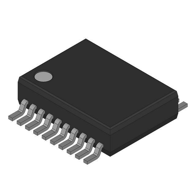


 工商网监
湘ICP备2023018690号
工商网监
湘ICP备2023018690号
