To our customers,
Old Company Name in Catalogs and Other Documents
On April 1st, 2010, NEC Electronics Corporation merged with Renesas Technology
Corporation, and Renesas Electronics Corporation took over all the business of both
companies. Therefore, although the old company name remains in this document, it is a valid
Renesas Electronics document. We appreciate your understanding.
Renesas Electronics website: http://www.renesas.com
April 1st, 2010
Renesas Electronics Corporation
Issued by: Renesas Electronics Corporation (http://www.renesas.com)
Send any inquiries to http://www.renesas.com/inquiry.
�Notice
1.
2.
3.
4.
5.
6.
7.
All information included in this document is current as of the date this document is issued. Such information, however, is
subject to change without any prior notice. Before purchasing or using any Renesas Electronics products listed herein, please
confirm the latest product information with a Renesas Electronics sales office. Also, please pay regular and careful attention to
additional and different information to be disclosed by Renesas Electronics such as that disclosed through our website.
Renesas Electronics does not assume any liability for infringement of patents, copyrights, or other intellectual property rights
of third parties by or arising from the use of Renesas Electronics products or technical information described in this document.
No license, express, implied or otherwise, is granted hereby under any patents, copyrights or other intellectual property rights
of Renesas Electronics or others.
You should not alter, modify, copy, or otherwise misappropriate any Renesas Electronics product, whether in whole or in part.
Descriptions of circuits, software and other related information in this document are provided only to illustrate the operation of
semiconductor products and application examples. You are fully responsible for the incorporation of these circuits, software,
and information in the design of your equipment. Renesas Electronics assumes no responsibility for any losses incurred by
you or third parties arising from the use of these circuits, software, or information.
When exporting the products or technology described in this document, you should comply with the applicable export control
laws and regulations and follow the procedures required by such laws and regulations. You should not use Renesas
Electronics products or the technology described in this document for any purpose relating to military applications or use by
the military, including but not limited to the development of weapons of mass destruction. Renesas Electronics products and
technology may not be used for or incorporated into any products or systems whose manufacture, use, or sale is prohibited
under any applicable domestic or foreign laws or regulations.
Renesas Electronics has used reasonable care in preparing the information included in this document, but Renesas Electronics
does not warrant that such information is error free. Renesas Electronics assumes no liability whatsoever for any damages
incurred by you resulting from errors in or omissions from the information included herein.
Renesas Electronics products are classified according to the following three quality grades: “Standard”, “High Quality”, and
“Specific”. The recommended applications for each Renesas Electronics product depends on the product’s quality grade, as
indicated below. You must check the quality grade of each Renesas Electronics product before using it in a particular
application. You may not use any Renesas Electronics product for any application categorized as “Specific” without the prior
written consent of Renesas Electronics. Further, you may not use any Renesas Electronics product for any application for
which it is not intended without the prior written consent of Renesas Electronics. Renesas Electronics shall not be in any way
liable for any damages or losses incurred by you or third parties arising from the use of any Renesas Electronics product for an
application categorized as “Specific” or for which the product is not intended where you have failed to obtain the prior written
consent of Renesas Electronics. The quality grade of each Renesas Electronics product is “Standard” unless otherwise
expressly specified in a Renesas Electronics data sheets or data books, etc.
“Standard”:
8.
9.
10.
11.
12.
Computers; office equipment; communications equipment; test and measurement equipment; audio and visual
equipment; home electronic appliances; machine tools; personal electronic equipment; and industrial robots.
“High Quality”: Transportation equipment (automobiles, trains, ships, etc.); traffic control systems; anti-disaster systems; anticrime systems; safety equipment; and medical equipment not specifically designed for life support.
“Specific”:
Aircraft; aerospace equipment; submersible repeaters; nuclear reactor control systems; medical equipment or
systems for life support (e.g. artificial life support devices or systems), surgical implantations, or healthcare
intervention (e.g. excision, etc.), and any other applications or purposes that pose a direct threat to human life.
You should use the Renesas Electronics products described in this document within the range specified by Renesas Electronics,
especially with respect to the maximum rating, operating supply voltage range, movement power voltage range, heat radiation
characteristics, installation and other product characteristics. Renesas Electronics shall have no liability for malfunctions or
damages arising out of the use of Renesas Electronics products beyond such specified ranges.
Although Renesas Electronics endeavors to improve the quality and reliability of its products, semiconductor products have
specific characteristics such as the occurrence of failure at a certain rate and malfunctions under certain use conditions. Further,
Renesas Electronics products are not subject to radiation resistance design. Please be sure to implement safety measures to
guard them against the possibility of physical injury, and injury or damage caused by fire in the event of the failure of a
Renesas Electronics product, such as safety design for hardware and software including but not limited to redundancy, fire
control and malfunction prevention, appropriate treatment for aging degradation or any other appropriate measures. Because
the evaluation of microcomputer software alone is very difficult, please evaluate the safety of the final products or system
manufactured by you.
Please contact a Renesas Electronics sales office for details as to environmental matters such as the environmental
compatibility of each Renesas Electronics product. Please use Renesas Electronics products in compliance with all applicable
laws and regulations that regulate the inclusion or use of controlled substances, including without limitation, the EU RoHS
Directive. Renesas Electronics assumes no liability for damages or losses occurring as a result of your noncompliance with
applicable laws and regulations.
This document may not be reproduced or duplicated, in any form, in whole or in part, without prior written consent of Renesas
Electronics.
Please contact a Renesas Electronics sales office if you have any questions regarding the information contained in this
document or Renesas Electronics products, or if you have any other inquiries.
(Note 1) “Renesas Electronics” as used in this document means Renesas Electronics Corporation and also includes its majorityowned subsidiaries.
(Note 2) “Renesas Electronics product(s)” means any product developed or manufactured by or for Renesas Electronics.
�Preliminary User’s Manual
µPD78F9510, 78F9511, 789512
8-bit Single-Chip Microcontrollers
µPD78F9510
µPD78F9511
µPD78F9512
Document No. U18372EJ1V0UD00 (1st edition)
Date Published January 2007 NS CP(K)
©
Printed in Japan
2007
�[MEMO]
2
Preliminary User’s Manual U18372EJ1V0UD
�NOTES FOR CMOS DEVICES
1
VOLTAGE APPLICATION WAVEFORM AT INPUT PIN
Waveform distortion due to input noise or a reflected wave may cause malfunction. If the input of the
CMOS device stays in the area between VIL (MAX) and VIH (MIN) due to noise, etc., the device may
malfunction. Take care to prevent chattering noise from entering the device when the input level is fixed,
and also in the transition period when the input level passes through the area between VIL (MAX) and
VIH (MIN).
2
HANDLING OF UNUSED INPUT PINS
Unconnected CMOS device inputs can be cause of malfunction. If an input pin is unconnected, it is
possible that an internal input level may be generated due to noise, etc., causing malfunction. CMOS
devices behave differently than Bipolar or NMOS devices. Input levels of CMOS devices must be fixed
high or low by using pull-up or pull-down circuitry. Each unused pin should be connected to VDD or GND
via a resistor if there is a possibility that it will be an output pin. All handling related to unused pins must
be judged separately for each device and according to related specifications governing the device.
3
PRECAUTION AGAINST ESD
A strong electric field, when exposed to a MOS device, can cause destruction of the gate oxide and
ultimately degrade the device operation. Steps must be taken to stop generation of static electricity as
much as possible, and quickly dissipate it when it has occurred.
Environmental control must be
adequate. When it is dry, a humidifier should be used. It is recommended to avoid using insulators that
easily build up static electricity. Semiconductor devices must be stored and transported in an anti-static
container, static shielding bag or conductive material. All test and measurement tools including work
benches and floors should be grounded.
The operator should be grounded using a wrist strap.
Semiconductor devices must not be touched with bare hands. Similar precautions need to be taken for
PW boards with mounted semiconductor devices.
4
STATUS BEFORE INITIALIZATION
Power-on does not necessarily define the initial status of a MOS device. Immediately after the power
source is turned ON, devices with reset functions have not yet been initialized. Hence, power-on does
not guarantee output pin levels, I/O settings or contents of registers. A device is not initialized until the
reset signal is received. A reset operation must be executed immediately after power-on for devices
with reset functions.
5
POWER ON/OFF SEQUENCE
In the case of a device that uses different power supplies for the internal operation and external
interface, as a rule, switch on the external power supply after switching on the internal power supply.
When switching the power supply off, as a rule, switch off the external power supply and then the
internal power supply. Use of the reverse power on/off sequences may result in the application of an
overvoltage to the internal elements of the device, causing malfunction and degradation of internal
elements due to the passage of an abnormal current.
The correct power on/off sequence must be judged separately for each device and according to related
specifications governing the device.
6
INPUT OF SIGNAL DURING POWER OFF STATE
Do not input signals or an I/O pull-up power supply while the device is not powered. The current
injection that results from input of such a signal or I/O pull-up power supply may cause malfunction and
the abnormal current that passes in the device at this time may cause degradation of internal elements.
Input of signals during the power off state must be judged separately for each device and according to
related specifications governing the device.
Preliminary User’s Manual U18372EJ1V0UD
3
�Windows, Windows NT, and Windows XP are either registered trademarks or trademarks of Microsoft
Corporation in the United States and/or other countries.
PC/AT is a trademark of International Business Machines Corporation.
HP9000 series 700 and HP-UX are trademarks of Hewlett-Packard Company.
SPARCstation is a trademark of SPARC International, Inc.
Solaris and SunOS are trademarks of Sun Microsystems, Inc.
SuperFlash is a registered trademark of Silicon Storage Technology, Inc. in several countries including the
United States and Japan.
Caution: This product uses SuperFlash® technology licensed from Silicon Storage Technology, Inc.
4
Preliminary User’s Manual U18372EJ1V0UD
�• The information contained in this document is being issued in advance of the production cycle for the
product. The parameters for the product may change before final production or NEC Electronics
Corporation, at its own discretion, may withdraw the product prior to its production.
• Not all products and/or types are available in every country. Please check with an NEC Electronics sales
representative for availability and additional information.
• No part of this document may be copied or reproduced in any form or by any means without the prior written consent
of NEC Electronics. NEC Electronics assumes no responsibility for any errors that may appear in this document.
• NEC Electronics does not assume any liability for infringement of patents, copyrights or other intellectual property
rights of third parties by or arising from the use of NEC Electronics products listed in this document or any other
liability arising from the use of such products. No license, express, implied or otherwise, is granted under any
patents, copyrights or other intellectual property rights of NEC Electronics or others.
• Descriptions of circuits, software and other related information in this document are provided for illustrative purposes
in semiconductor product operation and application examples. The incorporation of these circuits, software and
information in the design of a customer's equipment shall be done under the full responsibility of the customer. NEC
Electronics assumes no responsibility for any losses incurred by customers or third parties arising from the use of
these circuits, software and information.
• While NEC Electronics endeavors to enhance the quality, reliability and safety of NEC Electronics products,
customers agree and acknowledge that the possibility of defects thereof cannot be eliminated entirely. To minimize
risks of damage to property or injury (including death) to persons arising from defects in NEC Electronics products,
customers must incorporate sufficient safety measures in their design, such as redundancy, fire-containment and
anti-failure features.
• NEC Electronics products are classified into the following three quality grades: "Standard", "Special" and "Specific".
The "Specific" quality grade applies only to NEC Electronics products developed based on a customer-designated
"quality assurance program" for a specific application. The recommended applications of an NEC Electronics
products depend on its quality grade, as indicated below. Customers must check the quality grade of each NEC
Electronics product before using it in a particular application.
"Standard": Computers, office equipment, communications equipment, test and measurement equipment, audio and
visual equipment, home electronic appliances, machine tools, personal electronic equipment and
industrial robots.
"Special": Transportation equipment (automobiles, trains, ships, etc.), traffic control systems, anti-disaster
systems, anti-crime systems, safety equipment and medical equipment (not specifically designed for life
support).
"Specific": Aircraft, aerospace equipment, submersible repeaters, nuclear reactor control systems, life support
systems and medical equipment for life support, etc.
The quality grade of NEC Electronics products is "Standard" unless otherwise expressly specified in NEC
Electronics data sheets or data books, etc. If customers wish to use NEC Electronics products in applications
not intended by NEC Electronics, they must contact an NEC Electronics sales representative in advance to
determine NEC Electronics' willingness to support a given application.
(Note)
(1) "NEC Electronics" as used in this statement means NEC Electronics Corporation and also includes its
majority-owned subsidiaries.
(2) "NEC Electronics products" means any product developed or manufactured by or for NEC Electronics (as
defined above).
M5D 02. 11-1
Preliminary User’s Manual U18372EJ1V0UD
5
�INTRODUCTION
Target Readers
This manual is intended for user engineers who wish to understand the functions of
the µPD78F9510, 78F9511, 78F9512 in order to design and develop its application
systems and programs.
Purpose
This manual is intended to give users on understanding of the functions described in
the Organization below.
Organization
Two manuals are available for µPD78F9510, 78F9511, 78F9512: this manual and the
Instruction Manual (common to the 78K0S microcontroller).
µPD78F9510, 78F9511,
78K/0S Series
78F9512
Instructions
User’s Manual
User’s Manual
• Pin functions
• CPU function
• Internal block functions
• Instruction set
• Interrupts
• Instruction description
• Other internal peripheral functions
• Electrical specifications
How to Use This Manual
It is assumed that the readers of this manual have general knowledge of electrical
engineering, logic circuits, and microcontrollers.
◊ To understand the overall functions of µPD78F9510, 78F9511, 78F9512
→ Read this manual in the order of the CONTENTS.
◊ How to read register formats
→ For a bit number enclosed in angle brackets (), the bit name is defined as a
reserved word in the RA78K0S, and is defined as an sfr variable using the
#pragma sfr directive in the CC78K0S.
◊ To learn the detailed functions of a register whose register name is known
→ See APPENDIX C REGISTER INDEX.
◊ To learn the details of the instruction functions of the 78K0S microcontroller
→ Refer to 78K/0S Series Instructions User’s Manual (U11047E) separately
available.
◊ To learn the electrical specifications of the µPD78F9510, 78F9511, 78F9512
→ See CHAPTER 17 ELECTRICAL SPECIFICATIONS (TARGET).
6
Preliminary User’s Manual U18372EJ1V0UD
�Conventions
Data significance:
Higher digits on the left and lower digits on the right
Active low representation: ××× (overscore over pin or signal name)
Note:
Footnote for item marked with Note in the text
Caution:
Information requiring particular attention
Remark:
Supplementary information
Numerical representation: Binary ... ×××× or ××××B
Decimal ... ××××
Hexadecimal ... ××××H
Related Documents
The related documents indicated in this publication may include preliminary versions.
However, preliminary versions are not marked as such.
Documents Related to Devices
Document Name
Document No.
µPD78F9510, 78F9511, 78F9512 User’s Manual
This manual
78K/0S Series Instructions User’s Manual
U11047E
Documents Related to Development Software Tools (User’s Manuals)
Document Name
RA78K0S Assembler Package
Document No.
Operation
U16656E
Language
U14877E
Structured Assembly Language
U11623E
Operation
U16654E
Language
U14872E
ID78K0S-NS Ver. 2.52 Integrated Debugger
Operation
U16584E
ID78K0S-QB Ver. 2.81 Integrated Debugger
Operation
U17287E
CC78K0S C Compiler
PM plus Ver.5.20
U16934E
Documents Related to Development Hardware Tools (User’s Manuals)
Document Name
Document No.
IE-78K0S-NS In-Circuit Emulator
U13549E
IE-78K0S-NS-A In-Circuit Emulator
U15207E
QB-78K0SKX1MINI In-Circuit Emulator
U17272E
Caution
The related documents listed above are subject to change without notice. Be sure to use the latest
version of each document for designing.
Preliminary User’s Manual U18372EJ1V0UD
7
�Documents Related to Flash Memory Writing
Document Name
Document No.
PG-FP4 Flash Memory Programmer User’s Manual
U15260E
PG-FPL2 Flash Memory Programmer User’s Manual
U17307E
Other Related Documents
Document Name
Document No.
SEMICONDUCTOR SELECTION GUIDE - Products and Packages -
X13769X
Semiconductor Device Mount Manual
Note
Quality Grades on NEC Semiconductor Devices
C11531E
NEC Semiconductor Device Reliability/Quality Control System
C10983E
Guide to Prevent Damage for Semiconductor Devices by Electrostatic Discharge (ESD)
C11892E
Note See the “Semiconductor Device Mount Manual” website (http://www.necel.com/pkg/en/mount/index.html).
Caution
The related documents listed above are subject to change without notice. Be sure to use the latest
version of each document for designing.
8
Preliminary User’s Manual U18372EJ1V0UD
�CONTENTS
CHAPTER 1 OVERVIEW......................................................................................................................... 14
1.1
1.2
1.3
1.4
1.5
1.6
Features ...................................................................................................................................... 14
Ordering Information ................................................................................................................. 15
Pin Configuration (Top View) ................................................................................................... 16
78K0S/Kx1+ Product Lineup..................................................................................................... 17
Block Diagram............................................................................................................................ 18
Functional Outline ..................................................................................................................... 19
CHAPTER 2 PIN FUNCTIONS............................................................................................................... 20
2.1
2.2
2.3
Pin Function List........................................................................................................................ 20
Pin Functions ............................................................................................................................. 22
2.2.1
P20 to P23 (Port 2) ....................................................................................................................... 22
2.2.2
P32 and P34 (Port 3) .................................................................................................................... 23
2.2.3
P40 to P47 (Port 4) ....................................................................................................................... 23
2.2.4
RESET .......................................................................................................................................... 23
2.2.5
X1 and X2 ..................................................................................................................................... 23
2.2.6
VDD ................................................................................................................................................ 23
2.2.7
VSS ................................................................................................................................................ 23
Pin I/O Circuits and Connection of Unused Pins ................................................................... 24
CHAPTER 3 CPU ARCHITECTURE...................................................................................................... 26
3.1
3.2
3.3
Memory Space............................................................................................................................ 26
3.1.1
Internal program memory space ................................................................................................... 29
3.1.2
Internal data memory space.......................................................................................................... 30
3.1.3
Special function register (SFR) area ............................................................................................. 30
3.1.4
Data memory addressing .............................................................................................................. 30
Processor Registers .................................................................................................................. 33
3.2.1
Control registers............................................................................................................................ 33
3.2.2
General-purpose registers............................................................................................................. 36
3.2.3
Special function registers (SFRs).................................................................................................. 37
Instruction Address Addressing .............................................................................................. 41
3.3.1
3.4
Relative addressing....................................................................................................................... 41
3.3.2
Immediate addressing ................................................................................................................... 42
3.3.3
Table indirect addressing .............................................................................................................. 42
3.3.4
Register addressing ...................................................................................................................... 43
Operand Address Addressing.................................................................................................. 44
3.4.1
Direct addressing .......................................................................................................................... 44
3.4.2
Short direct addressing ................................................................................................................. 45
3.4.3
Special function register (SFR) addressing ................................................................................... 46
3.4.4
Register addressing ...................................................................................................................... 47
3.4.5
Register indirect addressing.......................................................................................................... 48
Preliminary User’s Manual U18372EJ1V0UD
9
�3.4.6
Based addressing..........................................................................................................................49
3.4.7
Stack addressing ...........................................................................................................................50
CHAPTER 4 PORT FUNCTIONS ...........................................................................................................51
4.1
4.2
4.3
4.4
Functions of Ports .....................................................................................................................51
Port Configuration .....................................................................................................................52
4.2.1
Port 2.............................................................................................................................................52
4.2.2
Port 3.............................................................................................................................................56
4.2.3
Port 4.............................................................................................................................................57
Registers Controlling Port Functions ......................................................................................58
Operation of Port Function .......................................................................................................62
4.4.1
Writing to I/O port ..........................................................................................................................62
4.4.2
Reading from I/O port ....................................................................................................................62
4.4.3
Operations on I/O port ...................................................................................................................62
CHAPTER 5 CLOCK GENERATORS...................................................................................................63
5.1
5.2
5.3
5.4
5.5
5.6
Functions of Clock Generators ................................................................................................63
5.1.1
System clock oscillators ................................................................................................................63
5.1.2
Clock oscillator for interval time generation ...................................................................................63
Configuration of Clock Generators ..........................................................................................64
Registers Controlling Clock Generators .................................................................................66
System Clock Oscillators ..........................................................................................................69
5.4.1
High-speed internal oscillator ........................................................................................................69
5.4.2
Crystal/ceramic oscillator...............................................................................................................69
5.4.3
External clock input circuit .............................................................................................................71
5.4.4
Prescaler .......................................................................................................................................71
Operation of CPU Clock Generator ..........................................................................................72
Operation of Clock Generator Supplying Clock to Peripheral Hardware.............................78
CHAPTER 6 16-BIT TIMER/EVENT COUNTER 00 .............................................................................80
6.1
6.2
6.3
6.4
6.5
Functions of 16-bit Timer/Event Counter 00 ...........................................................................80
Configuration of 16-bit Timer/Event Counter 00 .....................................................................81
Registers to Control 16-bit Timer/Event Counter 00 ..............................................................85
Operation of 16-bit Timer/Event Counter 00............................................................................91
6.4.1
Interval timer operation..................................................................................................................91
6.4.2
External event counter operation...................................................................................................93
6.4.3
Pulse width measurement operations............................................................................................96
6.4.4
Square-wave output operation.....................................................................................................104
6.4.5
PPG output operations ................................................................................................................106
6.4.6
One-shot pulse output operation .................................................................................................109
Cautions Related to 16-bit Timer/Event Counter 00 .............................................................114
CHAPTER 7 8-BIT TIMER H1 .............................................................................................................121
7.1
10
Functions of 8-bit Timer H1.....................................................................................................121
Preliminary User’s Manual U18372EJ1V0UD
�7.2
7.3
7.4
Configuration of 8-bit Timer H1..............................................................................................121
Registers Controlling 8-bit Timer H1 .....................................................................................124
Operation of 8-bit Timer H1 .................................................................................................... 126
7.4.1
Operation as interval timer/square-wave output .......................................................................... 126
7.4.2
Operation as PWM output mode ................................................................................................. 129
CHAPTER 8 WATCHDOG TIMER .......................................................................................................135
8.1
8.2
8.3
8.4
Functions of Watchdog Timer ................................................................................................135
Configuration of Watchdog Timer..........................................................................................137
Registers Controlling Watchdog Timer .................................................................................138
Operation of Watchdog Timer ................................................................................................140
8.4.1
Watchdog timer operation when “low-speed internal oscillator cannot be stopped” is
selected by option byte................................................................................................................ 140
8.4.2
Watchdog timer operation when “low-speed internal oscillator can be stopped by
software” is selected by option byte ............................................................................................ 142
8.4.3
Watchdog timer operation in STOP mode (when “low-speed internal oscillator can be
stopped by software” is selected by option byte)......................................................................... 144
8.4.4
Watchdog timer operation in HALT mode (when “low-speed internal oscillator can be
stopped by software” is selected by option byte)......................................................................... 145
CHAPTER 9 INTERRUPT FUNCTIONS .............................................................................................. 146
9.1
9.2
9.3
9.4
Interrupt Function Types.........................................................................................................146
Interrupt Sources and Configuration.....................................................................................146
Interrupt Function Control Registers.....................................................................................148
Interrupt Servicing Operation.................................................................................................151
9.4.1
Maskable interrupt request acknowledgment operation .............................................................. 151
9.4.2
Multiple interrupt servicing........................................................................................................... 153
9.4.3
Interrupt request pending ............................................................................................................ 155
CHAPTER 10 STANDBY FUNCTION..................................................................................................156
10.1 Standby Function and Configuration ....................................................................................156
10.1.1
Standby function ......................................................................................................................... 156
10.1.2
Registers used during standby.................................................................................................... 158
10.2 Standby Function Operation ..................................................................................................159
10.2.1
HALT mode ................................................................................................................................. 159
10.2.2
STOP mode ................................................................................................................................ 162
CHAPTER 11 RESET FUNCTION .......................................................................................................166
11.1 Register for Confirming Reset Source ..................................................................................173
CHAPTER 12 POWER-ON-CLEAR CIRCUIT .....................................................................................174
12.1 Functions of Power-on-Clear Circuit .....................................................................................174
12.2 Configuration of Power-on-Clear Circuit...............................................................................175
12.3 Operation of Power-on-Clear Circuit .....................................................................................175
Preliminary User’s Manual U18372EJ1V0UD
11
�12.4 Cautions for Power-on-Clear Circuit......................................................................................176
CHAPTER 13 LOW-VOLTAGE DETECTOR .......................................................................................178
13.1
13.2
13.3
13.4
13.5
Functions of Low-Voltage Detector .......................................................................................178
Configuration of Low-Voltage Detector .................................................................................178
Registers Controlling Low-Voltage Detector ........................................................................179
Operation of Low-Voltage Detector........................................................................................181
Cautions for Low-Voltage Detector........................................................................................185
CHAPTER 14 OPTION BYTE................................................................................................................188
14.1 Functions of Option Byte ........................................................................................................188
14.2 Format of Option Byte .............................................................................................................189
14.3 Caution When the RESET Pin Is Used as an Input-Only Port Pin (P34).............................190
CHAPTER 15 FLASH MEMORY ..........................................................................................................191
15.1
15.2
15.3
15.4
15.5
15.6
Features ....................................................................................................................................191
Memory Configuration.............................................................................................................192
Functional Outline....................................................................................................................192
Writing with Flash Memory Programmer...............................................................................193
Programming Environment.....................................................................................................194
Processing of Pins on Board ..................................................................................................196
15.6.1
X1 and X2 pins ............................................................................................................................196
15.6.2
RESET pin...................................................................................................................................197
15.6.3
Port pins ......................................................................................................................................198
15.6.4
Power supply...............................................................................................................................198
15.7 On-Board and Off-Board Flash Memory Programming .......................................................199
15.7.1
Flash memory programming mode..............................................................................................199
15.7.2
Communication commands .........................................................................................................199
15.7.3
Security settings ..........................................................................................................................200
15.8 Flash Memory Programming by Self Writing ........................................................................201
15.8.1
Outline of self programming ........................................................................................................201
15.8.2
Cautions on self programming function .......................................................................................204
15.8.3
Registers used for self programming function .............................................................................204
15.8.4
Example of shifting normal mode to self programming mode ......................................................211
15.8.5
Example of shifting self programming mode to normal mode ......................................................214
15.8.6
Example of block erase operation in self programming mode .....................................................217
15.8.7
Example of block blank check operation in self programming mode ...........................................220
15.8.8
Example of byte write operation in self programming mode ........................................................223
15.8.9
Example of internal verify operation in self programming mode ..................................................226
15.8.10 Examples of operation when command execution time should be minimized in
self programming mode..............................................................................................................230
15.8.11 Examples of operation when interrupt-disabled time should be minimized in
self programming mode...............................................................................................................237
12
Preliminary User’s Manual U18372EJ1V0UD
�CHAPTER 16 INSTRUCTION SET OVERVIEW.................................................................................248
16.1 Operation ..................................................................................................................................248
16.1.1
Operand identifiers and description methods .............................................................................. 248
16.1.2
Description of “Operation” column............................................................................................... 249
16.1.3
Description of “Flag” column ....................................................................................................... 249
16.2 Operation List...........................................................................................................................250
16.3 Instructions Listed by Addressing Type ...............................................................................255
CHAPTER 17 ELECTRICAL SPECIFICATIONS (TARGET)...............................................................258
CHAPTER 18 PACKAGE DRAWING ..................................................................................................269
CHAPTER 19 RECOMMENDED SOLDERING CONDITIONS ..........................................................270
APPENDIX A DEVELOPMENT TOOLS ..............................................................................................271
A.1
A.2
A.3
A.4
A.5
A.6
Software Package ....................................................................................................................276
Language Processing Software .............................................................................................276
Control Software ......................................................................................................................277
Flash Memory Writing Tools...................................................................................................277
Debugging Tools (Hardware)..................................................................................................278
A.5.1
When using in-circuit emulator QB-78K0SKX1 ........................................................................... 278
A.5.2
When using in-circuit emulator QB-MINI2 ................................................................................... 278
A.5.3
When using in-circuit emulator IE-78K0S-NS or IE-78K0S-NS-A ............................................... 279
A.5.4
When using in-circuit emulator QB-78K0SKX1MINI.................................................................... 279
Debugging Tools (Software)...................................................................................................280
APPENDIX B NOTES ON TARGET SYSTEM DESIGN...................................................................281
APPENDIX C REGISTER INDEX.........................................................................................................284
C.1
C.2
Register Index (Register Name) .............................................................................................284
Register Index (Symbol)..........................................................................................................286
APPENDIX D LIST OF CAUTIONS.....................................................................................................288
Preliminary User’s Manual U18372EJ1V0UD
13
�CHAPTER 1 OVERVIEW
1.1 Features
O 78K0S CPU core
O ROM and RAM capacities
Item
Program Memory (Flash Memory)
Memory (Internal High-Speed RAM)
Part number
µPD78F9510
1 KB
µPD78F9511
2 KB
µPD78F9512
4 KB
128 bytes
O Minimum instruction execution time: 0.2 µs (with 10 MHz@4.0 to 5.5 V operation)
O Clock
• High-speed system clock … Selected from the following two sources
- Ceramic/crystal resonator:
1 to 10 MHz
- High-speed internal oscillator:
8 MHz ±3% (−10 to +70°C), 8 MHz ±5% (−40 to +85°C)
• Low-speed internal oscillator 240 kHz (TYP.) … Watchdog timer, timer clock in intermittent operation
O I/O ports: 14 (CMOS I/O: 13, CMOS input: 1)
O Timer: 3 channels
• 16-bit timer/event counter:
1 channel … Timer output × 1, capture input × 2
• 8-bit timer:
1 channel … PWM output × 1
• Watchdog timer:
1 channel … Operable with low-speed internal oscillation clock
O On-chip power-on-clear (POC) circuit (A reset is automatically generated when the voltage drops to 2.1 V ±0.1 V
or below)
O On-chip low voltage detector (LVI) circuit (An interrupt/reset (selectable) is generated when the detection voltage
is reached)
• Detection voltage: Selectable from ten levels between 2.35 and 4.3 V
O Single-power-supply flash memory
• Flash self programming enabled
• Software protection function: Protected from outside party copying (no flash reading command)
• Time required for writing by dedicated flash memory programmer: Approximately 3 seconds (4 KB)
∗ Write operations on mass production lines supported
O Safety function
• Watchdog timer operated by clock independent from CPU
… A hang-up can be detected even if the system clock stops
• Supply voltage drop detectable by LVI
… Appropriate processing can be executed before the supply voltage drops below the operation voltage
• Equipped with option byte function
… Important system operation settings set in hardware
O Assembly and C language supported
O Enhanced development environment
• Support for full-function emulator (IECUBE), simplified emulator (MINICUBE2), and simulator
O Supply voltage: VDD = 2.0 to 5.5 V
∗ Use this product in a voltage range of 2.2 to 5.5 V because the detection voltage (VPOC) of the power-on-clear
(POC) circuit is 2.1 V ±0.1 V.
O Operating temperature range: TA = −40 to +85°C
14
Preliminary User’s Manual U18372EJ1V0UD
�CHAPTER 1 OVERVIEW
1.2 Ordering Information
Part Number
µPD78F9 ××× - ×× (×) - ××× -A
Semiconductor component
-A
Lead-free
Quality grades
Blank
Standard
Package type
GR-JJG
Plastic SSOP (5.25 mm (225))
Number of pins
High-speed RAM
Flash memory
510
16 pins
128 bytes
1 K bytes
511
16 pins
128 bytes
2 K bytes
512
16 pins
128 bytes
4 K bytes
Product type
F
Flash memory versions
[Part number list]
µPD78F9510GR-JJG-ANote
µPD78F9511GR-JJG-ANote
µPD78F9512GR-JJG-ANote
Note Under development
Preliminary User’s Manual U18372EJ1V0UD
15
�CHAPTER 1 OVERVIEW
1.3 Pin Configuration (Top View)
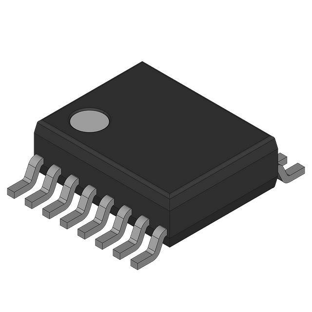
16-pin plastic SSOP
INTP0, INTP1:
16
P20/TI000/TOH1
1
16
P21/TI010/TO00/INTP0
P41
2
15
P42
P40
3
14
P43
VSS
4
13
P32/INTP1
VDD
5
12
P34/RESET
P47
6
11
P44
P46
7
10
P23/X1
8
9
External interrupt input
TI000, TI010:
P45
P22/X2
Timer input
P20 to P23:
Port 2
TO00, TOH1:
Timer output
P32, P34:
Port 3
VDD:
Power supply
P40 to P47:
Port 4
VSS:
Ground
RESET:
Reset
X1, X2:
Crystal oscillator (X1 input clock)
Preliminary User’s Manual U18372EJ1V0UD
�CHAPTER 1 OVERVIEW
1.4 78K0S/Kx1+ Product Lineup
The following table shows the product lineup of the 78K0S/Kx1+.
Part Number
78K0S/KU1+
78K0S/KY1+
78K0S/KA1+
78K0S/KB1+
10 pins
16 pins
20 pins
30 pins
Item
Number of pins
Internal
Flash memory
memory
1 KB, 2 KB, 4 KB
RAM
2 KB
4 KB
4 KB, 8 KB
128
256
256 bytes
bytes
bytes
128 bytes
VDD = 2.0 to 5.5 V
Supply voltage
Note 1
Minimum instruction
0.20 µs (10 MHz, VDD = 4.0 to 5.5 V)
execution time
0.33 µs (6 MHz, VDD = 3.0 to 5.5 V)
0.40 µs (5 MHz, VDD = 2.7 to 5.5 V)
1.0 µs (2 MHz, VDD = 2.0 to 5.5 V)
High-speed internal oscillation (8 MHz (TYP.))
Note 4
Crystal/ceramic oscillation (1 to 10 MHz)
System clock
(oscillation frequency)
External clock input oscillation (1 to 10 MHz)
Clock for TMH1 and WDT
Low-speed internal oscillation (240 kHz (TYP.))
(oscillation frequency)
Port
Timer
CMOS I/O
7
13
15
24
CMOS input
1
1
1
1
CMOS output
−
−
1
1
1 ch
16-bit (TM0)
8-bit (TMH)
1 ch
−
8-bit (TM8)
1 ch
WDT
1 ch
−
Serial interface
LIN-Bus-supporting UART: 1 ch
Note 2
Note 2
A/D converter
10 bits: 4 ch (2.7 to 5.5 V)
Multiplier (8 bits × 8 bits)
Interrupts
−
External
5
4
Note 3
RESET pin
9
Provided
2.1 V ±0.1 V
POC
LVI
Provided (selectable by software)
WDT
Operating temperature range
Provided
2
Internal
Reset
Note 4
Provided
Standard products:
−40 to +85°C
Standard products, (A) grade products: −40 to +85°C
(A2) grade products: −40 to +125°C
Note 1. Use this product in a voltage range of 2.2 to 5.5 V because the detection voltage (VPOC) of the power-onclear (POC) circuit is 2.1 V ±0.1 V.
2. The product without A/D converter (µ PD78F95xx) is provided for the 78K0S/KU1+ (under development)
and 78K0S/KY1+ respectively. This product has no A/D converter.
3. 4 factors for products without A/D converter
4. The product without A/D converter (µ PD78F950x) in the 78K0S/KU1+ (under development) is not
supported.
Preliminary User’s Manual U18372EJ1V0UD
17
�CHAPTER 1 OVERVIEW
1.5 Block Diagram
TO00/TI010/P21
TI000/P20
Port 2
16-bit timer/
event counter 00
4
P32
Port 3
TOH1/P20
8-bit timer H1
78K0S
CPU
core
P20 to P23
P34
Flash
memory
Port 4
8
P40 to P47
Low-speed
internal
oscillator
Power on clear/
low voltage
indicator
Watchdog
timer
Internal
high-speed
RAM
INTP0/P21
INTP1/P32
POC/LVI
control
Reset control
Interrupt
control
System
control
RESET/P34
X1/P23
X2/P22
VDD
18
VSS
Preliminary User’s Manual U18372EJ1V0UD
High-speed
internal
oscillator
�CHAPTER 1 OVERVIEW
1.6 Functional Outline
µPD78F9510
Item
Internal
memory
Flash memory
1 KB
High-speed RAM
128 bytes
µPD78F9511
2 KB
Memory space
64 KB
X1 input clock (oscillation frequency)
Crystal/ceramic/external clock input:
µPD78F9512
4 KB
10 MHz (VDD = 2.0 to 5.5 V)
Internal
High speed (oscillation
oscillation
frequency)
clock
Low speed (for TMH1
Internal oscillation: 8 MHz (TYP.)
Internal oscillation: 240 kHz (TYP.)
and WDT)
General-purpose registers
8 bits × 8 registers
Instruction execution time
0.2 µs/0.4 µs/0.8 µs/1.6 µs/3.2 µs (X1 input clock: fX = 10 MHz)
I/O port
Total:
Timer
Vectored
interrupt sources
14 pins
CMOS I/O:
13 pins
CMOS input:
1 pin
• 16-bit timer/event counter:
1 channel
• 8-bit timer (timer H1):
1 channel
• Watchdog timer:
1 channel
Timer output
2 pins (PWM: 1 pin)
External
2
Internal
4
• Reset by RESET pin
• Internal reset by watchdog timer
• Internal reset by power-on-clear
Reset
• Internal reset by low-voltage detector
Note
Supply voltage
VDD = 2.0 to 5.5 V
Operating temperature range
−40 to +85°C
Package
16-pin plastic SSOP
Note
Use this product in a voltage range of 2.2 to 5.5 V because the detection voltage (VPOC) of the power-on-clear
(POC) circuit is 2.1 V ±0.1 V.
Preliminary User’s Manual U18372EJ1V0UD
19
�CHAPTER 2 PIN FUNCTIONS
2.1 Pin Function List
(1) Port pins
Pin Name
I/O
Function
After Reset
Alternate-Function
Pin
I/O
P20
Port 2.
Input
4-bit I/O port.
P21
TI010/TO00/
Can be set to input or output mode in 1-bit units.
P22
Note
P23
Note
TI000/TOH1
INTP0
An on-chip pull-up resistor can be connected by setting
software.
P32
I/O
Port 3
Can be set to input or output mode in
X2
Note
X1
Note
Input
INTP1
Input
RESET
1-bit units.
An on-chip pull-up resistor can be
connected by setting software.
P34
Note
Input
P40 to P47
I/O
Input only
Port 4.
Input
8-bit I/O port.
Can be set to input or output mode in 1-bit units.
An on-chip pull-up resistor can be connected by setting
software.
Note
For the setting method for pin functions, see CHAPTER 14 OPTION BYTE.
Caution The P22/X2 and P23/X1 pins are pulled down during reset.
20
Preliminary User’s Manual U18372EJ1V0UD
Note
−
�CHAPTER 2 PIN FUNCTIONS
(2) Non-port pins
Pin Name
I/O
Function
After Reset
AlternateFunction Pin
INTP0
Input
External interrupt input for which the valid edge (rising edge,
Input
P21 /TI010/
TO00
falling edge, or both rising and falling edges) can be specified
INTP1
P32
Input
TI000
External count clock input to 16-bit timer/event counter 00.
Input
P20 /TOH1
Capture trigger input to capture registers (CR000 and CR010) of
16-bit timer/event counter 00
TI010
TO00
Output
Capture trigger input to capture register (CR000) of 16-bit
P21/TO00/
timer/event counter 00
INTP0
16-bit timer/event counter 00 output
Input
P21/TI010/
INTP0
TOH1
RESET
X1
Note
Note
Output
8-bit timer H1 output
Input
P20/TI000
Input
System reset input
Input
P34
Note
Input
Connection of crystal/ceramic oscillator for system clock
−
P23
Note
−
P22
Note
oscillation.
External clock input
X2
Note
−
Connection of crystal/ceramic oscillator for system clock
oscillation.
VDD
−
Positive power supply
−
−
VSS
−
Ground potential
−
−
Note
For the setting method for pin functions, see CHAPTER 14 OPTION BYTE.
Caution The P22/X2 and P23/X1 pins are pulled down during reset.
Preliminary User’s Manual U18372EJ1V0UD
21
�CHAPTER 2 PIN FUNCTIONS
2.2 Pin Functions
2.2.1 P20 to P23 (Port 2)
P20 to P23 constitute a 4-bit I/O port. In addition to the function as I/O port pins, these pins also have a function to
input/output a timer signal, and input an external interrupt request signal.
P22 and P23 also function as the X2 and X1, respectively. For the setting method for pin functions, see CHAPTER
14 OPTION BYTE.
These pins can be set to the following operation modes in 1-bit units.
(1) Port mode
P20 to P23 function as a 4-bit I/O port. Each bit of this port can be set to the input or output mode by using
port mode register 2 (PM2). In addition, an on-chip pull-up resistor can be connected to the port by using pullup resistor option register 2 (PU2).
(2) Control mode
P20 to P23 function to input/output a timer signal, and input an external interrupt request signal.
(a) TI000
This pin inputs an external count clock to 16-bit timer/event counter 00, or a capture trigger signal to the
capture registers (CR000 and CR010) of 16-bit timer/event counter 00.
(b) TI010
This pin inputs a capture trigger signal to the capture register (CR000) of 16-bit timer/event counter 00.
(c) TO00
This pin outputs a signal from 16-bit timer/event counter 00.
(d) TOH1
This pin outputs a signal from 8-bit timer H1.
(e) INTP0
This is an external interrupt request input pin for which the valid edge (rising edge, falling edge, or both
rising and falling edges) can be specified.
Caution
22
The P22/X2 and P23/X1 pins are pulled down during reset.
Preliminary User’s Manual U18372EJ1V0UD
�CHAPTER 2 PIN FUNCTIONS
2.2.2 P32 and P34 (Port 3)
P32 is a 1-bit I/O port. In addition to the function as an I/O port pin, this pin also has a function to input an external
interrupt request signal.
P34 is a 1-bit input-only port. This pin is also used as a RESET pin, and when the power is turned on, this is the
reset function.
For the setting method for pin functions, see CHAPTER 14 OPTION BYTE.
When P34 is used as an input port pin, connect the pull-up resistor.
P32 and P34 can be set to the following operation modes in 1-bit units.
(1) Port mode
P32 functions as a 1-bit I/O port. This pin can be set to the input or output mode by using port mode register 3
(PM3). In addition, an on-chip pull-up resistor can be connected to the port by using pull-up resistor option
register 3 (PU3).
P34 functions as a 1-bit input-only port.
(2) Control mode
P32 functions as an external interrupt request input pin (INTP1) for which the valid edge (rising edge, falling
edge, or both rising and falling edges) can be specified.
2.2.3 P40 to P47 (Port 4)
P40 to P47 constitute an 8-bit I/O port. Each bit of this port can be set to the input or output mode by using port
mode register 4 (PM4). In addition, an on-chip pull-up resistor can be connected to the port by using pull-up resistor
option register 4 (PU4).
2.2.4 RESET
This pin inputs an active-low system reset signal.
When the power is turned on, this is the reset function,
regardless of the option byte setting.
2.2.5 X1 and X2
These pins connect an oscillator to oscillate the X1 input clock.
X1 and X2 also function as the P23 and P22, respectively. For the setting method for pin functions, see CHAPTER
14 OPTION BYTE.
Supply an external clock to X1.
Caution The P22/X2 and P23/X1 pins are pulled down during reset.
2.2.6 VDD
This is the positive power supply pin.
2.2.7 VSS
This is the ground pin.
Be sure to connect VSS to a stabilized GND (= 0 V).
Preliminary User’s Manual U18372EJ1V0UD
23
�CHAPTER 2 PIN FUNCTIONS
2.3 Pin I/O Circuits and Connection of Unused Pins
Table 2-1 shows I/O circuit type of each pin and the connections of unused pins.
For the configuration of the I/O circuit of each type, refer to Figure 2-1.
Table 2-1. Types of Pin I/O Circuits and Connection of Unused Pins
Pin Name
P20/TI000/TOH1
I/O Circuit Type
11-H
I/O
I/O
36-A
Input:
Individually connect to VDD or VSS via resistor.
Individually connect to VSS via resistor.
Output: Leave open.
P23/X1
P32/INTP1
Input:
Output: Leave open.
P21/TI010/TO00/INTP0
P22/X2
Recommended Connection of Unused Pin
8-A
Input:
Individually connect to VDD or VSS via resistor.
Output: Leave open.
P34/RESET
2
Input
P40 to P47
8-A
I/O
Connect to VDD via resistor.
Input:
Individually connect to VDD or VSS via resistor.
Output: Leave open.
24
Preliminary User’s Manual U18372EJ1V0UD
�CHAPTER 2 PIN FUNCTIONS
Figure 2-1. Pin I/O Circuits
Type 36-A
Type 2
Feedback
cut-off
IN
P-ch
Schmitt-triggered input with hysteresis characteristics
X1,
IN/OUT
OSC
enable
X2,
IN/OUT
Type 8-A
VDD
VDD
Pull up
enable
P-ch
VDD
Pull up
enable
P-ch
Data
P-ch
Output
disable
N-ch
VDD
Data
VSS
P-ch
IN/OUT
Output
disable
N-ch
VDD
Pull up
enable
P-ch
VDD
Data
P-ch
Output
disable
N-ch
Type 11-H
VDD
VSS
Pull up
enable
P-ch
VDD
Data
P-ch
IN/OUT
Output
disable
N-ch
VSS
Input
enable
Preliminary User’s Manual U18372EJ1V0UD
25
�CHAPTER 3 CPU ARCHITECTURE
3.1
Memory Space
The µPD78F9510, 78F9511, 78F9512 can access up to 64 KB of memory space. Figures 3-1 to 3-3 show the
memory maps.
Figure 3-1. Memory Map (µPD78F9510)
FFFFH
Special function registers
(SFR)
256 × 8 bits
FF00H
FEFFH
Internal high-speed RAM
128 × 8 bits
FE80H
FE7FH
Use prohibited
Data memory
space
03FFH
0400H
03FFH
Program area
Program memory
space
Flash memory
1,024 × 8 bits
0
0
0
0
082
081
080
07F
H
H
H
H
Protect byte area
Option byte area
CALLT table area
0040H
003FH
Program area
0014H
0013H
Vector table area
0000H
0000H
Remark
26
The option byte and protect byte are 1 byte each.
Preliminary User’s Manual U18372EJ1V0UD
�CHAPTER 3 CPU ARCHITECTURE
Figure 3-2. Memory Map (µPD78F9511)
FFFFH
Special function registers
(SFR)
256 × 8 bits
FF00H
FEFFH
Internal high-speed RAM
128 × 8 bits
FE80H
FE7FH
Use prohibited
Data memory
space
07FFH
0800H
07FFH
Program area
Program memory
space
Flash memory
2,048 × 8 bits
0
0
0
0
082
081
080
07F
H
H
H
H
Protect byte area
Option byte area
CALLT table area
0040H
003FH
Program area
0014H
0013H
Vector table area
0000H
0000H
Remark
The option byte and protect byte are 1 byte each.
Preliminary User’s Manual U18372EJ1V0UD
27
�CHAPTER 3 CPU ARCHITECTURE
Figure 3-3. Memory Map (µPD78F9512)
FFFFH
Special function registers
(SFR)
256 × 8 bits
FF00H
FEFFH
Internal high-speed RAM
128 × 8 bits
FE80H
FE7FH
Use prohibited
Data memory
space
0FFFH
1000H
0FFFH
Program area
Program memory
space
Flash memory
4,096 × 8 bits
0
0
0
0
082
081
080
07F
H
H
H
H
Protect byte area
Option byte area
CALLT table area
0040H
003FH
Program area
0014H
0013H
Vector table area
0000H
0000H
Remark
28
The option byte and protect byte are 1 byte each.
Preliminary User’s Manual U18372EJ1V0UD
�CHAPTER 3 CPU ARCHITECTURE
3.1.1 Internal program memory space
The internal program memory space stores programs and table data. This space is usually addressed by the
program counter (PC).
The µPD78F9510, 78F9511, 78F9512 provide the following internal ROMs (or flash memory) containing the
following capacities.
Table 3-1. Internal ROM Capacity
Part Number
Internal ROM
Structure
µPD78F9510
Capacity
1,024 × 8 bits
Flash memory
µPD78F9511
2,048 × 8 bits
µPD78F9512
4,096 × 8 bits
The following areas are allocated to the internal program memory space.
(1)
Vector table area
The 20-byte area of addresses 0000H to 0013H is reserved as a vector table area. This area stores program
start addresses to be used when branching by RESET or interrupt request generation.
Of a
16-bit address, the lower 8 bits are stored in an even address, and the higher 8 bits are stored in an odd
address.
Table 3-2. Vector Table
Vector Table Address
Interrupt Request
Vector Table Address
Interrupt Request
0000H
Reset
000CH
INTTMH1
0006H
INTLVI
000EH
INTTM000
0008H
INTP0
0010H
INTTM010
000AH
INTP1
(2)
CALLT instruction table area
The subroutine entry address of a 1-byte call instruction (CALLT) can be stored in the 64-byte area of
addresses 0040H to 007FH.
(3)
Option byte area
The option byte area is the 1-byte area of address 0080H. For details, refer to CHAPTER 14 OPTION
BYTE.
(4)
Protect byte area
The protect byte area is the 1-byte area of address 0081H. For details, refer to CHAPTER 15 FLASH
MEMORY.
Preliminary User’s Manual U18372EJ1V0UD
29
�CHAPTER 3 CPU ARCHITECTURE
3.1.2 Internal data memory space
128-byte internal high-speed RAM is provided in the µPD78F9510, 78F9511, 78F9512.
The internal high-speed RAM can also be used as a stack memory.
3.1.3 Special function register (SFR) area
Special function registers (SFRs) of on-chip peripheral hardware are allocated to the area of FF00H to FFFFH (see
Table 3-3).
3.1.4 Data memory addressing
The µPD78F9510, 78F9511, 78F9512 are provided with a wide range of addressing modes to make memory
manipulation as efficient as possible. The area (FE80H to FEFFH) which contains a data memory and the special
function register (SFR) area can be accessed using a unique addressing mode in accordance with each function.
Figures 3-4 to 3-6 illustrate the data memory addressing.
Figure 3-4. Data Memory Addressing (µPD78F9510)
FFFFH
Special function registers (SFR)
256 × 8 bits
SFR addressing
FF20H
FF1FH
FF00H
FEFFH
Short direct addressing
Internal high-speed RAM
128 × 8 bits
FE80H
FE7FH
Direct addressing
Register indirect addressing
Based addressing
Use prohibited
0400H
03FFH
Flash memory
1,024 × 8 bits
0000H
30
Preliminary User’s Manual U18372EJ1V0UD
�CHAPTER 3 CPU ARCHITECTURE
Figure 3-5. Data Memory Addressing (µPD78F9511)
FFFFH
Special function registers (SFR)
256 × 8 bits
SFR addressing
FF20H
FF1FH
FF00H
FEFFH
Short direct addressing
Internal high-speed RAM
128 × 8 bits
FE80H
FE7FH
Direct addressing
Register indirect addressing
Based addressing
Use prohibited
0800H
07FFH
Flash memory
2,048 × 8 bits
0000H
Preliminary User’s Manual U18372EJ1V0UD
31
�CHAPTER 3 CPU ARCHITECTURE
Figure 3-6. Data Memory Addressing (µPD78F9512)
FFFFH
Special function registers (SFR)
256 × 8 bits
SFR addressing
FF20H
FF1FH
FF00H
FEFFH
Short direct addressing
Internal high-speed RAM
128 × 8 bits
FE80H
FE7FH
Direct addressing
Register indirect addressing
Based addressing
Use prohibited
1000H
0FFFH
Flash memory
4,096 × 8 bits
0000H
32
Preliminary User’s Manual U18372EJ1V0UD
�CHAPTER 3 CPU ARCHITECTURE
3.2
Processor Registers
The µPD78F9510, 78F9511, 78F9512 provide the following on-chip processor registers.
3.2.1 Control registers
The control registers have special functions to control the program sequence statuses and stack memory. The
control registers include a program counter, a program status word, and a stack pointer.
(1) Program counter (PC)
The program counter is a 16-bit register which holds the address information of the next program to be
executed.
In normal operation, the PC is automatically incremented according to the number of bytes of the instruction to
be fetched. When a branch instruction is executed, immediate data or register contents are set.
Reset signal generation sets the reset vector table values at addresses 0000H and 0001H to the program
counter.
Figure 3-7. Program Counter Configuration
15
0
PC PC15 PC14 PC13 PC12 PC11 PC10 PC9
PC8
PC7
PC6
PC5
PC4
PC3
PC2
PC1
PC0
(2) Program status word (PSW)
The program status word is an 8-bit register consisting of various flags to be set/reset by instruction execution.
Program status word contents are stored in stack area upon interrupt request generation or PUSH PSW
instruction execution and are restored upon execution of the RETI and POP PSW instructions.
Reset signal generation sets PSW to 02H.
Figure 3-8. Program Status Word Configuration
7
PSW
IE
0
Z
0
AC
0
0
Preliminary User’s Manual U18372EJ1V0UD
1
CY
33
�CHAPTER 3 CPU ARCHITECTURE
(a) Interrupt enable flag (IE)
This flag controls interrupt request acknowledge operations of the CPU.
When IE = 0, the interrupt disabled (DI) status is set. All interrupt requests are disabled.
When IE = 1, the interrupt enabled (EI) status is set. Interrupt request acknowledgment is controlled with
an interrupt mask flag for various interrupt sources.
This flag is reset to 0 upon DI instruction execution or interrupt acknowledgment and is set to 1 upon EI
instruction execution.
(b) Zero flag (Z)
When the operation result is zero, this flag is set to 1. It is reset to 0 in all other cases.
(c) Auxiliary carry flag (AC)
If the operation result has a carry from bit 3 or a borrow at bit 3, this flag is set to 1. It is reset to 0 in all
other cases.
(d) Carry flag (CY)
This flag stores overflow and underflow that have occurred upon add/subtract instruction execution. It
stores the shift-out value upon rotate instruction execution and functions as a bit accumulator during bit
operation instruction execution.
(3) Stack pointer (SP)
This is a 16-bit register to hold the start address of the memory stack area. Only the internal high-speed RAM
area can be set as the stack area (Other than the internal high-speed RAM area cannot be set as the stack
area).
Figure 3-9. Stack Pointer Configuration
15
0
SP SP15 SP14 SP13 SP12 SP11 SP10 SP9
SP8
SP7
SP6
SP5
SP4
SP3
SP2
SP1
SP0
The SP is decremented before writing (saving) to the stack memory and is incremented after reading
(restoring) from the stack memory.
Each stack operation saves/restores data as shown in Figures 3-10 and 3-11.
Cautions 1. Since reset signal generation makes the SP contents undefined, be sure to initialize the
SP before using the stack memory.
2. Stack pointers can be set only to the high-speed RAM area, and only the lower 10 bits
can be actually set.
Thus, if the stack pointer is specified to 0FF00H, it is converted to 0FB00H in the highspeed RAM area, since 0FF00H is in the SFR area and not in the high-speed RAM area.
When the value is actually pushed onto the stack, 1 is subtracted from 0FB00H to
become 0FAFFH, but since that value is not in the high-speed RAM area, it is converted
to 0FEFFH, which is the same value as when 0FF00H is set to the stack pointer.
34
Preliminary User’s Manual U18372EJ1V0UD
�CHAPTER 3 CPU ARCHITECTURE
Figure 3-10. Data to Be Saved to Stack Memory
PUSH rp
instruction
Interrupt
CALL, CALLT
instructions
SP
SP
SP _ 2
SP
SP _ 2
SP _ 3
SP _ 3
PC7 to PC0
SP _ 2
Lower half
register pairs
SP _ 2
PC7 to PC0
SP _ 2
PC15 to PC8
SP _ 1
Upper half
register pairs
SP _ 1
PC15 to PC8
SP _ 1
PSW
SP
SP
SP
Figure 3-11. Data to Be Restored from Stack Memory
POP rp
instruction
SP
RETI instruction
RET instruction
SP
Lower half
register pairs
SP
PC7 to PC0
SP
PC7 to PC0
SP + 1
Upper half
register pairs
SP + 1
PC15 to PC8
SP + 1
PC15 to PC8
SP + 2
PSW
SP + 2
SP
SP + 2
SP
Preliminary User’s Manual U18372EJ1V0UD
SP + 3
35
�CHAPTER 3 CPU ARCHITECTURE
3.2.2 General-purpose registers
A general-purpose register consists of eight 8-bit registers (X, A, C, B, E, D, L, and H).
In addition each register being used as an 8-bit register, two 8-bit registers in pairs can be used as a 16-bit register
(AX, BC, DE, and HL).
Registers can be described in terms of function names (X, A, C, B, E, D, L, H, AX, BC, DE, and HL) and absolute
names (R0 to R7 and RP0 to RP3).
Figure 3-12. General-Purpose Register Configuration
(a) Function names
16-bit processing
8-bit processing
H
HL
L
D
DE
E
B
BC
C
A
AX
X
15
0
7
0
(b) Absolute names
16-bit processing
8-bit processing
R7
RP3
R6
R5
RP2
R4
R3
RP1
R2
R1
RP0
R0
15
36
0
7
Preliminary User’s Manual U18372EJ1V0UD
0
�CHAPTER 3 CPU ARCHITECTURE
3.2.3 Special function registers (SFRs)
Unlike the general-purpose registers, each special function register has a special function.
The special function registers are allocated to the 256-byte area FF00H to FFFFH.
The special function registers can be manipulated, like the general-purpose registers, with operation, transfer, and
bit manipulation instructions. Manipulatable bit units (1, 8, and 16) differ depending on the special function register
type.
Each manipulation bit unit can be specified as follows.
• 1-bit manipulation
Describes a symbol reserved by the assembler for the 1-bit manipulation instruction operand (sfr.bit). This
manipulation can also be specified with an address and bit.
• 8-bit manipulation
Describes a symbol reserved by the assembler for the 8-bit manipulation instruction operand (sfr).
This
manipulation can also be specified with an address.
• 16-bit manipulation
Describes a symbol reserved by the assembler for the 16-bit manipulation instruction operand. When specifying
an address, describe an even address.
Table 3-3 lists the special function registers. The meanings of the symbols in this table are as follows:
• Symbol
Indicates the addresses of the implemented special function registers. It is defined as a reserved word in the
RA78K0S, and is defined as an sfr variable using the #pragma sfr directive in the CC78K0S. Therefore, these
symbols can be used as instruction operands if an assembler or integrated debugger is used.
• R/W
Indicates whether the special function register can be read or written.
R/W: Read/write
R:
Read only
W:
Write only
• Number of bits manipulated simultaneously
Indicates the bit units (1, 8, and 16) in which the special function register can be manipulated.
• After reset
Indicates the status of the special function register when a reset is input.
Preliminary User’s Manual U18372EJ1V0UD
37
�CHAPTER 3 CPU ARCHITECTURE
Special Function Register (SFR) Name
R/W
Number of Bits
After
Manipulated
Reset
Simultaneously
−
FF00H,
7
6
5
4
3
2
1
0
−
−
−
−
−
−
−
−
0
0
0
0
P23
P22
P21
P20
page
Address
Symbol
Reference
Table 3-3. Special Function Registers (1/3)
1
8
16
−
−
−
−
R/W
√
√
−
00H
60
√
√
−
00H
60
00H
60
−
−
FF01H
FF02H
P2
FF03H
FF04H
Note 1
P3
0
0
0
P34
0
P32
0
0
P4
P47
P46
P45
P44
P43
P42
P41
P40
√
√
−
−
−
−
−
−
−
−
−
−
−
−
−
R/W
−
√
−
00H
123
−
√
−
00H
123
−
−
FF05H
−
−
to
FF0DH
FF0EH
CMP01
−
−
−
−
−
−
−
−
FF0FH
CMP11
−
−
−
−
−
−
−
−
−
−
−
−
−
−
−
−
−
−
−
−
TM00
−
−
−
−
−
−
−
−
R
−
−
−
−
−
−
−
−
−
−
−
−
−
−
−
−
−
−
−
−
−
−
−
−
−
−
−
−
−
−
−
−
−
−
−
−
−
−
−
−
−
−
−
−
−
−
−
−
−
−
−
−
−
−
−
−
R/W
FF10H,
−
−
FF11H
FF12H
FF13H
FF14H
CR000
FF15H
FF16H
CR010
FF17H
−
FF18H
√
0000H
82
0000H
82
0000H
84
Note 2
R/W
−
−
√
Note 2
−
−
√
Note 2
to
FF21H
FF22H
PM2
1
1
1
1
PM23
PM22
PM21
PM20
√
√
−
FFH
59
FF23H
PM3
1
1
1
1
1
PM32
1
1
√
√
−
FFH
59
FF24H
PM4
PM47
PM46
PM45
PM44
PM43
PM42
PM41
PM40
√
√
−
FFH
59
−
−
−
−
−
−
−
−
−
−
−
−
−
−
R/W
−
FF25H
to
FF31H
FF32H
PU2
0
0
0
0
PU23
PU22
PU21
PU20
√
√
−
00H
61
FF33H
PU3
0
0
0
0
0
PU32
0
0
√
√
−
00H
61
FF34H
PU4
PU47
PU46
PU45
PU44
PU43
PU42
PU41
PU40
√
√
−
00H
61
−
−
−
−
−
−
−
−
−
−
−
−
0
1
1
WDC
WDC
WDC
WDC
WDC
R/W
−
√
−
67H
138
S4
S3
S2
S1
S0
−
−
−
−
−
−
√
−
9AH
139
FF35H
−
−
−
to
FF47H
FF48H
FF49H
WDTM
WDTE
−
−
−
Notes 1. Only P34 is an input-only port.
2. A 16-bit access is possible only by the short direction addressing.
38
Preliminary User’s Manual U18372EJ1V0UD
�CHAPTER 3 CPU ARCHITECTURE
Special Function Register (SFR) Name
R/W
Number of Bits
After
Manipulated
Reset
Simultaneously
FF50H
LVIM
7
6
5
4
3
2
1
0
FF51H
R/W
8
16
√
√
−
00H
−
√
−
00H
0
0
0
0
−
−
−
−
−
−
−
−
−
−
−
−
−
RESF
0
0
0
WDT
0
0
0
LVIRF
R
−
√
−
−
−
−
−
−
−
FF59H
−
−
−
−
−
−
−
−
−
−
−
−
−
−
0
0
0
0
TMC
TMC
TMC
0
0
PRM
PRM
√
√
−
00H
89
001
000
CRC
CRC
CRC
√
√
−
00H
87
002
001
000
√
√
−
00H
88
−
−
−
√
√
−
−
−
−
−
−
−
W
−
√
−
Undefined
206
R/W
√
√
−
00H
207
−
√
−
Undefined
205
√
√
−
00H
208
√
√
−
Undefined
209
to
FF5FH
FF60H
FF61H
FF62H
FF63H
TMC00
PRM00
CRC00
TOC00
−
FF64H
ES
ES
ES
ES
110
100
010
000
0
0
0
0
0
−
−
−
−
−
−
−
−
−
−
−
to
FF6FH
FF70H
TMHMD1
2
1
0
−
FF71H
−
−
−
−
TMM
D11
−
TMM
−
−
−
00H
125
to
FF9FH
FFA0H
PFCMD
FFA1H
PFS
FFA2H
FFA3H
FFA4H
FLPMC
FLCMD
FLAPL
REG7 REG6 REG5 REG4 REG3 REG2 REG1 REG0
0
0
0
0
0
0
0
WEP
VCER FPRE
RERR
R
RR
PRSE PRSE PRSE PRSE PRSE
0
FLSP
LF4
LF3
LF2
LF1
0
0
0
0
LF0
M
FLCM FLCM FLCM
D2
D1
D0
FLA
FLA
FLA
FLA
FLA
FLA
FLA
FLA
P7
P6
P5
P4
P3
P2
P1
P0
Notes 1. Retained only after a reset by LVI.
2. Varies depending on the reset cause.
Remark For a bit name enclosed in angle brackets (), the bit name is defined as a reserved word in the RA78K0S,
and is defined as an sfr variable using the #pragma sfr directive in the CC78K0S.
Preliminary User’s Manual U18372EJ1V0UD
39
�CHAPTER 3 CPU ARCHITECTURE
FFA5H
FFA6H
Special Function Register (SFR) Name
Number of Bits
After
Manipulated
Reset
Simultaneously
FLAPH
FLAPH
7
6
5
4
3
2
1
0
0
0
0
0
FLA
FLA
FLA
FLA
P11
P10
P9
P8
FLAP
FLAP
FLAP
FLAP
C11
C10
C9
C8
0
0
0
0
C
FFA7H
R/W
FLAPLC
FFA8H
FLW
FFA9H
−
FLAP
FLAP
FLAP
FLAP
FLAP
FLAP
FLAP
FLAP
C7
C6
C5
C4
C3
C2
C1
C0
R/W
FLW7 FLW6 FLW5 FLW4 FLW3 FLW2 FLW1 FLW0
−
−
−
−
page
Symbol
Reference
Address
Table 3-3. Special Function Registers (3/3)
1
8
16
√
√
−
Undefined
209
√
√
−
00H
209
√
√
−
00H
209
−
√
−
00H
210
−
−
−
−
−
−
−
−
0
R/W
√
√
−
−
−
−
−
−
1
R/W
√
√
−
−
−
to
FFDFH
FFE0H
FFE1H
0
IF0
−
−
MK0
1
−
−
−
−
−
−
00H
149
−
−
to
FFE3H
FFE4H
FFH
150
−
−
−
−
−
−
−
−
−
−
−
−
−
−
0
0
ES11
ES10
ES01
ES00
0
0
R/W
−
√
−
−
−
−
−
−
−
−
−
−
−
−
−
0
0
0
0
0
0
R/W
√
√
−
02H
66
−
√
−
Undefined
68
−
−
to
FFEBH
FFECH
FFEDH
INTM0
−
00H
150
−
−
to
FFF2H
FFF3H
PPCC
PPCC PPCC
1
FFF4H
FFF5H
OSTS
0
0
0
0
0
0
0
OSTS OSTS
1
0
−
−
−
−
−
−
−
−
−
−
−
−
−
PCC
0
0
0
0
0
0
PCC1
0
R/W
√
√
−
to
FFFAH
FFFBH
02H
66
Remark For a bit name enclosed in angle brackets (), the bit name is defined as a reserved word in the RA78K0S,
and is defined as an sfr variable using the #pragma sfr directive in the CC78K0S.
40
Preliminary User’s Manual U18372EJ1V0UD
�CHAPTER 3 CPU ARCHITECTURE
3.3 Instruction Address Addressing
An instruction address is determined by the program counter (PC) contents. The PC contents are normally
incremented (+1 for each byte) automatically according to the number of bytes of an instruction to be fetched each
time another instruction is executed.
When a branch instruction is executed, the branch destination address
information is set to the PC to branch by the following addressing (for details of each instruction, refer to 78K/0S
Series Instructions User’s Manual (U11047E)).
3.3.1 Relative addressing
[Function]
The value obtained by adding 8-bit immediate data (displacement value: jdisp8) of an instruction code to the start
address of the following instruction is transferred to the program counter (PC) to branch. The displacement
value is treated as signed two’s complement data (–128 to +127) and bit 7 becomes the sign bit. In other words,
the range of branch in relative addressing is between –128 and +127 of the start address of the following
instruction.
This function is carried out when the BR $addr16 instruction or a conditional branch instruction is executed.
[Illustration]
15
0
... PC is the start address of
PC
the next instruction of
a BR instruction.
+
8
15
α
7
6
0
S
jdisp8
15
0
PC
When S = 0, α indicates that all bits are “0”.
When S = 1, α indicates that all bits are “1”.
Preliminary User’s Manual U18372EJ1V0UD
41
�CHAPTER 3 CPU ARCHITECTURE
3.3.2 Immediate addressing
[Function]
Immediate data in the instruction word is transferred to the program counter (PC) to branch.
This function is carried out when the CALL !addr16 and BR !addr16 instructions are executed.
CALL !addr16 and BR !addr16 instructions can be used to branch to all the memory spaces.
[Illustration]
In case of CALL !addr16 and BR !addr16 instructions
7
0
PC
CALL or BR
PC+1
Low addr.
PC+2
High addr.
15
8 7
0
PC
3.3.3 Table indirect addressing
[Function]
The table contents (branch destination address) of the particular location to be addressed by the immediate data
of an instruction code from bit 1 to bit 5 are transferred to the program counter (PC) to branch.
Table indirect addressing is carried out when the CALLT [addr5] instruction is executed. This instruction can be
used to branch to all the memory spaces according to the address stored in the memory table 40H to 7FH.
[Illustration]
Instruction code
7
6
0
1
5
1
ta4–0
0
15
Effective address
0
0
0
0
0
0
Memory (Table)
7
0
0
8
7
6
0
0
1
5
1 0
0
0
Low addr.
High addr.
Effective address + 1
15
8
7
PC
42
Preliminary User’s Manual U18372EJ1V0UD
0
�CHAPTER 3 CPU ARCHITECTURE
3.3.4 Register addressing
[Function]
The register pair (AX) contents to be specified with an instruction word are transferred to the program counter
(PC) to branch.
This function is carried out when the BR AX instruction is executed.
[Illustration]
7
rp
0
7
A
15
0
X
8
7
0
PC
Preliminary User’s Manual U18372EJ1V0UD
43
�CHAPTER 3 CPU ARCHITECTURE
3.4
Operand Address Addressing
The following methods (addressing) are available to specify the register and memory to undergo manipulation
during instruction execution.
3.4.1 Direct addressing
[Function]
The memory indicated by immediate data in an instruction word is directly addressed.
[Operand format]
Identifier
addr16
Description
Label or 16-bit immediate data
[Description example]
MOV A, !FE80H; When setting !addr16 to FE80H
Instruction code
0
0
1
0
1
0
0
1
OP code
1
0
0
0
0
0
0
0
80H
1
1
1
1
1
1
1
0
FEH
[Illustration]
7
0
OP code
addr16 (low)
addr16 (high)
Memory
44
Preliminary User’s Manual U18372EJ1V0UD
�CHAPTER 3 CPU ARCHITECTURE
3.4.2 Short direct addressing
[Function]
The memory to be manipulated in the fixed space is directly addressed with the 8-bit data in an instruction word.
The fixed space where this addressing is applied is the 160-byte space FE80H to FF1FH (FE80H to FEFFH
(internal high-speed RAM) + FF00H to FF1FH (special function registers)).
The SFR area where short direct addressing is applied (FF00H to FF1FH) is a part of the total SFR area. In this
area, ports which are frequently accessed in a program and a compare register of the timer counter are mapped,
and these SFRs can be manipulated with a small number of bytes and clocks.
When 8-bit immediate data is at 80H to FFH, bit 8 of an effective address is cleared to 0. When it is at 00H to
1FH, bit 8 is set to 1. See [Illustration] below.
Identifier
Description
saddr
Label or FE80H to FF1FH immediate data
saddrp
Label or FE80H to FF1FH immediate data (even address only)
[Description example]
EQU DATA1 0FE90H ; DATA1 shows FE90H of a saddr area,
MOV DATA1, #50H
; When setting the immediate data to 50H
Instruction code
1
1
1
1
0
1
0
1
OP code
1
0
0
1
0
0
0
0
90H (saddr-offset)
0
1
0
1
0
0
0
0
50H (immediate data)
[Illustration]
7
0
OP code
saddr-offset
Short direct memory
8
15
Effective
address
1
1
1
1
1
1
1
0
α
When 8-bit immediate data is 20H to FFH, α = 0.
When 8-bit immediate data is 00H to 1FH, α = 1.
Preliminary User’s Manual U18372EJ1V0UD
45
�CHAPTER 3 CPU ARCHITECTURE
3.4.3 Special function register (SFR) addressing
[Function]
A memory-mapped special function register (SFR) is addressed with the 8-bit immediate data in an instruction
word.
This addressing is applied to the 256-byte space FF00H to FFFFH. However, SFRs mapped at FF00H to
FF1FH are accessed with short direct addressing.
[Operand format]
Identifier
Description
sfr
Special function register name
[Description example]
MOV PM0, A; When selecting PM0 for sfr
Instruction code
1
1
1
0
0
1
1
1
0
0
1
0
0
0
0
0
[Illustration]
7
0
OP code
sfr-offset
SFR
8 7
15
Effective
address
46
1
1
1
1
1
1
1
0
1
Preliminary User’s Manual U18372EJ1V0UD
�CHAPTER 3 CPU ARCHITECTURE
3.4.4 Register addressing
[Function]
A general-purpose register is accessed as an operand.
The general-purpose register to be accessed is specified with the register specify code and functional name in
the instruction code.
Register addressing is carried out when an instruction with the following operand format is executed. When an
8-bit register is specified, one of the eight registers is specified with 3 bits in the instruction code.
[Operand format]
Identifier
Description
r
X, A, C, B, E, D, L, H
rp
AX, BC, DE, HL
‘r’ and ‘rp’ can be described with absolute names (R0 to R7 and RP0 to RP3) as well as function names (X, A, C,
B, E, D, L, H, AX, BC, DE, and HL).
[Description example]
MOV A, C; When selecting the C register for r
Instruction code
0
0
0
0
1
0
1
0
0
0
1
0
0
1
0
1
Register specify code
INCW DE; When selecting the DE register pair for rp
Instruction code
1
0
0
0
1
0
0
0
Register specify code
Preliminary User’s Manual U18372EJ1V0UD
47
�CHAPTER 3 CPU ARCHITECTURE
3.4.5 Register indirect addressing
[Function]
The memory is addressed with the contents of the register pair specified as an operand. The register pair to be
accessed is specified with the register pair specify code in the instruction code. This addressing can be carried
out for all the memory spaces.
[Operand format]
Identifier
−
Description
[DE], [HL]
[Description example]
MOV A, [DE]; When selecting register pair [DE]
Instruction code
0
0
1
0
1
0
1
1
[Illustration]
15
DE
8 7
0
E
D
7
The contents of addressed
memory are transferred
7
0
A
48
Preliminary User’s Manual U18372EJ1V0UD
0
Memory address specified
by register pair DE
�CHAPTER 3 CPU ARCHITECTURE
3.4.6 Based addressing
[Function]
8-bit immediate data is added to the contents of the base register, that is, the HL register pair, and the sum is
used to address the memory. Addition is performed by expanding the offset data as a positive number to 16 bits.
A carry from the 16th bit is ignored. This addressing can be carried out for all the memory spaces.
[Operand format]
Identifier
Description
−
[HL+byte]
[Description example]
MOV A, [HL+10H]; When setting byte to 10H
Instruction code
0
0
1
0
1
1
0
1
0
0
0
1
0
0
0
0
[Illustration]
16
8 7
H
HL
0
L
7
Memory
0
+10H
The contents of addressed
memory are transferred
7
0
A
Preliminary User’s Manual U18372EJ1V0UD
49
�CHAPTER 3 CPU ARCHITECTURE
3.4.7 Stack addressing
[Function]
The stack area is indirectly addressed with the stack pointer (SP) contents.
This addressing method is automatically employed when the PUSH, POP, subroutine call, and return instructions
are executed or the register is saved/restored upon interrupt request generation.
Stack addressing can be used to access the internal high-speed RAM area only.
[Description example]
In the case of PUSH DE
Instruction code
1
0
1
0
1
0
1
0
[Illustration]
7
SP
SP
50
FEE0H
FEDEH
Memory
FEE0H
FEDFH
D
FEDEH
E
Preliminary User’s Manual U18372EJ1V0UD
0
�CHAPTER 4 PORT FUNCTIONS
4.1
Functions of Ports
The µPD78F9510, 78F9511, 78F9512 has the ports shown in Figure 4-1, which can be used for various control
operations. Table 4-1 shows the functions of each port.
In addition to digital I/O port functions, each of these ports has an alternate function.
For details, refer to
CHAPTER 2 PIN FUNCTIONS.
Figure 4-1. Port Functions
P40
P20
Port 2
P23
Port 4
P32
P34
Port 3
P47
Table 4-1. Port Functions
Pin Name
I/O
Function
After Reset
AlternateFunction Pin
I/O
P20
Port 2.
Input
4-bit I/O port.
P21
P22
Note
P23
Note
P32
TI010/TO00/
Can be set to input or output mode in 1-bit units.
On-chip pull-up resistor can be connected by setting software.
I/O
Port 3
TI000/TOH1
Can be set to input or output mode in 1-
INTP0
X2
Note
X1
Note
Input
INTP1
Input
RESET
bit units.
On-chip pull-up resistor can be
connected by setting software.
P34
Note
P40 to P47
Input
I/O
Input only
Port 4.
Input
Note
−
8-bit I/O port.
Can be set to input or output mode in 1-bit units.
On-chip pull-up resistor can be connected setting software.
Note For the setting method for pin functions, see CHAPTER 14 OPTION BYTE.
Caution The P22/X2 and P23/X1 pins are pulled down during reset.
Remarks 1. P22 and P23 can be allocated when the high-speed internal oscillation is selected as the system clock.
2. P22 can be allocated when an external clock input is selected as the system clock.
Preliminary User’s Manual U18372EJ1V0UD
51
�CHAPTER 4 PORT FUNCTIONS
4.2
Port Configuration
Ports consist of the following hardware units.
Table 4-2. Configuration of Ports
Item
Control registers
Configuration
Port mode registers (PM2 to PM4)
Port registers (P2 to P4)
Pull-up resistor option registers (PU2 to PU4)
Ports
Total: 14 (CMOS I/O: 13, CMOS input: 1)
Pull-up resistor
Total: 13
4.2.1
Port 2
Port 2 is a 4-bit I/O port with an output latch. Each bit of this port can be set to the input or output mode by using
port mode register 2 (PM2). When the P20 to P23 pins are used as an input port, an on-chip pull-up resistor can be
connected in 1-bit units by using pull-up resistor option register 2 (PU2).
The P22 and P23 pins are also used as the X2 and X1 pins of the system clock oscillator. The functions of the P22
and P23 pins differ, therefore, depending on the selected system clock oscillator. The following three system clock
oscillators can be used.
(1) High-speed internal oscillator
The P22 and P23 pins can be used as I/O port pins.
(2) Crystal/ceramic oscillator
The P22 and P23 pins cannot be used as I/O port pins because they are used as the X2 and X1 pins.
(3) External clock input
The P22 pin can be used as an I/O port pin.
The P23 pin is used as the X1 pin to input an external clock, and therefore it cannot be used as an I/O port pin.
The system clock oscillation is selected by the option byte. For details, refer to CHAPTER 14 OPTION BYTE.
Reset signal generation sets port 2 to the input mode.
Figures 4-2 to 4-4 show the block diagrams of port 2.
52
Preliminary User’s Manual U18372EJ1V0UD
�CHAPTER 4 PORT FUNCTIONS
Figure 4-2. Block Diagram of P20 and P21
VDD
WRPU
PU2
PU20, PU21
Alternate
function
Selector
Internal bus
RD
P-ch
WRPORT
P2
Output latch
(P20, P21)
P20/TI000/TOH1,
P21/TI010/TO00/INTP0
WRPM
PM2
PM20, PM21
Alternate
function
P2:
Port register 2
PU2:
Pull-up resistor option register 2
PM2:
Port mode register 2
RD:
Read signal
WR××: Write signal
Preliminary User’s Manual U18372EJ1V0UD
53
�CHAPTER 4 PORT FUNCTIONS
Figure 4-3. Block Diagram of P22
VDD
WRPU
PU2
PU22
P-ch
Selector
Internal bus
RD
WRPORT
P2
Output latch
(P22)
WRPM
PM2
PM22
P2:
Port register 2
PU2:
Pull-up resistor option register 2
PM2:
Port mode register 2
RD:
Read signal
WR××: Write signal
54
Preliminary User’s Manual U18372EJ1V0UD
P22/X2
�CHAPTER 4 PORT FUNCTIONS
Figure 4-4. Block Diagram of P23
VDD
WRPU
PU2
PU23
P-ch
Selector
Internal bus
RD
WRPORT
P2
Output latch
(P23)
P23/X1
WRPM
PM2
PM23
P2:
Port register 2
PU2:
Pull-up resistor option register 2
PM2:
Port mode register 2
RD:
Read signal
WR××: Write signal
Preliminary User’s Manual U18372EJ1V0UD
55
�CHAPTER 4 PORT FUNCTIONS
4.2.2
Port 3
The P32 pin is a 1-bit I/O port with an output latch. This pin can be set to the input or output mode by using port
mode register 3 (PM3). When this pin is used as an input port, an on-chip pull-up resistor can be connected in 1-bit
units by using pull-up resistor option register 3 (PU3). This pin can also be used for external interrupt request input.
The P32 pin is a Reset signal generation sets port 3 to the input mode.
The P34 pin is a 1-bit input-only port. This pin is also used as a RESET pin, and when the power is turned on, this
is the reset function. For the setting method for pin functions, see CHAPTER 14 OPTION BYTE.
When P34 is used as an input port pin, connect the pull-up resistor.
Figures 4-5 and 4-6 show the block diagrams of port 3.
Figure 4-5. Block Diagram of P32
VDD
WRPU
PU3
PU32
P-ch
Alternate
function
Selector
Internal bus
RD
WRPORT
P3
Output latch
(P32)
P32/INTP1
WRPM
PM3
PM32
P3:
Port register 3
PU3:
Pull-up resistor option register 3
PM3:
Port mode register 3
RD:
Read signal
WR××: Write signal
56
Preliminary User’s Manual U18372EJ1V0UD
�CHAPTER 4 PORT FUNCTIONS
Figure 4-6. Block Diagram of P34
Internal bus
RD
P34/RESET
Reset
Option
byte
RD:
Read signal
Caution Because the P34 pin functions alternately as the RESET pin, if it is used as an input port pin, the
function to input an external reset signal to the RESET pin cannot be used. The function of the
port is selected by the option byte. For details, refer to CHAPTER 14 OPTION BYTE.
Also, since the option byte is referenced after the reset release, if low level is input to the RESET
pin before the referencing, then the reset state is not released. When it is used as an input port
pin, connect the pull-up resistor.
4.2.3
Port 4
Port 4 is an 8-bit I/O port with an output latch. Each bit of this port can be set to the input or output mode by using
port mode register 4 (PM4). When the P40 to P47 pins are used as an input port, an on-chip pull-up resistor can be
connected in 1-bit units by using pull-up resistor option register 4 (PU4).
Reset signal generation sets port 4 to the input mode.
Figure 4-7 shows the block diagram of port 4.
Preliminary User’s Manual U18372EJ1V0UD
57
�CHAPTER 4 PORT FUNCTIONS
Figure 4-7. Block Diagram of P40 to P47
VDD
WRPU
PU4
PU40 to PU47
P-ch
Selector
Internal bus
RD
WRPORT
P4
Output latch
(P40 to P47)
P40 to P47
WRPM
PM4
PM40 to PM47
P4:
Port register 4
PU4:
Pull-up resistor option register 4
PM4:
Port mode register 4
RD:
Read signal
WR××: Write signal
4.3
Registers Controlling Port Functions
The ports are controlled by the following four types of registers.
• Port mode registers (PM2 to PM4)
• Port registers (P2 to P4)
• Pull-up resistor option registers (PU2 to PU4)
58
Preliminary User’s Manual U18372EJ1V0UD
�CHAPTER 4 PORT FUNCTIONS
(1) Port mode registers (PM2 to PM4)
These registers are used to set the corresponding port to the input or output mode in 1-bit units.
Each port mode register can be set by a 1-bit or 8-bit memory manipulation instruction.
Reset signal generation sets these registers to FFH.
When a port pin is used as an alternate-function pin, set its port mode register and output latch as shown in
Table 4-3.
Caution Because P21 and P32 are also used as external interrupt pins, the corresponding interrupt
request flag is set if each of these pins is set to the output mode and its output level is
changed. To use the port pin in the output mode, therefore, set the corresponding interrupt
mask flag to 1 in advance.
Figure 4-8. Format of Port Mode Register
Address: FF22H, After reset: FFH, R/W
Symbol
7
6
5
4
3
2
1
0
PM2
1
1
1
1
PM23
PM22
PM21
PM20
Address: FF23H, After reset: FFH, R/W
Symbol
7
6
5
4
3
2
1
0
PM3
1
1
1
1
1
PM32
1
1
Address: FF24H, After reset: FFH, R/W
Symbol
PM4
7
6
5
4
3
2
1
0
PM47
PM46
PM45
PM44
PM43
PM42
PM41
PM40
PMmn
Selection of I/O mode of Pmn pin (m = 2 to 4; n = 0 to 7)
0
Output mode (output buffer ON)
1
Input mode (output buffer OFF)
Preliminary User’s Manual U18372EJ1V0UD
59
�CHAPTER 4 PORT FUNCTIONS
(2) Port registers (P2 to P4)
These registers are used to write data to be output from the corresponding port pin to an external device
connected to the chip.
When a port register is read, the pin level is read in the input mode, and the value of the output latch of the
port is read in the output mode.
P20 to P23, P32, and P40 to P47 are set by using a 1-bit or 8-bit memory manipulation instruction.
Reset signal generation sets these registers to 00H.
Figure 4-9. Format of Port Register
Address: FF02H, After reset: 00H (Output latch) R/W
Symbol
7
6
5
4
3
2
1
0
P2
0
0
0
0
P23
P22
P21
P20
Address: FF03H, After reset: 00H
Note
(Output latch) R/W
Note
Symbol
7
6
5
4
3
2
1
0
P3
0
0
0
P34
0
P32
0
0
Address: FF04H, After reset: 00H (Output latch) R/W
Symbol
P4
7
6
5
4
3
2
1
0
P47
P46
P45
P44
P43
P42
P41
P40
Pmn
m = 2 to 4; n = 0 to 7
Controls of output data (in output mode)
Input data read (in input mode)
0
Output 0
Input low level
1
Output 1
Input high level
Note Because P34 is read-only, its reset value is undefined.
60
Preliminary User’s Manual U18372EJ1V0UD
�CHAPTER 4 PORT FUNCTIONS
(3) Pull-up resistor option registers (PU2 to PU4)
These registers are used to specify whether an on-chip pull-up resistor is connected to P20 to P23, P32, and
P40 to P47. By setting PU2 to PU4, an on-chip pull-up resistor can be connected to the port pin corresponding
to the bit of PU2 to PU4.
PU2 to PU4 are set by using a 1-bit or 8-bit memory manipulation instruction.
Reset signal generation set these registers to 00H.
Figure 4-11. Format of Pull-up Resistor Option Register
Address: FF32H, After reset: 00H R/W
Symbol
7
6
5
4
3
2
1
0
PU2
0
0
0
0
PU23
PU22
PU21
PU20
Address: FF33H, After reset: 00H R/W
Symbol
7
6
5
4
3
2
1
0
PU3
0
0
0
0
0
PU32
0
0
Address: FF34H, After reset: 00H R/W
Symbol
7
6
5
4
3
2
1
0
PU4
PU47
PU46
PU45
PU44
PU43
PU42
PU41
PU40
PUmn
Selection of connection of on-chip pull-up resistor of Pmn (m = 2 to 4; n = 0 to 7)
0
Does not connect on-chip pull-up resistor
1
Connects on-chip pull-up resistor
Preliminary User’s Manual U18372EJ1V0UD
61
�CHAPTER 4 PORT FUNCTIONS
4.4
Operation of Port Function
The operation of a port differs, as follows, depending on the setting of the I/O mode.
Caution Although a 1-bit memory manipulation instruction manipulates 1 bit, it accesses a port in 8-bit
units. Therefore, the contents of the output latch of a pin in the input mode, even if it is not
subject to manipulation by the instruction, are undefined in a port with a mixture of inputs and
outputs.
4.4.1
Writing to I/O port
(1) In output mode
A value can be written to the output latch by a transfer instruction. In addition, the contents of the output latch are
output from the pin. Once data is written to the output latch, it is retained until new data is written to the output
latch.
When a reset signal is generated, cleans the data in the output latch.
(2) In input mode
A value can be written to the output latch by a transfer instruction. Because the output buffer is off, however, the
pin status remains unchanged.
Once data is written to the output latch, it is retained until new data is written to the output latch.
When a reset signal is generated, cleans the data in the output latch.
4.4.2
Reading from I/O port
(1) In output mode
The contents of the output latch can be read by a transfer instruction. The contents of the output latch remain
unchanged.
(2) In input mode
The pin status can be read by a transfer instruction. The contents of the output latch remain unchanged.
4.4.3
Operations on I/O port
(1) In output mode
An operation is performed on the contents of the output latch and the result is written to the output latch. The
contents of the output latch are output from the pin.
Once data is written to the output latch, it is retained until new data is written to the output latch.
Reset signal generation clears the data in the output latch.
(2) In input mode
The pin level is read and an operation is performed on its contents. The operation result is written to the output
latch. However, the pin status remains unchanged because the output buffer is off.
When a reset signal is generated, cleans the data in the output latch.
62
Preliminary User’s Manual U18372EJ1V0UD
�CHAPTER 5 CLOCK GENERATORS
5.1
Functions of Clock Generators
The clock generators include a circuit that generates a clock (system clock) to be supplied to the CPU and
peripheral hardware, and a circuit that generates a clock (interval time generation clock) to be supplied to the
watchdog timer and 8-bit timer H1 (TMH1).
5.1.1
System clock oscillators
The following three types of system clock oscillators are used.
• High-speed internal oscillator
This circuit internally oscillates a clock of 8 MHz (TYP.). Its oscillation can be stopped by execution of the STOP
instruction.
If the High-speed internal oscillator is selected to supply the system clock, the X1 and X2 pins can be used as
I/O port pins.
• Crystal/ceramic oscillator
This circuit oscillates a clock with a crystal/ceramic oscillator connected across the X1 and X2 pins. It can
oscillate a clock of 1 MHz to 10 MHz. Oscillation of this circuit can be stopped by execution of the STOP
instruction.
• External clock input circuit
This circuit supplies a clock from an external IC to the X1 pin. A clock of 1 MHz to 10 MHz can be supplied.
Internal clock supply can be stopped by execution of the STOP instruction.
If the external clock input is selected as the system clock, the X2 pin can be used as an I/O port pin.
The system clock source is selected by using the option byte. For details, refer to CHAPTER 14 OPTION BYTE.
When using the X1 and X2 pins as I/O port pins, refer to CHAPTER 4 PORT FUNCTIONS for details.
5.1.2
Clock oscillator for interval time generation
The following circuit is used as a clock oscillator for interval time generation.
• Low-speed internal oscillator
This circuit oscillates a clock of 240 kHz (TYP.). Its oscillation can be stopped by using the low-speed internal
oscillation mode register (LSRCM) when it is specified by the option byte that its oscillation can be stopped by
software.
Preliminary User’s Manual U18372EJ1V0UD
63
�CHAPTER 5 CLOCK GENERATORS
5.2
Configuration of Clock Generators
The clock generators consist of the following hardware.
Table 5-1. Configuration of Clock Generators
Item
Control registers
Configuration
Processor clock control register (PCC)
Preprocessor clock control register (PPCC)
Low-speed internal oscillation mode register (LSRCM)
Oscillation stabilization time select register (OSTS)
Oscillators
Crystal/ceramic oscillator
High-speed internal oscillator
External clock input circuit
Low-speed internal oscillator
64
Preliminary User’s Manual U18372EJ1V0UD
�CHAPTER 5 CLOCK GENERATORS
Figure 5-1. Block Diagram of Clock Generators
Internal bus
Oscillation stabilization
time select register (OSTS)
OSTS1 OSTS0
Preprocessor clock
control register (PPCC)
PPCC1 PPCC0
Processor clock
control register (PCC)
PCC1
System clock oscillation
stabilization time counter
CPU
Controller
STOP
CPU clock
(fCPU)
Watchdog timer
Crystal/ceramic
oscillation
X2/P22/ANI2
External clock
input
Prescaler
fX
fX
2
fX
22
Selector
X1/P23/ANI3
System clock
oscillatorNote
Selector
High-speed
internal
oscillation
fXP
22
fXP
Prescaler
Clock to peripheral
hardware (fXP)
Low-speed
internal
oscillator
fRL
8-bit timer H1,
watchdog timer
Option byte
1: Cannot be stopped.
0: Can be stopped.
LSRSTOP
Low-speed internal oscillation
mode register (LSRCM)
Internal bus
Note Select the high-speed internal oscillator, crystal/ceramic oscillator, or external clock input circuit as the
system clock source by using the option byte.
Preliminary User’s Manual U18372EJ1V0UD
65
�CHAPTER 5 CLOCK GENERATORS
5.3
Registers Controlling Clock Generators
The clock generators are controlled by the following four registers.
• Processor clock control register (PCC)
• Preprocessor clock control register (PPCC)
• Low-speed internal oscillation mode register (LSRCM)
• Oscillation stabilization time select register (OSTS)
(1) Processor clock control register (PCC) and preprocessor clock control register (PPCC)
These registers are used to specify the division ratio of the system clock.
PCC and PPCC are set by using a 1-bit or 8-bit memory manipulation instruction.
Reset signal generation sets PCC and PPCC to 02H.
Figure 5-2. Format of Processor Clock Control Register (PCC)
Address: FFFBH, After reset: 02H, R/W
Symbol
7
6
5
4
3
2
1
0
PCC
0
0
0
0
0
0
PCC1
0
Figure 5-3. Format of Preprocessor Clock Control Register (PPCC)
Address: FFF3H, After reset: 02H, R/W
Symbol
7
6
5
4
3
2
1
0
PPCC
0
0
0
0
0
0
PPCC1
PPCC0
PPCC1
PPCC0
PCC1
0
0
0
fX
0
1
0
fX/2
0
0
1
fX/2
2
1
0
0
fX/2
2 Note 2
0
1
1
fX/2
3 Note 1
1
0
1
fX/2
4 Note 2
Other than above
Notes 1.
Selection of CPU clock (fCPU)
Note 1
Setting prohibited
If PPCC = 01H, the clock (fXP) supplied to the peripheral hardware is fX/2.
2. If PPCC = 02H, the clock (fXP) supplied to the peripheral hardware is fX/22.
66
Preliminary User’s Manual U18372EJ1V0UD
�CHAPTER 5 CLOCK GENERATORS
The fastest instruction of the µPD78F9510, 78F9511, 78F9512 is executed in two CPU clocks. Therefore, the
relationship between the CPU clock (fCPU) and the minimum instruction execution time is as shown in Table 5-2.
Table 5-2. Relationship between CPU Clock and Minimum Instruction Execution Time
CPU Clock (fCPU)
Note
Minimum Instruction Execution Time: 2/fCPU
High-speed internal oscillation clock
(at 8.0 MHz (TYP.))
fX
Crystal/ceramic oscillation clock
or external clock input (at 10.0 MHz)
0.25 µs
0.2 µs
0.5 µs
0.4 µs
fX/2
2
1.0 µs
0.8 µs
fX/2
3
2.0 µs
1.6 µs
fX/2
4
4.0 µs
3.2 µs
fX/2
Note The CPU clock (high-speed internal oscillation clock, crystal/ceramic oscillation clock, or external clock
input) is selected by the option byte.
(2) Low-speed internal oscillation mode register (LSRCM)
This register is used to select the operation mode of the low-speed internal oscillator (240 kHz (TYP.)).
This register is valid when it is specified by the option byte that the low-speed internal oscillator can be stopped
by software. If it is specified by the option byte that the low-speed internal oscillator cannot be stopped by
software, setting of this register is invalid, and the low-speed internal oscillator continues oscillating. In addition,
the source clock of WDT is fixed to the low-speed internal oscillator.
For details, refer to CHAPTER 8
WATCHDOG TIMER.
LSRCM can be set by using a 1-bit or 8-bit memory manipulation instruction.
Reset signal generation sets LSRCM to 00H.
Figure 5-4. Format of Low-Speed internal oscillation Mode Register (LSRCM)
Address: FF58H, After reset: 00H, R/W
Symbol
7
6
5
4
3
2
1
LSRCM
0
0
0
0
0
0
0
LSRSTOP
LSRSTOP
Oscillation/stop of low-speed internal oscillator
0
Low-speed internal oscillates
1
Low-speed internal oscillator stops
Preliminary User’s Manual U18372EJ1V0UD
67
�CHAPTER 5 CLOCK GENERATORS
(3) Oscillation stabilization time select register (OSTS)
This register is used to select oscillation stabilization time of the clock supplied from the oscillator when the STOP
mode is released. The wait time set by OSTS is valid only when the crystal/ceramic oscillation clock is selected
as the system clock and after the STOP mode is released. If the high-speed internal oscillator or external clock
input is selected as the system clock source, no wait time elapses.
The system clock oscillator and the oscillation stabilization time that elapses after power application or release of
reset are selected by the option byte. For details, refer to CHAPTER 14 OPTION BYTE.
OSTS is set by using an 8-bit memory manipulation instruction.
Figure 5-5. Format of Oscillation Stabilization Time Select Register (OSTS)
Address: FFF4H, After reset: Undefined, R/W
Symbol
7
6
5
4
3
2
1
0
OSTS
0
0
0
0
0
0
OSTS1
OSTS0
OSTS1
OSTS0
0
0
2 /fX (102.4 µs)
0
1
2 /fX (409.6 µs)
1
0
2 /fX (3.27 ms)
1
1
2 /fX (13.1 ms)
Selection of oscillation stabilization time
10
12
15
17
Cautions 1. To set and then release the STOP mode, set the oscillation stabilization time as
follows.
Expected oscillation stabilization time of resonator ≤ Oscillation stabilization time
set by OSTS
2. The wait time after the STOP mode is released does not include the time from the
release of the STOP mode to the start of clock oscillation (“a” in the figure
below), regardless of whether STOP mode was released by reset signal
generation or interrupt generation.
STOP mode is released
Voltage
waveform
of X1 pin
a
3. The oscillation stabilization time that elapses on power application or after release
of reset is selected by the option byte. For details, refer to CHAPTER 14 OPTION
BYTE.
Remarks 1. ( ): fX = 10 MHz
2. Determine the oscillation stabilization time of the resonator by checking the
characteristics of the resonator to be used.
68
Preliminary User’s Manual U18372EJ1V0UD
�CHAPTER 5 CLOCK GENERATORS
5.4
System Clock Oscillators
The following three types of system clock oscillators are available.
• High-speed internal oscillator:
Internally oscillates a clock of 8 MHz (TYP.).
• Crystal/ceramic oscillator:
Oscillates a clock of 1 MHz to 10 MHz.
• External clock input circuit:
Supplies a clock of 1 MHz to 10 MHz to the X1 pin.
5.4.1
High-speed internal oscillator
The µPD78F9510, 78F9511, 78F9512 include a high-speed internal oscillator (8 MHz (TYP.)).
If the high-speed internal oscillation is selected by the option byte as the clock source, the X1 and X2 pins can be
used as I/O port pins.
For details of the option byte, refer to CHAPTER 14 OPTION BYTE. For details of I/O ports, refer to CHAPTER 4
PORT FUNCTIONS.
5.4.2
Crystal/ceramic oscillator
The crystal/ceramic oscillator oscillates using a crystal or ceramic resonator connected between the X1 and X2
pins.
If the crystal/ceramic oscillator is selected by the option byte as the system clock source, the X1 and X2 pins are
used as crystal or ceramic resonator connection pins.
For details of the option byte, refer to CHAPTER 14 OPTION BYTE. For details of I/O ports, refer to CHAPTER 4
PORT FUNCTIONS.
Figure 5-6 shows the external circuit of the crystal/ceramic oscillator.
Figure 5-6. External Circuit of Crystal/Ceramic Oscillator
VSS
X1
X2
Crystal resonator
or ceramic resonator
Caution When using the crystal/ceramic oscillator, wire as follows in the area enclosed by the broken
lines in Figure 5-6 to avoid an adverse effect from wiring capacitance.
• Keep the wiring length as short as possible.
• Do not cross the wiring with the other signal lines. Do not route the wiring near a signal line
through which a high fluctuating current flows.
• Always make the ground point of the oscillator capacitor the same potential as VSS. Do not
ground the capacitor to a ground pattern through which a high current flows.
• Do not fetch signals from the oscillator.
Preliminary User’s Manual U18372EJ1V0UD
69
�CHAPTER 5 CLOCK GENERATORS
Figure 5-7 shows examples of incorrect resonator connection.
Figure 5-7. Examples of Incorrect Resonator Connection (1/2)
(a) Too long wiring of connected circuit
(b) Crossed signal lines
PORT
VSS
X1
X2
VSS
(c) Wiring near high fluctuating current
X1
X2
(d) Current flowing through ground line of oscillator
(Potential at points A, B, and C fluctuates.)
VDD
PORT
X1
X2
VSS
X1
A
B
X2
High current
VSS
High current
70
Preliminary User’s Manual U18372EJ1V0UD
C
�CHAPTER 5 CLOCK GENERATORS
Figure 5-7. Examples of Incorrect Resonator Connection (2/2)
(e) Signals are fetched
VSS
5.4.3
X1
X2
External clock input circuit
This circuit supplies a clock from an external IC to the X1 pin.
If external clock input is selected by the option byte as the system clock source, the X2 pin can be used as an I/O
port pin.
For details of the option byte, refer to CHAPTER 14 OPTION BYTE. For details of I/O ports, refer to CHAPTER 4
PORT FUNCTIONS.
5.4.4
Prescaler
The prescaler divides the clock (fX) output by the system clock oscillator to generate a clock (fXP) to be supplied to
the peripheral hardware. It also divides the clock to peripheral hardware (fXP) to generate a clock to be supplied to the
CPU.
Remark
The clock output by the oscillator selected by the option byte (high-speed internal oscillator,
crystal/ceramic oscillator, or external clock input circuit) is divided. For details of the option byte, refer to
CHAPTER 14 OPTION BYTE.
Preliminary User’s Manual U18372EJ1V0UD
71
�CHAPTER 5 CLOCK GENERATORS
5.5
Operation of CPU Clock Generator
A clock (fCPU) is supplied to the CPU from the system clock (fX) oscillated by one of the following three types of
oscillators.
• High-speed internal oscillator:
Internally oscillates a clock of 8 MHz (TYP.).
• Crystal/ceramic oscillator:
Oscillates a clock of 1 MHz to 10 MHz.
• External clock input circuit:
Supplies a clock of 1 MHz to 10 MHz to X1 pin.
The system clock oscillator is selected by the option byte. For details of the option byte, refer to CHAPTER 14
OPTION BYTE.
(1) High-speed internal oscillator
When the high-speed internal oscillation is selected by the option byte, the following is possible.
• Shortening of start time
If the high-speed internal oscillator is selected as the oscillator, the CPU can be started without having to wait
for the oscillation stabilization time of the system clock. Therefore, the start time can be shortened.
• Improvement of expandability
If the high-speed internal oscillator is selected as the oscillator, the X1 and X2 pins can be used as I/O port
pins. For details, refer to CHAPTER 4 PORT FUNCTIONS.
Figures 5-8 and 5-9 show the timing chart and status transition diagram of the default start by the high-speed
internal oscillation.
Remark When the high-speed internal oscillation is used, the clock accuracy is ±5%.
Figure 5-8. Timing Chart of Default Start by High-Speed Internal Oscillation
(a)
VDD
RESET
H
Internal reset
(b)
System clock
CPU clock
High-speed internal oscillation clock
PCC = 02H, PPCC = 02H
Option byte is read.
System clock is selected.
(Operation stopsNote)
Note Operation stop time is 277 µs (MIN.), 544 µs (TYP.), and 1.075 ms (MAX.).
72
Preliminary User’s Manual U18372EJ1V0UD
�CHAPTER 5 CLOCK GENERATORS
(a) The internal reset signal is generated by the power-on-clear function on power application, the option byte is
referenced after reset, and the system clock is selected.
(b) The option byte is referenced and the system clock is selected. Then the high-speed internal oscillation
clock operates as the system clock.
Figure 5-9. Status Transition of Default Start by High-Speed internal oscillation
Power
application
VDD > 2.1 V ±0.1 V
Reset by
power-on-clear
Reset signal
High-speed internal
oscillator selected
by option byte
Start with PCC = 02H,
PPCC = 02H
Clock division ratio
variable during
CPU operation
Interrupt
Interrupt
HALT
instruction
STOP
instruction
HALT
Remark PCC:
STOP
Processor clock control register
PPCC: Preprocessor clock control register
Preliminary User’s Manual U18372EJ1V0UD
73
�CHAPTER 5 CLOCK GENERATORS
(2) Crystal/ceramic oscillator
If crystal/ceramic oscillation is selected by the option byte, a clock frequency of 1 MHz to 10 MHz can be selected
and the accuracy of processing is improved because the frequency deviation is small, as compared with highspeed internal oscillation (8 MHz (TYP.)).
Figures 5-10 and 5-11 show the timing chart and status transition diagram of default start by the crystal/ceramic
oscillator.
Figure 5-10. Timing Chart of Default Start by Crystal/Ceramic Oscillator
(a)
VDD
RESET
H
Internal reset
(b)
System clock
(c)
Crystal/ceramic
oscillator clock
PCC = 02H, PPCC = 02H
CPU clock
Option byte is read.
System clock is selected.
(Operation stopsNote 1)
Clock oscillation
stabilization
timeNote 2
Notes 1. Operation stop time is 276 µs (MIN.), 544 µs (TYP.), and 1.074 ms (MAX.).
2. The clock oscillation stabilization time for default start is selected by the option byte. For details, refer to
CHAPTER 14 OPTION BYTE. The oscillation stabilization time that elapses after the STOP mode is
released is selected by the oscillation stabilization time select register (OSTS).
(a) The internal reset signal is generated by the power-on-clear function on power application, the option byte is
referenced after reset, and the system clock is selected.
(b) After high-speed internal oscillation clock is generated, the option byte is referenced and the system clock is
selected. In this case, the crystal/ceramic oscillator clock is selected as the system clock.
(c) If the system clock is the crystal/ceramic oscillator clock, it starts operating as the CPU clock after clock
oscillation is stabilized. The wait time is selected by the option byte. For details, refer to CHAPTER 14
OPTION BYTE.
74
Preliminary User’s Manual U18372EJ1V0UD
�CHAPTER 5 CLOCK GENERATORS
Figure 5-11. Status Transition of Default Start by Crystal/Ceramic Oscillation
Power
application
VDD > 2.1 V ±0.1 V
Reset by
power-on-clear
Reset signal
Crystal/ceramic
oscillation selected
by option byte
Start with PCC = 02H,
PPCC = 02H
Wait for clock
oscillation stabilization
Clock division ratio
variable during
CPU operation
Interrupt
HALT
instruction
Interrupt
STOP
instruction
HALT
Remark PCC:
STOP
Processor clock control register
PPCC: Preprocessor clock control register
Preliminary User’s Manual U18372EJ1V0UD
75
�CHAPTER 5 CLOCK GENERATORS
(3) External clock input circuit
If external clock input is selected by the option byte, the following is possible.
• High-speed operation
The accuracy of processing is improved as compared with high-speed internal oscillation (8 MHz (TYP.))
because an oscillation frequency of 1 MHz to 10 MHz can be selected and an external clock with a small
frequency deviation can be supplied.
• Improvement of expandability
If the external clock input circuit is selected as the oscillator, the X2 pin can be used as an I/O port pin. For
details, refer to CHAPTER 4 PORT FUNCTIONS.
Figures 5-12 and 5-13 show the timing chart and status transition diagram of default start by external clock input.
Figure 5-12. Timing of Default Start by External Clock Input
(a)
VDD
RESET
H
Internal reset
(b)
System clock
External clock input
PCC = 02H, PPCC = 02H
CPU clock
Option byte is read.
System clock is selected.
(Operation stopsNote)
Note Operation stop time is 277 µs (MIN.), 544 µs (TYP.), and 1.075 ms (MAX.).
(a) The internal reset signal is generated by the power-on-clear function on power application, the option byte is
referenced after reset, and the system clock is selected.
(b) The option byte is referenced and the system clock is selected. Then the external clock operates as the
system clock.
76
Preliminary User’s Manual U18372EJ1V0UD
�CHAPTER 5 CLOCK GENERATORS
Figure 5-13. Status Transition of Default Start by External Clock Input
Power
application
VDD > 2.1 V ±0.1 V
Reset by
power-on-clear
Reset signal
External clock input
selected by option byte
Start with PCC = 02H,
PPCC = 02H
Clock division ratio
variable during
CPU operation
Interrupt
HALT
instruction
Interrupt
STOP
instruction
HALT
Remark PCC:
STOP
Processor clock control register
PPCC: Preprocessor clock control register
Preliminary User’s Manual U18372EJ1V0UD
77
�CHAPTER 5 CLOCK GENERATORS
5.6
Operation of Clock Generator Supplying Clock to Peripheral Hardware
The following two types of clocks are supplied to the peripheral hardware.
• Clock to peripheral hardware (fXP)
• Low-speed internal oscillation clock (fRL)
(1) Clock to peripheral hardware
The clock to the peripheral hardware is supplied by dividing the system clock (fX). The division ratio is selected
by the pre-processor clock control register (PPCC).
Three types of frequencies are selectable: “fX”, “fX/2”, and “fX/22”. Table 5-3 lists the clocks supplied to the
peripheral hardware.
Table 5-3. Clocks to Peripheral Hardware
PPCC1
PPCC0
Selection of clock to peripheral hardware (fXP)
0
0
fX
0
1
fX/2
1
0
fX/2
1
1
Setting prohibited
2
(2) Low-speed internal oscillation clock
The low-speed internal oscillator of the clock oscillator for interval time generation is always started after release
of reset, and oscillates at 240 kHz (TYP.).
It can be specified by the option byte whether the low-speed internal oscillator can or cannot be stopped by
software. If it is specified that the low-speed internal oscillator can be stopped by software, oscillation can be
started or stopped by using the low-speed internal oscillation mode register (LSRCM). If it is specified that it
cannot be stopped by software, the clock source of WDT is fixed to the low-speed internal oscillation clock (fRL).
The low-speed internal oscillator is independent of the CPU clock. If it is used as the source clock of WDT,
therefore, a hang-up can be detected even if the CPU clock is stopped. If the low-speed internal oscillator is used
as a count clock source of 8-bit timer H1, 8-bit timer H1 can operate even in the standby status.
Table 5-4 shows the operation status of the low-speed internal oscillator when it is selected as the source clock of
WDT and the count clock of 8-bit timer H1. Figure 5-14 shows the status transition of the low-speed internal
oscillator.
Table 5-4. Operation Status of Low-Speed Internal Oscillator
Option Byte Setting
Can be stopped by
software
CPU Status
LSRSTOP = 1
Operation mode
LSRSTOP = 0
LSRSTOP = 1
Standby
LSRSTOP = 0
Cannot be stopped
Operation mode
WDT Status
Stopped
Stopped
Operates
Operates
Stopped
Stopped
Stopped
Operates
Operates
Standby
78
TMH1 Status
Preliminary User’s Manual U18372EJ1V0UD
�CHAPTER 5 CLOCK GENERATORS
Figure 5-14. Status Transition of Low-Speed Internal Oscillator
Power
application
VDD > 2.1 V ±0.1 V
Reset by
power-on-clear
Reset signal
Select by option byte
if low-speed internal oscillator
can be stopped or not
Can be stopped
Cannot be stopped
Clock source of
WDT is selected
by softwareNote
Clock source of
WDT is fixed to fRL
Low-speed internal
oscillator can be stopped
Low-speed internal
oscillator cannot be stopped
LSRSTOP = 1
LSRSTOP = 0
Low-speed internal
oscillator stops
Note The clock source of the watchdog timer (WDT) is selected from fX or fRL, or it may be stopped. For details,
refer to CHAPTER 8 WATCHDOG TIMER.
Preliminary User’s Manual U18372EJ1V0UD
79
�CHAPTER 6 16-BIT TIMER/EVENT COUNTER 00
6.1
Functions of 16-bit Timer/Event Counter 00
16-bit timer/event counter 00 has the following functions.
(1) Interval timer
16-bit timer/event counter 00 generates interrupt requests at the preset time interval.
• Number of counts: 2 to 65536
(2) External event counter
16-bit timer/event counter 00 can measure the number of pulses with a high-/low-level width of valid level
pulse width or more of a signal input externally.
• Valid level pulse width: 2/fXP or more
(3) Pulse width measurement
16-bit timer/event counter 00 can measure the pulse width of an externally input signal.
• Valid level pulse width: 2/fXP or more
(4) Square-wave output
16-bit timer/event counter 00 can output a square wave with any selected frequency.
• Cycle: (2 to 65536) × 2 × count clock cycle
(5) PPG output
16-bit timer/event counter 00 can output a square wave that have arbitrary cycle and pulse width.
• 1 < Pulse width < Cycle ≤ 65536
(6) One-shot pulse output
16-bit timer/event counter 00 can output a one-shot pulse for which output pulse width can be set to any
desired value.
80
Preliminary User’s Manual U18372EJ1V0UD
�CHAPTER 6 16-BIT TIMER/EVENT COUNTER 00
6.2
Configuration of 16-bit Timer/Event Counter 00
16-bit timer/event counter 00 consists of the following hardware.
Table 6-1. Configuration of 16-bit Timer/Event Counter 00
Item
Configuration
Timer counter
16-bit timer counter 00 (TM00)
Register
16-bit timer capture/compare registers 000, 010 (CR000, CR010)
Timer input
TI000, TI010
Timer output
TO00, output controller
Control registers
16-bit timer mode control register 00 (TMC00)
Capture/compare control register 00 (CRC00)
16-bit timer output control register 00 (TOC00)
Prescaler mode register 00 (PRM00)
Port mode register 2 (PM2)
Port register 2 (P2)
Figures 6-1 shows a block diagram of these counters.
Figure 6-1. Block Diagram of 16-bit Timer/Event Counter 00
Internal bus
Capture/compare control
register 00 (CRC00)
Selector
CRC002CRC001 CRC000
TI010/TO00/
INTP0/P21
Selector
to CR010
Noise
eliminator
16-bit timer capture/compare
register 000 (CR000)
INTTM000
Match
Noise
eliminator
16-bit timer counter 00
(TM00)
Output
controller
TO00/TI010/
INTP0/P21
Match
2
Output latch
(P21)
Noise
eliminator
TI000/TOH1/
P20
Clear
PM21
16-bit timer capture/compare
register 010 (CR010)
Selector
fX
Selector
fXP
fXP/22
fXP/28
INTTM010
CRC002
PRM001 PRM000
Prescaler mode
register 00 (PRM00)
TMC003 TMC002 TMC001 OVF00 OSPT00 OSPE00 TOC004 LVS00 LVR00 TOC001 TOE00
16-bit timer output
16-bit timer mode
control register 00
control register 00
(TOC00)
(TMC00)
Internal bus
Preliminary User’s Manual U18372EJ1V0UD
81
�CHAPTER 6 16-BIT TIMER/EVENT COUNTER 00
(1) 16-bit timer counter 00 (TM00)
TM00 is a 16-bit read-only register that counts count pulses.
The counter is incremented in synchronization with the rising edge of the count clock. If the count value is read
during operation, input of the count clock is temporarily stopped, and the count value at that point is read.
Figure 6-2. Format of 16-bit Timer Counter 00 (TM00)
Address: FF12H, FF13H
Symbol
After reset: 0000H
R
FF13H
7
6
5
4
3
FF12H
2
1
0
7
6
5
4
3
2
1
0
TM00
The count value is reset to 0000H in the following cases.
If a reset signal is generated
If TMC003 and TMC002 are cleared
If the valid edge of TI000 is input in the clear & start mode entered by inputting the valid edge of TI000
If TM00 and CR000 match in the clear & start mode entered on a match between TM00 and CR000
If OSPT00 is set to 1 in the one-shot pulse output mode
Cautions 1. Even if TM00 is read, the value is not captured by CR010.
2. If TM00 is referred to during a timer count, a timer count will be stopped during reference
processing, and a timer count is resumed after reference processing is finished.
Therefore, if processing which refers to TM00 is performed, an error will arise at a timer
count.
(2) 16-bit timer capture/compare register 000 (CR000)
CR000 is a 16-bit register which has the functions of both a capture register and a compare register. Whether
it is used as a capture register or as a compare register is set by bit 0 (CRC000) of capture/compare control
register 00 (CRC00).
CR000 is set by 16-bit memory manipulation instruction.
A reset signal generation clears CR000 to 0000H.
Figure 6-3. Format of 16-bit Timer Capture/Compare Register 000 (CR000)
Address: FF14H, FF15H
Symbol
After reset: 0000H
R/W
FF15H
7
6
5
4
3
FF14H
2
1
0
7
6
5
4
3
2
1
0
CR000
• When CR000 is used as a compare register
The value set in CR000 is constantly compared with the 16-bit timer/counter 00 (TM00) count value, and an
interrupt request (INTTM000) is generated if they match. It can also be used as the register that holds the
interval time then TM00 is set to interval timer operation.
82
Preliminary User’s Manual U18372EJ1V0UD
�CHAPTER 6 16-BIT TIMER/EVENT COUNTER 00
• When CR000 is used as a capture register
It is possible to select the valid edge of the TI000 pin or the TI010 pin as the capture trigger. Setting of the
TI000 or TI010 valid edge is performed by means of prescaler mode register 00 (PRM00) (refer to Table 62).
Table 6-2. CR000 Capture Trigger and Valid Edges of TI000 and TI010 Pins
(1) TI000 pin valid edge selected as capture trigger (CRC001 = 1, CRC000 = 1)
CR000 Capture Trigger
TI000 Pin Valid Edge
ES010
ES000
Falling edge
Rising edge
0
1
Rising edge
Falling edge
0
0
No capture operation
Both rising and falling edges
1
1
(2) TI010 pin valid edge selected as capture trigger (CRC001 = 0, CRC000 = 1)
CR000 Capture Trigger
TI010 Pin Valid Edge
ES110
ES100
Falling edge
Falling edge
0
0
Rising edge
Rising edge
0
1
Both rising and falling edges
Both rising and falling edges
1
1
Remarks 1. Setting ES010, ES000 = 1, 0 and ES110, ES100 = 1, 0 is prohibited.
2. ES010, ES000:
Bits 5 and 4 of prescaler mode register 00 (PRM00)
ES110, ES100:
Bits 7 and 6 of prescaler mode register 00 (PRM00)
CRC001, CRC000: Bits 1 and 0 of capture/compare control register 00 (CRC00)
Cautions 1. Set CR000 to other than 0000H in the clear & start mode entered on match between TM00
and CR000.
This means a 1-pulse count operation cannot be performed when this
register is used as an external event counter. However, in the free-running mode and in
the clear & start mode using the valid edge of the TI000 pin, if CR000 is set to 0000H, an
interrupt request (INTTM000) is generated when CR000 changes from 0000H to 0001H
after an overflow (FFFFH).
2. If the new value of CR000 is less than the value of 16-bit timer counter 0 (TM00), TM00
continues counting, overflows, and then starts counting from 0 again. If the new value of
CR000 is less than the old value, therefore, the timer must be reset to be restarted after
the value of CR000 is changed.
3. The value of CR000 after 16-bit timer/event counter 00 has stopped is not guaranteed.
4. The capture operation may not be performed for CR000 set in compare mode even if a
capture trigger is input.
5. When using P21 as the input pin (TI010) of the valid edge, it cannot be used as a timer
output pin (TO00). When using P21 as the timer output pin (TO00), it cannot be used as
the input pin (TI010) of the valid edge.
6. If the register read period and the input of the capture trigger conflict when CR000 is
used as a capture register, the capture trigger input takes precedence and the read data
is undefined. Also, if the count stop of the timer and the input of the capture trigger
conflict, the capture trigger is undefined.
7. Changing the CR000 setting may cause a malfunction. To change the setting, refer to 6.5
Cautions Related to 16-bit Timer/Event Counter 00 (17) Changing compare register
during timer operation.
Preliminary User’s Manual U18372EJ1V0UD
83
�CHAPTER 6 16-BIT TIMER/EVENT COUNTER 00
(3) 16-bit timer capture/compare register 010 (CR010)
CR010 is a 16-bit register which has the functions of both a capture register and a compare register. Whether
it is used as a capture register or a compare register is set by bit 2 (CRC002) of capture/compare control
register 00 (CRC00).
CR010 is set by 16-bit memory manipulation instruction.
Reset signal generation clears CR010 to 0000H.
Figure 6-4. Format of 16-bit Timer Capture/Compare Register 010 (CR010)
Address: FF16H, FF17H
Symbol
After reset: 0000H
R/W
FF17H
7
6
5
4
3
FF16H
2
1
0
7
6
5
4
3
2
1
0
CR010
• When CR010 is used as a compare register
The value set in CR010 is constantly compared with the 16-bit timer counter 00 (TM00) count value, and an
interrupt request (INTTM010) is generated if they match.
• When CR010 is used as a capture register
It is possible to select the valid edge of the TI000 pin as the capture trigger. The TI000 valid edge is set by
means of prescaler mode register 00 (PRM00) (refer to Table 6-3).
Table 6-3. CR010 Capture Trigger and Valid Edge of TI000 Pin (CRC002 = 1)
CR010 Capture Trigger
TI000 Pin Valid Edge
ES010
ES000
Falling edge
Falling edge
0
0
Rising edge
Rising edge
0
1
Both rising and falling edges
Both rising and falling edges
1
1
Remarks 1. Setting ES010, ES000 = 1, 0 is prohibited.
2. ES010, ES000: Bits 5 and 4 of prescaler mode register 00 (PRM00)
CRC002:
Bit 2 of capture/compare control register 00 (CRC00)
Cautions 1. In the free-running mode and in the clear & start mode using the valid edge of the TI000
pin, if CR010 is set to 0000H, an interrupt request (INTTM010) is generated when CR010
changes from 0000H to 0001H after an overflow (FFFFH).
2. If the new value of CR010 is less than the value of 16-bit timer counter 00 (TM00), TM00
continues counting, overflows, and then starts counting from 0 again. If the new value of
CR010 is less than the old value, therefore, the timer must be reset to be restarted after
the value of CR010 is changed.
3. The value of CR010 after 16-bit timer/event counter 00 has stopped is not guaranteed.
4. The capture operation may not be performed for CR010 set in compare mode even if a
capture trigger is input.
5. If the register read period and the input of the capture trigger conflict when CR010 is
used as a capture register, the capture trigger input takes precedence and the read data
is undefined. Also, if the timer count stop and the input of the capture trigger conflict,
the capture data is undefined.
84
Preliminary User’s Manual U18372EJ1V0UD
�CHAPTER 6 16-BIT TIMER/EVENT COUNTER 00
Caution 6.
Changing the CR010 setting during TM00 operation may cause a malfunction. To change
the setting, refer to 6.5 Cautions Related to 16-bit Timer/Event Counter 00 (17) Changing
compare register during timer operation.
6.3
Registers to Control 16-bit Timer/Event Counter 00
The following seven types of registers are used to control 16-bit timer/event counter 00.
• 16-bit timer mode control register 00 (TMC00)
• Capture/compare control register 00 (CRC00)
• 16-bit timer output control register 00 (TOC00)
• Prescaler mode register 00 (PRM00)
• Port mode register 2 (PM2)
• Port register 2 (P2)
(1) 16-bit timer mode control register 00 (TMC00)
This register sets the 16-bit timer operating mode, the 16-bit timer counter 00 (TM00) clear mode, and output
timing, and detects an overflow.
TMC00 is set by a 1-bit or 8-bit memory manipulation instruction.
Reset signal generation sets the value of TMC00 to 00H.
Caution 16-bit timer counter 00 (TM00) starts operating as soon as values other than 0 and 0
(operation stop mode) are set to TMC002 and TMC003, respectively.
Set TMC002 and
TMC003 to 0 and 0 to stop operation.
Preliminary User’s Manual U18372EJ1V0UD
85
�CHAPTER 6 16-BIT TIMER/EVENT COUNTER 00
Figure 6-5. Format of 16-bit Timer Mode Control Register 00 (TMC00)
Address: FF60H
After reset: 00H
Symbol
7
6
5
4
TMC00
0
0
0
0
R/W
3
2
1
TMC003 TMC002 TMC001 OVF00
Operating mode and clear
TMC003 TMC002 TMC001
TO00 inversion timing selection
Interrupt request generation
mode selection
0
0
0
Operation stop
0
0
1
(TM00 cleared to 0)
0
1
0
Free-running mode
0
1
1
0
1
0
Clear & start occurs on valid
No change
Not generated
Match between TM00 and
< When operating as compare
CR000 or match between
register >
TM00 and CR010
Generated on match between
Match between TM00 and
TM00 and CR000, or match
CR000, match between TM00
between TM00 and CR010
and CR010 or TI000 pin valid
< When operating as capture
edge
register >
−
1
0
1
edge of TI000 pin
1
1
0
Clear & start occurs on match
Match between TM00 and
between TM00 and CR000
CR000 or match between
Generated on TI000 pin and
TI010 pin valid edge
TM00 and CR010
1
1
1
Match between TM00 and
CR000, match between TM00
and CR010 or TI000 pin valid
edge
OVF00
Overflow detection of 16-bit timer counter 00 (TM00)
0
Overflow not detected
1
Overflow detected
Cautions 1. The timer operation must be stopped before writing to bits other than the OVF00 flag.
2. If the timer is stopped, timer counts and timer interrupts do not occur, even if a signal is input to
the TI000/TI010 pins.
3. Except when the valid edge of the TI000 pin is selected as the count clock, stop the timer
operation before setting STOP mode or system clock stop mode; otherwise the timer may
malfunction when the system clock starts.
4. Set the valid edge of the TI000 pin with bits 4 and 5 of prescaler mode register 00 (PRM00) after
stopping the timer operation.
5. If the clear & start mode entered on a match between TM00 and CR000, clear & start mode at the
valid edge of the TI000 pin, or free-running mode is selected, when the set value of CR000 is
FFFFH and the TM00 value changes from FFFFH to 0000H, the OVF00 flag is set to 1.
6. Even if the OVF00 flag is cleared before the next count clock is counted (before TM00 becomes
0001H) after the occurrence of a TM00 overflow, the OVF00 flag is re-set and clearance becomes
invalid.
7. The capture operation is performed at the fall of the count clock. An interrupt request input
(INTTM0n0), however, occurs at the rise of the next count clock.
86
Preliminary User’s Manual U18372EJ1V0UD
�CHAPTER 6 16-BIT TIMER/EVENT COUNTER 00
Remark
TM00:
16-bit timer counter 00
CR000:
16-bit timer capture/compare register 000
CR010:
16-bit timer capture/compare register 010
(2) Capture/compare control register 00 (CRC00)
This register controls the operation of the 16-bit capture/compare registers (CR000, CR010).
CRC00 is set by a 1-bit or 8-bit memory manipulation instruction.
Reset signal generation sets the value of CRC00 to 00H.
Figure 6-6. Format of Capture/Compare Control Register 00 (CRC00)
Address: FF62H After reset: 00H R/W
Symbol
7
6
5
4
3
2
1
0
CRC00
0
0
0
0
0
CRC002
CRC001
CRC000
CRC002
CR010 operating mode selection
0
Operate as compare register
1
Operate as capture register
CRC001
CR000 capture trigger selection
0
Capture on valid edge of TI010 pin
1
Capture on valid edge of TI000 pin by reverse phase
CRC000
Note
CR000 operating mode selection
0
Operate as compare register
1
Operate as capture register
Note When the CRC001 bit value is 1, capture is not performed if both the rising and falling edges have been
selected as the valid edges of the TI000 pin.
Cautions 1. The timer operation must be stopped before setting CRC00.
2. When the clear & start mode entered on a match between TM00 and CR000 is selected by
16-bit timer mode control register 00 (TMC00), CR000 should not be specified as a
capture register.
3. To ensure the reliability of the capture operation, the capture trigger requires a pulse
longer than two cycles of the count clock selected by prescaler mode register 00
(PRM00) (refer to Figure 6-17).
Preliminary User’s Manual U18372EJ1V0UD
87
�CHAPTER 6 16-BIT TIMER/EVENT COUNTER 00
(3) 16-bit timer output control register 00 (TOC00)
This register controls the operation of the 16-bit timer/event counter output controller. It sets timer output F/F
set/reset, output inversion enable/disable, 16-bit timer/event counter 00 timer output enable/disable, one-shot
pulse output operation enable/disable, and output trigger of one-shot pulse by software.
TOC00 is set by a 1-bit or 8-bit memory manipulation instruction.
Reset signal generation sets the value of TOC00 to 00H.
Figure 6-7. Format of 16-bit Timer Output Control Register 00 (TOC00)
Address: FF63H
After reset: 00H
R/W
Symbol
7
4
1
TOC00
0
OSPT00
OSPE00
TOC004
LVS00
LVR00
TOC001
TOE00
OSPT00
One-shot pulse output trigger control via software
0
No one-shot pulse output trigger
1
One-shot pulse output trigger
OSPE00
One-shot pulse output operation control
0
Successive pulse output mode
1
One-shot pulse output mode
TOC004
Note
Timer output F/F control using match of CR010 and TM00
0
Disables inversion operation
1
Enables inversion operation
LVS00
LVR00
0
0
No change
Timer output F/F status setting
0
1
Timer output F/F reset (0)
1
0
Timer output F/F set (1)
1
1
Setting prohibited
TOC001
Timer output F/F control using match of CR000 and TM00
0
Disables inversion operation
1
Enables inversion operation
TOE00
Timer output control
0
Disables output (output fixed to level 0)
1
Enables output
Note The one-shot pulse output mode operates correctly only in the free-running mode and the mode in which
clear & start occurs at the TI000 pin valid edge. In the mode in which clear & start occurs on a match
between TM00 and CR000, one-shot pulse output is not possible because an overflow does not occur.
Cautions 1. Timer operation must be stopped before setting other than OSPT00.
2. If LVS00 and LVR00 are read, 0 is read.
3. OSPT00 is automatically cleared after data is set, so 0 is read.
4. Do not set OSPT00 to 1 other than in one-shot pulse output mode.
5. A write interval of two cycles or more of the count clock selected by prescaler mode register
00 (PRM00) is required, when OSPT00 is set to 1 successively.
88
Preliminary User’s Manual U18372EJ1V0UD
�CHAPTER 6 16-BIT TIMER/EVENT COUNTER 00
Caution
6. When TOE00 is 0, set TOE00, LVS00, and LVR00 at the same time with the 8-bit memory
manipulation instruction. When TOE00 is 1, LVS00 and LVR00 can be set with the 1-bit
memory manipulation instruction.
(4) Prescaler mode register 00 (PRM00)
This register is used to set the 16-bit timer counter 00 (TM00) count clock and the TI000, TI010 pin input valid
edges.
PRM00 is set by a 1-bit or 8-bit memory manipulation instruction.
Reset signal generation sets the value of PRM00 to 00H.
Figure 6-8. Format of Prescaler Mode Register 00 (PRM00)
Address: FF61H After reset: 00H R/W
Symbol
7
6
5
4
3
2
1
0
PRM00
ES110
ES100
ES010
ES000
0
0
PRM001
PRM000
ES110
ES100
0
0
Falling edge
0
1
Rising edge
1
0
Setting prohibited
1
1
Both falling and rising edges
ES010
ES000
0
0
Falling edge
0
1
Rising edge
TI010 pin valid edge selection
TI000 pin valid edge selection
1
0
Setting prohibited
1
1
Both falling and rising edges
PRM001
PRM000
0
0
fXP (10 MHz)
0
1
fXP/2 (2.5 MHz)
1
0
fXP/2 (39.06 kHz)
1
1
TI000 pin valid edge
Count clock selection
2
8
Note
Remarks 1. fXP: Oscillation frequency of clock supplied to peripheral hardware
2. ( ): fXP = 10 MHz
Note The external clock requires a pulse longer than two cycles of the internal count clock (fXP).
Cautions 1. Always set data to PRM00 after stopping the timer operation.
2. If the valid edge of the TI000 pin is to be set as the count clock, do not set the clear/start
mode and the capture trigger at the valid edge of the TI000 pin.
Preliminary User’s Manual U18372EJ1V0UD
89
�CHAPTER 6 16-BIT TIMER/EVENT COUNTER 00
Cautions 3. In the following cases, note with caution that the valid edge of the TI0n0 pin is detected.
Immediately after a system reset, if a high level is input to the TI0n0 pin, the
operation of 16-bit timer counter 00 (TM00) is enabled
→ If the rising edge or both rising and falling edges are specified as the valid edge
of the TI0n0 pin, a rising edge is detected immediately after the TM00 operation is
enabled.
If the TM00 operation is stopped while the TI0n0 pin is at high level, TM00 operation
is then enabled after a low level is input to the TI0n0 pin
→ If the falling edge or both rising and falling edges are specified as the valid edge
of the TI0n0 pin, a falling edge is detected immediately after the TM00 operation is
enabled.
If the TM00 operation is stopped while the TI0n0 pin is at low level, TM00 operation
is then enabled after a high level is input to the TI0n0 pin
→ If the rising edge or both rising and falling edges are specified as the valid edge
of the TI0n0 pin, a rising edge is detected immediately after the TM00 operation is
enabled.
4. The sampling clock used to eliminate noise differs when the valid edge of TI000 is used
as the count clock and when it is used as a capture trigger. In the former case, the count
clock is fXP, and in the latter case the count clock is selected by prescaler mode register
00 (PRM00). The capture operation is not performed until the valid edge is sampled and
the valid level is detected twice, thus eliminating noise with a short pulse width.
5. When using P21 as the input pin (TI010) of the valid edge, it cannot be used as a timer
output pin (TO00). When using P21 as the timer output pin (TO00), it cannot be used as
the input pin (TI010) of the valid edge.
Remark
n = 0, 1
(5) Port mode register 2 (PM2)
When using the P21/TO00/TI010/INTP0 pin for timer output, clear PM21, the output latch of P21.
When using the P20/TI000/TOH1 and P21/TO00/TI010/INTP0 pins as a timer input, set PM20 and PM21 to 1.
At this time, the output latches of P20 and P21 can be either 0 or 1.
PM2 is set by a 1-bit or 8-bit memory manipulation instruction.
Reset signal generation sets the value of PM2 to FFH.
Figure 6-9. Format of Port Mode Register 2 (PM2)
Address: FF22H After reset: FFH R/W
Symbol
7
6
5
4
3
2
1
0
PM2
1
1
1
1
PM23
PM22
PM21
PM20
PM2n
90
P2n pin I/O mode selection (n = 0 to 3)
0
Output mode (output buffer on)
1
Input mode (output buffer off)
Preliminary User’s Manual U18372EJ1V0UD
�CHAPTER 6 16-BIT TIMER/EVENT COUNTER 00
6.4
Operation of 16-bit Timer/Event Counter 00
6.4.1
Interval timer operation
Setting 16-bit timer mode control register 00 (TMC00) and capture/compare control register 00 (CRC00) as shown
in Figure 6-11 allows operation as an interval timer.
Setting
The basic operation setting procedure is as follows.
Set the CRC00 register (see Figure 6-10 for the set value).
Set any value to the CR000 register.
Set the count clock by using the PRM00 register.
Set the TMC00 register to start the operation (see Figure 6-10 for the set value).
Caution Changing the CR000 setting during TM00 operation may cause a malfunction. To change the
setting, refer to 6.5 Cautions Related to 16-bit Timer/Event Counter 00 (17) Changing compare
register during timer operation.
Remark
For how to enable the INTTM000 interrupt, see CHAPTER 9 INTERRUPT FUNCTIONS.
Interrupt requests are generated repeatedly using the count value set in 16-bit timer capture/compare register 000
(CR000) beforehand as the interval.
When the count value of 16-bit timer counter 00 (TM00) matches the value set to CR000, counting continues with
the TM00 value cleared to 0 and the interrupt request signal (INTTM000) is generated.
The count clock of the 16-bit timer/event counter can be selected using bits 0 and 1 (PRM000, PRM001) of
prescaler mode register 00 (PRM00).
Preliminary User’s Manual U18372EJ1V0UD
91
�CHAPTER 6 16-BIT TIMER/EVENT COUNTER 00
Figure 6-10. Control Register Settings for Interval Timer Operation
(a) 16-bit timer mode control register 00 (CRC00)
CRC00
7
6
5
4
3
0
0
0
0
0
CRC002 CRC001 CRC000
0/1
0/1
0
CR000 used as compare register
(b) Prescaler mode register 00 (PRM00)
ES110 ES100 ES010 ES000
PRM00
0/1
0/1
0/1
0/1
3
2
0
0
PRM001 PRM000
0/1
0/1
Selects count clock.
Setting invalid (setting “10” is prohibited.)
Setting invalid (setting “10” is prohibited.)
(c) 16-bit timer mode control register 00 (TMC00)
TMC00
7
6
5
4
0
0
0
0
TMC003 TMC002 TMC001 OVF00
1
1
0/1
0
Clears and starts on match between TM00 and CR000.
Remark
0/1: Setting 0 or 1 allows another function to be used simultaneously with the interval timer. See the
description of the respective control registers for details.
Figure 6-11. Interval Timer Configuration Diagram
16-bit timer capture/compare
register 000 (CR000)
INTTM000
Selector
fXP
fXP/22
fXP/28
TI000/TOH1/
P20
16-bit timer counter 00
(TM00)
Noise
eliminator
Note
OVF00
Clear
circuit
fXP
Note OVF00 is set to 1 only when 16-bit timer capture/compare register 000 is set to FFFFH.
92
Preliminary User’s Manual U18372EJ1V0UD
�CHAPTER 6 16-BIT TIMER/EVENT COUNTER 00
Figure 6-12. Timing of Interval Timer Operation
t
Count clock
TM00 count value
0000H
0001H
N
Timer operation enabled
CR000
0000H 0001H
N
Clear
N
0000H 0001H
N
Clear
N
N
N
INTTM000
Interrupt request generated
Remark
Interrupt request generated
Interval time = (N + 1) × t
N = 0001H to FFFFH (settable range)
When the compare register is changed during timer count operation, if the value after 16-bit timer capture/compare
register 000 (CR000) is changed is smaller than that of 16-bit timer counter 00 (TM00), TM00 continues counting,
overflows and then restarts counting from 0. Thus, if the value (M) after the CR000 change is smaller than that (N)
before the change, it is necessary to restart the timer after changing CR000.
Figure 6-13. Timing After Change of Compare Register During Timer Count Operation (N → M: N > M )
Count clock
N
CR000
TM00 count value
Remark
6.4.2
X–1
M
X
FFFFH
0000H
0001H
0002H
N>X>M
External event counter operation
Setting
The basic operation setting procedure is as follows.
Set the CRC00 register (see Figure 6-14 for the set value).
Set the count clock by using the PRM00 register.
Set any value to the CR000 register (0000H cannot be set).
Set the TMC00 register to start the operation (see Figure 6-14 for the set value).
Remarks 1. For the setting of the TI000 pin, see 6.3 (5) Port mode register 2 (PM2).
2. For how to enable the INTTM000 interrupt, see CHAPTER 9 INTERRUPT FUNCTIONS.
Preliminary User’s Manual U18372EJ1V0UD
93
�CHAPTER 6 16-BIT TIMER/EVENT COUNTER 00
The external event counter counts the number of external clock pulses to be input to the TI000 pin with using 16-bit
timer counter 00 (TM00).
TM00 is incremented each time the valid edge specified by prescaler mode register 00 (PRM00) is input.
When the TM00 count value matches the 16-bit timer capture/compare register 000 (CR000) value, TM00 is
cleared to 0 and the interrupt request signal (INTTM000) is generated.
Input a value other than 0000H to CR000. (A count operation with a pulse cannot be carried out.)
The rising edge, the falling edge, or both edges can be selected using bits 4 and 5 (ES000 and ES010) of
prescaler mode register 00 (PRM00).
Because an operation is carried out only when the valid edge of the TI000 pin is detected twice after sampling with
the internal clock (fXP), noise with a short pulse width can be removed.
Figure 6-14. Control Register Settings in External Event Counter Mode (with Rising Edge Specified)
(a) Capture/compare control register 00 (CRC00)
CRC00
7
6
5
4
3
0
0
0
0
0
CRC002 CRC001 CRC000
0/1
0/1
0
CR000 used as compare register
(b) Prescaler mode register 00 (PRM00)
ES110 ES100 ES010 ES000
PRM00
0/1
0/1
0
1
3
2
0
0
PRM001 PRM000
1
1
Selects external clock.
Specifies rising edge for pulse width detection.
Setting invalid (setting “10” is prohibited.)
(c) 16-bit timer mode control register 00 (TMC00)
TMC00
7
6
5
4
0
0
0
0
TMC003 TMC002 TMC001 OVF00
1
1
0/1
0
Clears and starts on match between TM00 and CR000.
Remark
0/1: Setting 0 or 1 allows another function to be used simultaneously with the external event counter.
See the description of the respective control registers for details.
94
Preliminary User’s Manual U18372EJ1V0UD
�CHAPTER 6 16-BIT TIMER/EVENT COUNTER 00
Figure 6-15. External Event Counter Configuration Diagram
Internal bus
16-bit timer capture/compare
register 000 (CR000)
Match
INTTM000
Clear
fXP
OVF00Note
16-bit timer counter 00 (TM00)
Noise eliminator
Valid edge of TI000
Note OVF00 is 1 only when 16-bit timer capture/compare register 000 is set to FFFFH.
Figure 6-16. External Event Counter Operation Timing (with Rising Edge Specified)
(1) INTTM000 generation timing immediately after operation starts
Counting is started after a valid edge is detected twice.
Timer operation starts
Count starts
TI000 pin input
1
TM00 count value
2
3
0000H 0001H 0002H 0003H
N–2
N–1
N
0000H 0001H 0002H
N
CR000
INTTM000
(2) INTTM000 generation timing after INTTM000 has been generated twice
TI000 pin input
TM00 count value
CR000
N
0000H 0001H 0002H 0003H 0004H
N–1
N
0000H 0001H 0002H 0003H
N
INTTM000
Caution When reading the external event counter count value, TM00 should be read.
Preliminary User’s Manual U18372EJ1V0UD
95
�CHAPTER 6 16-BIT TIMER/EVENT COUNTER 00
6.4.3
Pulse width measurement operations
It is possible to measure the pulse width of the signals input to the TI000 pin and TI010 pin using 16-bit timer
counter 00 (TM00).
There are two measurement methods: measuring with TM00 used in free-running mode, and measuring by
restarting the timer in synchronization with the edge of the signal input to the TI000 pin.
When an interrupt occurs, necessary pulse width is calculable by reading the valid value of the capture register.
The capture operation is not performed until the signal pulse width is sampled in the count clock cycle selected by
prescaler mode register 00 (PRM00) and the valid level of the TI000 or TI010 pin is detected twice, thus eliminating
noise with a short pulse width (see Figure 6-17).
Figure 6-17. CR010 Capture Operation with Rising Edge Specified
Count clock
TM00
N−3
N−2
N−1
N
N+1
TI000
Rising edge detection
N
CR010
INTTM010
Setting
The basic operation setting procedure is as follows.
Set the CRC00 register (see Figures 6-18, 6-21, 6-23, and 6-25 for the set value).
Set the count clock by using the PRM00 register.
Set the TMC00 register to start the operation (see Figures 6-18, 6-21, 6-23, and 6-25 for the set value).
Caution To use two capture registers, set the TI000 and TI010 pins.
Remarks 1. For the setting of the TI000 (or TI010) pin, see 6.3 (5) Port mode register 2 (PM2).
2. For how to enable the INTTM000 (or INTTM010) interrupt, see CHAPTER 9
INTERRUPT
FUNCTIONS.
(1) Pulse width measurement with free-running counter and one capture register
Specify both the rising and falling edges as the valid edges of the TI000 pin, by using bits 4 and 5 (ES000 and
ES010) of PRM00.
When 16-bit timer counter 00 (TM00) is operated in free-running mode, and the valid edge specified by
PRM00 is input, the value of TM00 is taken into 16-bit timer capture/compare register 010 (CR010) and an
external interrupt request signal (INTTM010) is set.
Sampling is performed using the count clock selected by PRM00, and a capture operation is only performed
when a valid level of the TI000 pin is detected twice, thus eliminating noise with a short pulse width.
Caution The measurable pulse width in this operation example is up to 1 cycle of the timer counter.
96
Preliminary User’s Manual U18372EJ1V0UD
�CHAPTER 6 16-BIT TIMER/EVENT COUNTER 00
Figure 6-18. Control Register Settings for Pulse Width Measurement with Free-Running Counter
and One Capture Register (When TI000 and CR010 Are Used)
(a) Capture/compare control register 00 (CRC00)
CRC00
7
6
5
4
3
0
0
0
0
0
CRC002 CRC001 CRC000
1
0/1
0
CR000 used as compare register
CR010 used as capture register
(b) Prescaler mode register 00 (PRM00)
ES101 ES100 ES010 ES000
PRM00
0/1
0/1
1
1
3
2
0
0
PRM001 PRM000
0/1
0/1
Selects count clock (setting “11” is prohibited).
Specifies both edges for pulse width detection.
Setting invalid (setting “10” is prohibited.)
(c) 16-bit timer mode control register 00 (TMC00)
TMC00
7
6
5
4
0
0
0
0
TMC003 TMC002 TMC001 OVF00
0
1
0/1
0
Free-running mode
Remark
0/1: Setting 0 or 1 allows another function to be used simultaneously with pulse width measurement.
See the description of the respective control registers for details.
Figure 6-19. Configuration Diagram for Pulse Width Measurement by Free-Running Counter
fXP/22
fXP/28
TI000/TOH1/
P20
Selector
fXP
16-bit timer/counter 00
(TM00)
16-bit timer capture/compare
register 010 (CR010)
INTTM010
Internal bus
Preliminary User’s Manual U18372EJ1V0UD
97
�CHAPTER 6 16-BIT TIMER/EVENT COUNTER 00
Figure 6-20. Timing of Pulse Width Measurement Operation by Free-Running Counter
and One Capture Register (with Both Edges Specified)
t
Count clock
TM00 count value
0000H 0001H
D0
D0 + 1
D1
D1 + 1
FFFFH 0000H
D2
D3
TI000 pin input
CR010 capture value
D0
D1
D2
D3
INTTM010
(D1 − D0) × t
(D2 − D1) × t
Note
(D3 − D2) × t
Note The carry flag is set to 1. Ignore this setting.
(2) Measurement of two pulse widths with free-running counter
When 16-bit timer counter 00 (TM00) is operated in free-running mode, it is possible to simultaneously
measure the pulse widths of the two signals input to the TI000 pin and the TI010 pin.
Specify both the rising and falling edges as the valid edges of the TI000 and TI010 pins, by using bits 4 and 5
(ES000 and ES010) and bits 6 and 7 (ES100 and ES110) of PRM00.
When the valid edge specified by bits 4 and 5 (ES000 and ES010) of prescaler mode register 00 (PRM00) is
input to the TI000 pin, the value of TM00 is taken into 16-bit timer capture/compare register 010 (CR010) and
an interrupt request signal (INTTM010) is set.
Also, when the valid edge specified by bits 6 and 7 (ES100 and ES110) of PRM00 is input to the TI010 pin, the
value of TM00 is taken into 16-bit timer capture/compare register 000 (CR000) and an interrupt request signal
(INTTM000) is set.
Sampling is performed using the count clock cycle selected by prescaler mode register 00 (PRM00), and a
capture operation is only performed when a valid level of the TI000 or TI010 pin is detected twice, thus
eliminating noise with a short pulse width.
Caution The measurable pulse width in this operation example is up to 1 cycle of the timer counter.
98
Preliminary User’s Manual U18372EJ1V0UD
�CHAPTER 6 16-BIT TIMER/EVENT COUNTER 00
Figure 6-21. Control Register Settings for Measurement of Two Pulse Widths with Free-Running Counter
(a) Capture/compare control register 00 (CRC00)
CRC00
7
6
5
4
3
0
0
0
0
0
CRC002 CRC001 CRC000
1
0
1
CR000 used as capture register
Captures valid edge of TI010 pin to CR000.
CR010 used as capture register
(b) Prescaler mode register 00 (PRM00)
ES110 ES100 ES010 ES000
PRM00
1
1
1
1
3
2
0
0
PRM001 PRM000
0/1
0/1
Selects count clock (setting “11” is prohibited).
Specifies both edges for pulse width detection.
Specifies both edges for pulse width detection.
(c) 16-bit timer mode control register 00 (TMC00)
TMC00
7
6
5
4
0
0
0
0
TMC003 TMC002 TMC001 OVF00
0
1
0/1
0
Free-running mode
Remark
0/1: Setting 0 or 1 allows another function to be used simultaneously with pulse width measurement.
See the description of the respective control registers for details.
Preliminary User’s Manual U18372EJ1V0UD
99
�CHAPTER 6 16-BIT TIMER/EVENT COUNTER 00
Figure 6-22. Timing of Pulse Width Measurement Operation with Free-Running Counter
(with Both Edges Specified)
t
Count clock
TM00 count value
0000H 0001H
D0
D0 + 1
D1
D1 + 1
FFFFH 0000H
D2
D2 + 1 D2 + 2
D3
TI000 pin input
CR010 capture value
D0
D1
D2
INTTM010
TI010 pin input
CR000 capture value
D1
D2 + 1
INTTM000
(D1 − D0) × t
(D2 − D1) × t Note
(D3 − D2) × t
((D2 + 1) − D1) × t Note
Note The carry flag is set to 1. Ignore this setting.
(3) Pulse width measurement with free-running counter and two capture registers
When 16-bit timer counter 00 (TM00) is operated in free-running mode, it is possible to measure the pulse
width of the signal input to the TI000 pin.
Specify both the rising and falling edges as the valid edges of the TI000 pin, by using bits 4 and 5 (ES000 and
ES010) of PRM00.
When the rising or falling edge specified by bits 4 and 5 (ES000 and ES010) of prescaler mode register 00
(PRM00) is input to the TI000 pin, the value of TM00 is taken into 16-bit timer capture/compare register 010
(CR010) and an interrupt request signal (INTTM010) is set.
Also, when the inverse edge to that of the capture operation is input into CR010, the value of TM00 is taken
into 16-bit timer capture/compare register 000 (CR000).
Sampling is performed using the count clock cycle selected by prescaler mode register 00 (PRM00), and a
capture operation is only performed when a valid level of the TI000 pin is detected twice, thus eliminating
noise with a short pulse width.
Caution The measurable pulse width in this operation example is up to 1 cycle of the timer counter.
100
Preliminary User’s Manual U18372EJ1V0UD
�CHAPTER 6 16-BIT TIMER/EVENT COUNTER 00
Figure 6-23. Control Register Settings for Pulse Width Measurement with Free-Running Counter and
Two Capture Registers (with Rising Edge Specified)
(a) Capture/compare control register 00 (CRC00)
CRC00
7
6
5
4
3
0
0
0
0
0
CRC002 CRC001 CRC000
1
1
1
CR000 used as capture register
Captures to CR000 at inverse edge
to valid edge of TI000Note.
CR010 used as capture register
(b) Prescaler mode register 00 (PRM00)
ES110 ES100 ES010 ES000
PRM00
0/1
0/1
0
1
3
2
0
0
PRM001 PRM000
0/1
0/1
Selects count clock (setting “11” is prohibited).
Specifies rising edge for pulse width detection.
Setting invalid (setting “10” is prohibited.)
(c) 16-bit timer mode control register 00 (TMC00)
TMC00
7
6
5
4
0
0
0
0
TMC003 TMC002 TMC001 OVF00
0
1
0/1
0
Free-running mode
Note If the valid edge of TI000 is specified to be both the rising and falling edges, 16-bit timer capture/compare
register 000 (CR000) cannot perform the capture operation. When the CRC001 bit value is 1, the TM00
count value is not captured in the CR000 register when a valid edge of the TI010 pin is detected, but the
input from the TI010 pin can be used as an external interrupt source because INTTM000 is generated at
that timing.
Remark
0/1: Setting 0 or 1 allows another function to be used simultaneously with pulse width measurement.
See the description of the respective control registers for details.
Preliminary User’s Manual U18372EJ1V0UD
101
�CHAPTER 6 16-BIT TIMER/EVENT COUNTER 00
Figure 6-24. Timing of Pulse Width Measurement Operation by Free-Running Counter
and Two Capture Registers (with Rising Edge Specified)
t
Count clock
TM00 count value
0000H 0001H
D0
D1
D0 + 1
D1 + 1
FFFFH 0000H
D2
D2 + 1
D3
TI000 pin input
CR010 capture value
D0
D2
CR000 capture value
D1
D3
INTTM010
(D1 − D0) × t
(D2 − D1) × t
Note
(D3 − D2) × t
Note The carry flag is set to 1. Ignore this setting.
(4) Pulse width measurement by means of restart
Specify both the rising and falling edges as the valid edges of the TI000 pin, by using bits 4 and 5 (ES000 and
ES010) of PRM00.
When input of a valid edge to the TI000 pin is detected, the count value of 16-bit timer/counter 00 (TM00) is
taken into 16-bit timer capture/compare register 010 (CR010), and then the pulse width of the signal input to
the TI000 pin is measured by clearing TM00 and restarting the count.
The edge specification can be selected from two types, rising or falling edges, by bits 4 and 5 (ES000 and
ES010) of prescaler mode register 00 (PRM00)
Sampling is performed at the interval selected by prescaler mode register 00 (PRM00) and a capture operation
is only performed when a valid level of the TI000 pin is detected twice, thus eliminating noise with a short
pulse width.
Caution The measurable pulse width in this operation example is up to 1 cycle of the timer counter.
Figure 6-25. Control Register Settings for Pulse Width Measurement by Means of Restart
(with Rising Edge Specified) (1/2)
(a) Capture/compare control register 00 (CRC00)
CRC00
7
6
5
4
3
0
0
0
0
0
CRC002 CRC001 CRC000
1
1
1
CR000 used as capture register
Captures to CR000 at inverse edge to valid edge of TI000Note.
CR010 used as capture register
102
Preliminary User’s Manual U18372EJ1V0UD
�CHAPTER 6 16-BIT TIMER/EVENT COUNTER 00
Figure 6-25. Control Register Settings for Pulse Width Measurement by Means of Restart
(with Rising Edge Specified) (2/2)
(b) Prescaler mode register 00 (PRM00)
ES110 ES100 ES010 ES000
PRM00
0/1
0/1
0
1
3
2
0
0
PRM001 PRM000
0/1
0/1
Selects count clock (setting “11” is prohibited).
Specifies rising edge for pulse width detection.
Setting invalid (setting “10” is prohibited.)
(c) 16-bit timer mode control register 00 (TMC00)
TMC00
7
6
5
4
0
0
0
0
TMC003 TMC002 TMC001 OVF00
1
0
0/1
0
Clears and starts at valid edge of TI000 pin.
Note If the valid edge of TI000 is specified to be both the rising and falling edges, 16-bit timer capture/compare
register 000 (CR000) cannot perform the capture operation.
Figure 6-26. Timing of Pulse Width Measurement Operation by Means of Restart
(with Rising Edge Specified)
t
Count clock
TM00 count value
0000H 0001H
D0
0000H 0001H
D1
D2 0000H 0001H
TI000 pin input
CR010 capture value
D2
D0
D1
CR000 capture value
INTTM010
(D1 + 1) × t
(D2 + 1) × t
Preliminary User’s Manual U18372EJ1V0UD
103
�CHAPTER 6 16-BIT TIMER/EVENT COUNTER 00
6.4.4
Square-wave output operation
Setting
The basic operation setting procedure is as follows.
Set the count clock by using the PRM00 register.
Set the CRC00 register (see Figure 6-27 for the set value).
Set the TOC00 register (see Figure 6-27 for the set value).
Set any value to the CR000 register (0000H cannot be set).
Set the TMC00 register to start the operation (see Figure 6-27 for the set value).
Caution Changing the CR000 setting during TM00 operation may cause a malfunction. To change the
setting, refer to 6.5 Cautions Related to 16-bit Timer/Event Counter 00 (17) Changing compare
register during timer operation.
Remarks 1. For the setting of the TO00 pin, see 6.3 (5) Port mode register 2 (PM2).
2. For how to enable the INTTM000 interrupt, see CHAPTER 9 INTERRUPT FUNCTIONS.
A square wave with any selected frequency can be output at intervals determined by the count value preset to 16bit timer capture/compare register 000 (CR000).
The TO00 pin output status is reversed at intervals determined by the count value preset to CR000 + 1 by setting
bit 0 (TOE00) and bit 1 (TOC001) of 16-bit timer output control register 00 (TOC00) to 1. This enables a square wave
with any selected frequency to be output.
Figure 6-27. Control Register Settings in Square-Wave Output Mode (1/2)
(a) Prescaler mode register 00 (PRM00)
ES110 ES100 ES010 ES000
PRM00
0/1
0/1
0/1
0/1
3
2
0
0
PRM001 PRM000
0/1
0/1
Selects count clock.
Setting invalid (setting “10” is prohibited.)
Setting invalid (setting “10” is prohibited.)
(b) Capture/compare control register 00 (CRC00)
CRC00
7
6
5
4
3
0
0
0
0
0
CRC002 CRC001 CRC000
0/1
0/1
0
CR000 used as compare register
104
Preliminary User’s Manual U18372EJ1V0UD
�CHAPTER 6 16-BIT TIMER/EVENT COUNTER 00
Figure 6-27. Control Register Settings in Square-Wave Output Mode (2/2)
(c) 16-bit timer output control register 00 (TOC00)
7
TOC00
0
OSPT00 OSPE00 TOC004 LVS00 LVR00 TOC001 TOE00
0
0
0
0/1
0/1
1
1
Enables TO00 output.
Inverts output on match between TM00 and CR000.
Specifies initial value of TO00 output F/F (setting “11” is prohibited).
Does not invert output on match between TM00 and CR010.
Disables one-shot pulse output.
(d) 16-bit timer mode control register 00 (TMC00)
TMC00
7
6
5
4
0
0
0
0
TMC003 TMC002 TMC001 OVF00
1
1
0
0
Clears and starts on match between TM00 and CR000.
Remark
0/1: Setting 0 or 1 allows another function to be used simultaneously with square-wave output. See the
description of the respective control registers for details.
Figure 6-28. Square-Wave Output Operation Timing
Count clock
TM00 count value
CR000
0000H 0001H 0002H
N−1
N
0000H 0001H 0002H
N−1
N
0000H
N
INTTM000
TO00 pin output
Preliminary User’s Manual U18372EJ1V0UD
105
�CHAPTER 6 16-BIT TIMER/EVENT COUNTER 00
6.4.5
PPG output operations
Setting 16-bit timer mode control register 00 (TMC00) and capture/compare control register 00 (CRC00) as shown
in Figure 6-30 allows operation as PPG (Programmable Pulse Generator) output.
Setting
The basic operation setting procedure is as follows.
Set the CRC00 register (see Figure 6-29 for the set value).
Set any value to the CR000 register as the cycle.
Set any value to the CR010 register as the duty factor.
Set the TOC00 register (see Figure 6-29 for the set value).
Set the count clock by using the PRM00 register.
Set the TMC00 register to start the operation (see Figure 6-29 for the set value).
Caution Changing the CRC0n0 setting during TM00 operation may cause a malfunction. To change the
setting, refer to 6.5 Cautions Related to 16-bit Timer/Event Counter 00 (17) Changing compare
register during timer operation.
Remarks 1. For the setting of the TO00 pin, see 6.3 (5) Port mode register 2 (PM2).
2. For how to enable the INTTM000 interrupt, see CHAPTER 9 INTERRUPT FUNCTIONS.
3. n = 0 or 1
In the PPG output operation, rectangular waves are output from the TO00 pin with the pulse width and the cycle
that correspond to the count values preset in 16-bit timer capture/compare register 010 (CR010) and in 16-bit timer
capture/compare register 000 (CR000), respectively.
106
Preliminary User’s Manual U18372EJ1V0UD
�CHAPTER 6 16-BIT TIMER/EVENT COUNTER 00
Figure 6-29. Control Register Settings for PPG Output Operation
(a) Capture/compare control register 00 (CRC00)
CRC00
7
6
5
4
3
0
0
0
0
0
CRC002 CRC001 CRC000
×
0
0
CR000 used as compare register
CR010 used as compare register
(b) 16-bit timer output control register 00 (TOC00)
7
TOC00
0
OSPT00 OSPE00 TOC004 LVS00 LVR00 TOC001 TOE00
0
0
1
0/1
0/1
1
1
Enables TO00 output.
Inverts output on match between TM00 and CR000.
Specifies initial value of TO00 output F/F (setting "11" is prohibited).
Inverts output on match between TM00 and CR010.
Disables one-shot pulse output.
(c) Prescaler mode register 00 (PRM00)
ES110 ES100 ES010 ES000
PRM00
0/1
0/1
0/1
0/1
3
2
0
0
PRM001 PRM000
0/1
0/1
Selects count clock.
Setting invalid (setting “10” is prohibited.)
Setting invalid (setting “10” is prohibited.)
(d) 16-bit timer mode control register 00 (TMC00)
TMC00
7
6
5
4
0
0
0
0
TMC003 TMC002 TMC001 OVF00
1
1
0
0
Clears and starts on match between TM00 and CR000.
Cautions 1. Values in the following range should be set to CR000 and CR010:
0000H < CR010 < CR000 ≤ FFFFH
2. The cycle of the pulse generated through PPG output (CR000 setting value + 1) has a duty of
(CR010 setting value + 1)/(CR000 setting value + 1).
Remark
×: Don’t care
Preliminary User’s Manual U18372EJ1V0UD
107
�CHAPTER 6 16-BIT TIMER/EVENT COUNTER 00
Figure 6-30. Configuration Diagram of PPG Output
16-bit timer capture/compare
register 000 (CR000)
Selector
fXP
fXP/22
fXP/28
Noise
eliminator
Output controller
TI000/TOH1/
P20
Clear
circuit
16-bit timer counter 00
(TM00)
fXP
16-bit timer capture/compare
register 010 (CR010)
Figure 6-31. PPG Output Operation Timing
t
Count clock
TM00 count value N
0000H 0001H
M−1
M
N−1
Clear
CR000 capture value
N
CR010 capture value
M
Pulse width: (M + 1) × t
1 cycle: (N + 1) × t
108
0000H 0001H
Clear
TO00
Remark
N
0000H < M < N ≤ FFFFH
Preliminary User’s Manual U18372EJ1V0UD
TO00/TI010/
INTP0/P21
�CHAPTER 6 16-BIT TIMER/EVENT COUNTER 00
6.4.6
One-shot pulse output operation
16-bit timer/event counter 00 can output a one-shot pulse in synchronization with a software trigger or an external
trigger (TI000 pin input).
Setting
The basic operation setting procedure is as follows.
Set the count clock by using the PRM00 register.
Set the CRC00 register (see Figures 6-32 and 6-34 for the set value).
Set the TOC00 register (see Figures 6-32 and 6-34 for the set value).
Set any value to the CR000 and CR010 registers (0000H cannot be set).
Set the TMC00 register to start the operation (see Figures 6-32 and 6-34 for the set value).
Remarks 1. For the setting of the TO00 pin, see 6.3 (5) Port mode register 2 (PM2).
2. For how to enable the INTTM000 (if necessary, INTTM010) interrupt, see CHAPTER 9 INTERRUPT
FUNCTIONS.
(1) One-shot pulse output with software trigger
A one-shot pulse can be output from the TO00 pin by setting 16-bit timer mode control register 00 (TMC00),
capture/compare control register 00 (CRC00), and 16-bit timer output control register 00 (TOC00) as shown in
Figure 6-33, and by setting bit 6 (OSPT00) of the TOC00 register to 1 by software.
By setting the OSPT00 bit to 1, 16-bit timer/event counter 00 is cleared and started, and its output becomes
active at the count value (N) set in advance to 16-bit timer capture/compare register 010 (CR010). After that,
the output becomes inactive at the count value (M) set in advance to 16-bit timer capture/compare register 000
(CR000)Note.
Even after the one-shot pulse has been output, the TM00 register continues its operation. To stop the TM00
register, the TMC003 and TMC002 bits of the TMC00 register must be cleared to 00.
Note The case where N < M is described here. When N > M, the output becomes active with the CR000
register and inactive with the CR010 register. Do not set N to M.
Cautions 1. Do not set the OSPT00 bit to 1 again while the one-shot pulse is being output. To output the
one-shot pulse again, wait until the current one-shot pulse output is completed.
2. When using the one-shot pulse output of 16-bit timer/event counter 00 with a software
trigger, do not change the level of the TI000 pin or its alternate-function port pin.
Because the external trigger is valid even in this case, the timer is cleared and started even
at the level of the TI000 pin or its alternate-function port pin, resulting in the output of a
pulse at an undesired timing.
Preliminary User’s Manual U18372EJ1V0UD
109
�CHAPTER 6 16-BIT TIMER/EVENT COUNTER 00
Figure 6-32. Control Register Settings for One-Shot Pulse Output with Software Trigger
(a) Prescaler mode register 00 (PRM00)
PRM00
ES110
ES100
ES010
ES000
3
2
0/1
0/1
0/1
0/1
0
0
PRM001 PRM010
0/1
0/1
Selects count clock.
Setting invalid
(setting “10” is prohibited.)
Setting invalid
(setting “10” is prohibited.)
(b) Capture/compare control register 00 (CRC00)
CRC00
7
6
5
4
3
0
0
0
0
0
CRC002 CRC001 CRC000
0
0/1
0
CR000 as compare register
CR010 as compare register
(c) 16-bit timer output control register 00 (TOC00)
7
TOC00
0
OSPT00 OSPE00 TOC004
0
1
1
LVS00
LVR00
TOC001
TOE00
0/1
0/1
1
1
Enables TO00 output.
Inverts output upon match
between TM00 and CR000.
Specifies initial value of
TO00 output F/F (setting “11” is prohibited.)
Inverts output upon match
between TM00 and CR010.
Sets one-shot pulse output mode.
Set to 1 for output.
(d) 16-bit timer mode control register 00 (TMC00)
TMC00
7
6
5
4
TMC003
0
0
0
0
0
TMC002 TMC001
1
0
OVF00
0
Free-running mode
Caution Do not set 0000H to the CR000 and CR010 registers.
110
Preliminary User’s Manual U18372EJ1V0UD
�CHAPTER 6 16-BIT TIMER/EVENT COUNTER 00
Figure 6-33. Timing of One-Shot Pulse Output Operation with Software Trigger
Set TMC00 to 04H
(TM00 count starts)
Count clock
TM00 count 0000H 0001H
N
N+1
0000H
N−1
N
M−1
M
M+1 M+2
CR010 set value
N
N
N
N
CR000 set value
M
M
M
M
OSPT00
INTTM010
INTTM000
TO00 pin output
Caution 16-bit timer counter 00 starts operating as soon as a value other than 00 (operation stop
mode) is set to the TMC003 and TMC002 bits.
Remark
N M, the output becomes active with the CR000
register and inactive with the CR010 register. Do not set N to M.
Caution Do not input the external trigger again while the one-shot pulse is output.
To output the one-shot pulse again, wait until the current one-shot pulse output is
completed.
Preliminary User’s Manual U18372EJ1V0UD
111
�CHAPTER 6 16-BIT TIMER/EVENT COUNTER 00
Figure 6-34. Control Register Settings for One-Shot Pulse Output with External Trigger
(with Rising Edge Specified)
(a) Prescaler mode register 00 (PRM00)
PRM00
ES110
ES100
ES010
ES000
3
2
0/1
0/1
0
1
0
0
PRM001 PRM000
0/1
0/1
Selects count clock
(setting “11” is prohibited).
Specifies the rising edge
for pulse width detection.
Setting invalid
(setting “10” is prohibited.)
(b) Capture/compare control register 00 (CRC00)
CRC00
7
6
5
4
3
0
0
0
0
0
CRC002 CRC001 CRC000
0
0/1
0
CR000 used as compare register
CR010 used as compare register
(c) 16-bit timer output control register 00 (TOC00)
7
TOC00
0
OSPT00 OSPE00 TOC004
0
1
1
LVS00
LVR00
TOC001
TOE00
0/1
0/1
1
1
Enables TO00 output.
Inverts output upon match
between TM00 and CR000.
Specifies initial value of
TO00 output F/F (setting “11” is prohibited.)
Inverts output upon match
between TM00 and CR010.
Sets one-shot pulse output mode.
(d) 16-bit timer mode control register 00 (TMC00)
TMC00
7
6
5
4
0
0
0
0
TMC003 TMC002 TMC001
1
0
0
OVF00
0
Clears and starts at
valid edge of TI000 pin.
Caution Do not set 0000H to the CR000 and CR010 registers.
112
Preliminary User’s Manual U18372EJ1V0UD
�CHAPTER 6 16-BIT TIMER/EVENT COUNTER 00
Figure 6-35. Timing of One-Shot Pulse Output Operation with External Trigger (with Rising Edge Specified)
When TMC00 is set to 08H
(TM00 count starts)
t
Count clock
TM00 count value 0000H 0001H
0000H
N
N+1 N+2
M−2 M−1
M
M+1 M+2
CR010 set value
N
N
N
N
CR000 set value
M
M
M
M
TI000 pin input
INTTM010
INTTM000
TO00 pin output
Caution 16-bit timer counter 00 starts operating as soon as a value other than 00 (operation stop mode) is
set to the TMC002 and TMC003 bits.
Remark
N