V385AGLF

V385AGLF

  • 厂商:

    RENESAS(瑞萨)

  • 封装:

    TSSOP56

  • 描述:

    IC DRIVER LVDS 56TSSOP

  • 详情介绍
  • 数据手册
  • 价格&库存
V385AGLF 数据手册
V385A 8-BIT LVDS TRANSMITTER FOR VIDEO General Description Features The V385A transmitter converts 28 bits of 3.3 V CMOS/TTL into 4 Low Voltage Differential Signaling (LVDS) data streams while the transmit clock input is transmitted in parallel with the data streams over a fifth LVDS link. • Extended clock frequency range of 12 to 90 MHz • Convert 28 bits of 3.3 V CMOS/TTL into 4 LVDS Compared to the V385, the V385A provides an extended clock frequency range of 12-90 MHz, rather than 20-85 MHz. Other performance improvements have been incorporated as well. The V385A can be programmed for rising edge or falling edge clocks through pin R_FB. Pin Assignment VCC TxIN5 TxIN6 TxIN7 GND TxIN8 TxIN9 TxIN10 VCC TxIN11 TxIN12 TxIN13 GND TxIN14 TxIN15 TxIN16 R_FB TxIN17 TxIN18 TxIN19 GND TxIN20 TxIN21 TxIN22 TxIN23 VCC TxIN24 TxIN25 1 2 3 4 5 6 7 8 9 10 11 12 13 14 15 16 17 18 19 20 21 22 23 24 25 26 27 28 56 55 54 53 52 51 50 49 48 47 46 45 44 43 42 41 40 39 38 37 36 35 34 33 32 31 30 29 TxIN4 TxIN3 TxIN2 GND TxIN1 TxIN0 TxIN27 LVDS_GND TxOUT0TxOUT0+ TxOUT1TxOUT1+ LVDS_VCC LVDS_GND TxOUT2TxOUT2+ TxCLKOUTTxCLKOUT+ TxOUT3TxOUT3+ LVDS_GND PLL_GND PLL_VCC PLL_GND PWRDWN TxCLKIN TxIN26 GND streams • Up to 2.52 Gbps throughput or 315 Megabytes/sec bandwidth • • • • • • • • • • • Spread spectrum compatible Supports SD, HD and VGA graphics applications LVDS voltage swing of 350 mV for low EMI On-chip PLL requires no external components Single 3.3 V low-power CMOS design Operating temperature of -10 to +70°C Programmable rising or falling edge strobe Power-down control function Compatible with TIA/EIA-644 LVDS standards Packaged in a 56-pin TSSOP (Pb free available) Pin and function compatible with the National DS90C385, TI SN65LVDS93 and THine THC63LVDM83, but with extended clock frequency and operating temperature range Block Diagram Red, Green, Blue TxOUT0+ 24 TxOUT0- HSYNC TxOUT1+ VSYNC DATA ENABLE TTL to LVDS TxOUT1TxOUT2+ CONTROL TxOUT2R_FB TxOUT3+ PWRDWN TxOUT3TxCLKOUT+ CLOCK PLL TxCLKOUT- 56-pin TSSOP Revision 1.2 V385A 8-BIT LVDS TRANSMITTER FOR VIDEO Pin Descriptions Pin Pin Type Pin Name Pin Description/Name 1 Power VCC 3.3V Power 2 CMOS/TTL TxIN5 Parallel digital video input pins (TxIN0..27). 3 CMOS/TTL TxIn6 Parallel digital video input pins (TxIN0..27). 4 CMOS/TTL TxIn7 Parallel digital video input pins (TxIN0..27). 5 Ground GND Ground 6 CMOS/TTL TxIN8 Parallel digital video input pins (TxIN0..27). 7 CMOS/TTL TxIN9 Parallel digital video input pins (TxIN0..27). 8 CMOS/TTL TxIN10 Parallel digital video input pins (TxIN0..27). 9 Power VCC 3.3V Power 10 CMOS/TTL TxIN11 Parallel digital video input pins (TxIN0..27). 11 CMOS/TTL TxIN12 Parallel digital video input pins (TxIN0..27). 12 CMOS/TTL TxIN13 Parallel digital video input pins (TxIN0..27). 13 Ground GND Ground 14 CMOS/TTL TxIN14 Parallel digital video input pins (TxIN0..27). 15 CMOS/TTL TxIN15 Parallel digital video input pins (TxIN0..27). 16 CMOS/TTL TxIN16 Parallel digital video input pins (TxIN0..27). 17 CMOS/TTL R_FB Programmable strobe select input pin (R_FB). High = rising edge; Low = falling edge. 18 CMOS/TTL TxIN17 Parallel digital video input pins (TxIN0..27). 19 CMOS/TTL TxIN18 Parallel digital video input pins (TxIN0..27). 20 CMOS/TTL TxIN19 Parallel digital video input pins (TxIN0..27). 21 Ground GND Ground 22 CMOS/TTL TxIN20 Parallel digital video input pins (TxIN0..27). 23 CMOS/TTL TxIN21 Parallel digital video input pins (TxIN0..27). 24 CMOS/TTL TxIN22 Parallel digital video input pins (TxIN0..27). 25 CMOS/TTL TxIN23 Parallel digital video input pins (TxIN0..27). 26 Power VCC 3.3V Power 27 CMOS/TTL TxIN24 Parallel digital video input pins (TxIN0..27). 28 CMOS/TTL TxIN25 Parallel digital video input pins (TxIN0..27). 29 Ground GND Ground 30 CMOS/TTL TxIN26 Parallel digital video input pins (TxIN0..27). 31 CMOS/TTL TxCLKIN Clock input (TxCLKIN) 32 CMOS/TTL PWRDWN Active low. Powerdown tri-states outputs. 33 Ground PLL_GND Ground 34 Power PLL_VCC 3.3V Power 35 Ground PLL_GND Ground 36 Ground LVDS_GND Ground Revision 1.2 V385A 8-BIT LVDS TRANSMITTER FOR VIDEO Pin Pin Type Pin Name Pin Description/Name 37 LVDS TxOUT3+ LVDS output (+) 38 LVDS TxOUT3- LVDS output (-) 39 LVDS TxCLKOUT+ LVDS output (+) 40 LVDS TxCLKOUT- LVDS output (-) 41 LVDS TxOUT2+ LVDS output (+) 42 LVDS TxOUT2- LVDS output (-) 43 Ground LVDS_GND Ground 44 Power LVDS_VCC 3.3V Power 45 LVDS TxOUT1+ LVDS output (+) 46 LVDS TxOUT1- LVDS output (-) 47 LVDS TxOUT0+ LVDS output (+) 48 LVDS TxOUT0- LVDS output (-) 49 Ground LVDS_GND Ground 50 CMOS/TTL TxIN27 Parallel digital video input pins (TxIN0..27). 51 CMOS/TTL TxIn0 Parallel digital video input pins (TxIN0..27). 52 CMOS/TTL TxIn1 Parallel digital video input pins (TxIN0..27). 53 Ground GND Ground 54 CMOS/TTL TxIn2 Parallel digital video input pins (TxIN0..27). 55 CMOS/TTL TxIn3 Parallel digital video input pins (TxIN0..27). 56 CMOS/TTL TxIn4 Parallel digital video input pins (TxIN0..27). External Components The V385A requires no external components. Revision 1.2 V385A 8-BIT LVDS TRANSMITTER FOR VIDEO Absolute Maximum Ratings Stresses above the ratings listed below can cause permanent damage to the V385A. These ratings, which are standard values for ICS commercially rated parts, are stress ratings only. Functional operation of the device at these or any other conditions above those indicated in the operational sections of the specifications is not implied. Exposure to absolute maximum rating conditions for extended periods can affect product reliability. Electrical parameters are guaranteed only over the recommended operating temperature range. Item Rating Supply Voltage, VDD -0.3 V to +4 V All Inputs and Outputs -0.3 V to VCC+0.3 V Electrostatic Discharge (EIAJ, 0Ω, 200 pF) > 500 V -10 to +70°C Ambient Operating Temperature Storage Temperature -65 to +150°C Junction Temperature 150°C Maximum Soldering Temperature 260°C Recommended Operation Conditions Parameter Min. Ambient Operating Temperature -10 Power Supply Voltage (measured in respect to GND) 3.0 Typ. Max. Units +70 °C 3.6 V 3.3 Electrical Characteristics VDD=3.3 V ±10%, Ambient temperature -10 to +70°C Parameter Symbol Conditions Min. Typ. Max. Units 2.00 VCC V GND Freq. CMOS/TTL DC Specifications Input High Voltage VIH Input Low Voltage VIL 0.80 V Input Current IIN GND
V385AGLF
物料型号为 V385A,是一款8位LVDS视频发射器。

器件简介指出,V385A将28位3.3V CMOS/TTL信号转换为4个LVDS数据流,同时传输时钟输入通过第五个LVDS链路与数据流并行传输。

引脚分配详细列出了56个引脚的类型和功能,例如VCC为电源引脚,TxIN系列为并行数字视频输入引脚,GND为地线,R_FB为可编程的上升沿或下降沿时钟选择输入引脚等。

参数特性包括扩展的时钟频率范围12至90 MHz,最高2.52 Gbps的吞吐量或315兆字节/秒的带宽,兼容展频技术,支持SD、HD和VGA图形应用,LVDS电压摆幅为350 mV以降低电磁干扰等。

功能详解提供了详细的块图和引脚描述,展示了如何将TTL信号转换为LVDS信号,并说明了内部的PLL和电源管理功能。

应用信息表明该器件适用于需要高速数据传输和低电磁干扰的应用场景。

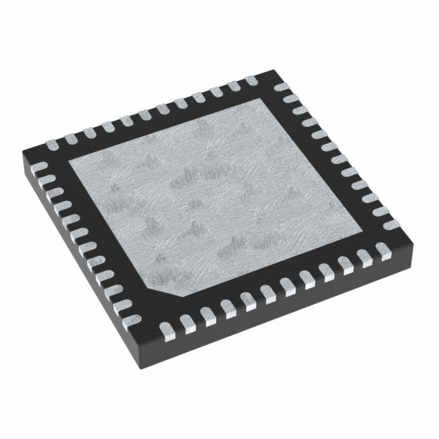
封装信息显示该器件采用56引脚TSSOP封装,并且有铅免费版本可供选择。
V385AGLF 价格&库存

很抱歉,暂时无法提供与“V385AGLF”相匹配的价格&库存,您可以联系我们找货

免费人工找货