New Features
Dual Supervisor
Batt Switch & Output
256K EEPROM
Dual Voltage Monitor with Integrated System Battery Switch and EEPROM
X45620
• Minimize EEPROM programming time
—64 byte page write mode
—Self-timed write cycle
—5ms write cycle time (typical)
• 400kHz 2-wire Interface
• 2.7V to 5.5V power supply operation
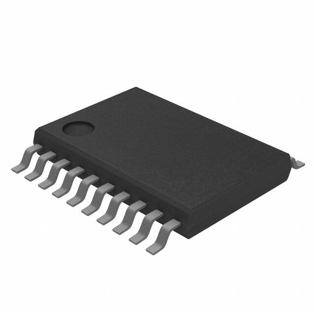
• Available package — 20-lead TSSOP
FEATURES
• Dual voltage monitoring
• Active low reset outputs
• Two standard reset threshold voltages
—Factory programmable threshold
• Lowline Output — zero delayed POR
• Reset signal valid to VCC = 1V
• System battery switch-over circuitry
• Selectable watchdog timer
—(0.15s, 0.4s, 0.8s, off)
• 256Kbits of EEPROM
• Built-in inadvertent write protection
—Power-up/power-down protection circuitry
—Protect 0, 1/4, 1/2 or all of EEPROM array with
programmable Block Lock™ protection
—In circuit programmable ROM mode
DESCRIPTION
The Xicor X45620 combines power-on reset control,
battery switch circuit, watchdog timer, supply voltage
supervision, secondary voltage supervision, block lock
protect and serial EEPROM in one package. This combination lowers system cost, reduces board space
requirements, and increases reliability.
Applying power to the device activates the power on
reset circuit which holds RESET active for a period of
time. This allows the power supply and oscillator to
stabilize before the processor can execute code.
BLOCK DIAGRAM
VOUT
V2MON
V2FAIL
+
VTRIP2
-
V2 Monitor
Logic
WDO
Watchdog Transition
Detector
Watchdog
Timer Reset
WP
Protect Logic
Data
Register
SDA
SCL
S0
S1
Address-Decoder
Command
Decode, Test
& Control
Logic
Status
Register
EEPROM
Array
Device
Select
Logic
VCC
(V1MON)
REV 1.2.6 9/25/03
BATT-ON
512 X 512
(32K X 8 Bit)
RESET/MR
VOUT
VOUT
VBATT
Reset &
Watchdog
Timebase
+
System
Battery
Switch
VCC Monitor
Logic
VTRIP1
-
www.xicor.com
Power on,
Low Voltage
Reset
Generation
LOWLINE
1 of 24
�X45620
DESCRIPTION (Continued)
A system battery switch circuit compares VCC
(V1MON) with VBATT input and connects VOUT to
whichever is higher. This provides voltage to external
SRAM or other circuits in the event of main power failure. The X45620 can drive 50mA from VCC and 250µA
from VBATT. The device switches to VBATT when VCC
drops below the low VCC voltage threshold and VBATT
> VCC..
The Watchdog Timer provides an independent protection mechanism for microcontrollers. When the microcontroller fails to restart a timer within a selectable time
out interval, the device activates the WDO signal. The
user selects the interval from three preset values.
Once selected, the interval does not change, even
after cycling the power.
The device’s low VCC detection circuitry protects the
user’s system from low voltage conditions, resetting
the system when VCC (V1MON) falls below the minimum VCC trip point (VTRIP1). RESET is asserted until
VCC returns to proper operating level and stabilizes. A
second voltage monitor circuit tracks the unregulated
supply or monitors a second power supply voltage to
provide a power fail warning. Xicor’s unique circuits
allow the threshold for either voltage monitor to be
reprogrammed to meet special needs or to fine-tune
the threshold for applications requiring higher precision. (Contact factory for custom VTRIP options)
PIN CONFIGURATION
20-Pin TSSOP
S0
1
20
VCC (V1MON)
S1
2
19
WP
NC
3
18
NC
LOWLINE
4
17
BATT-ON
NC
5
16
VOUT
V2FAIL
6
15
VBATT
V2MON
7
14
SCL
RESET/MR
8
13
NC
WDO
9
12
NC
10
11
SDA
VSS
Ordering Information
VCC Range
VTRIP1 Range
VTRIP2 Range
Package
Operating
Temperature Range
Part Number
4.75–5.5V
4.5–4.75V
2.55–2.7V
20L TSSOP
0°C–70°C
X45620V20
-40°C–85°C
X45620V20I
0°C–70°C
X45620V20-2.7
-40°C–85°C
X45620V20I-2.7
2.7–5.5V
REV 1.2.6 9/25/03
2.55–2.7V
1.7–1.80V
20L TSSOP
www.xicor.com
2 of 24
�X45620
PIN DESCRIPTION
Pin
Name
1
S0
Device Select Input. This pin has an internal pull down resistor. (>10MΩ typical)
2
S1
Device Select Input. This pin has an internal pull down resistor. (>10MΩ typical)
3
NC
No internal connections
4
LOWLINE
5
NC
6
V2FAIL
V2 Voltage Fail Output. This open drain output goes LOW when V2MON is less than VTRIP2 and
goes HIGH when V2MON exceeds VTRIP2. There is no power up reset delay circuitry on this pin.
7
V2MON
V2 Voltage Monitor Input. When the V2MON input is less than the VTRIP2 voltage, V2FAIL goes
LOW. This input can monitor an unregulated power supply with an external resistor divider or can
monitor a second power supply with no external components. Connect V2MON to VSS or VCC
when not used.
8
RESET
/MR
Reset Output/Manual Reset Input. This is an Input/Output pin.
RESET Output. This is an active LOW, open drain output which goes active whenever VCC falls
below the minimum VCC sense level. When RESET is active communication to the device is interrupted. RESET remains active until VCC rises above the minimum VCC sense level for tPURST. RESET
also goes active on power up and remains active for tPURST after the power supply stabilizes.
MR Input. This is an active LOW debounced input. When MR is active, the RESET pins are asserted. When MR is released, the RESET remains asserted for tPURST, and then released.
9
WDO
10
VSS
Ground
11
SDA
Serial Data. SDA is a bidirectional pin used to transfer data into and out of the device. It is an open
drain output, requires the use of a pull-up resistor.
14
SCL
Serial Clock. The SCL input is used to clock all data into and out of the device.
12–13
NC
No internal connections
15
VBATT
Battery Supply Voltage. This input provides a backup supply in the event of a failure of the primary VCC voltage. The VBATT voltage typically provides the supply voltage necessary to maintain
the contents of SRAM and also powers the internal logic to “stay awake.” If unused, connect
VBATT to ground.
16
VOUT
Output Voltage.
VOUT = VCC if VCC > VTRIP1.
IF VCC < VTRIP1, then,
VOUT = VCC if VCC > VBATT+0.03
VOUT = VBATT if VCC < VBATT-0.03
Note: There is hysteresis around VBATT ± 0.03V point to avoid oscillation at or near the
switchover voltage. A capacitance of 0.1µF must be connected to Vout to ensure stability.
REV 1.2.6 9/25/03
Function
Low VCC Detect. This open drain output signal goes LOW when VCC < VTRIP1 and immediately
goes HIGH when VCC > VTRIP1.
No internal connections
Watchdog Output. WDO is an active low, open drain output which goes active whenever the
watchdog timer goes active. WDO remains active for 150ms, then returns to the inactive state.
www.xicor.com
3 of 24
�X45620
PIN DESCRIPTION (Continued)
Pin
Name
Function
17
BATT-ON
Battery On. This CMOS output goes HIGH when the VOUT switches to VBATT and goes LOW
when VOUT switches to VCC. It is used to drive a external P-channel FET when VCC = VOUT and
current requirements are greater than 50mA.
The purpose of this output is to drive an external FET to get higher operating currents when the
VCC supply is fully functional. In the event of a VCC failure, the battery voltage is applied to the
VOUT pin and the external transistor is turned off. In this “backup condition,” the battery only needs
to supply enough voltage and current to keep SRAM devices from losing their data-there is no
communication at this time.
18
NC
No Connect
19
WP
Write Protect. The WP pin works in conjunction with a nonvolatile WPEN bit to “lock” the setting
of the Watchdog Timer control and the memory write protect bits. This pin has an internal pull down
20
VCC
(V1MON)
resistor. (>10MΩ typical)
REV 1.2.6 9/25/03
Supply Voltage/V1 Voltage Monitor Input. When the V1MON input is less than the VTRIP1
voltage, RESET and LOWLINE go ACTIVE.
www.xicor.com
4 of 24
�X45620
ABSOLUTE MAXIMUM RATINGS
COMMENT
Temperature under bias ...................–65°C to +135°C
Storage temperature ........................–65°C to +150°C
Voltage on any pin with
respect to VSS ...................................... –1.0V to +6V
D.C. output current
(all output pins except VOUT) ............................ 5mA
D.C. output current VOUT .................................... 50mA
Lead temperature (soldering, 10 seconds).........300°C
Stresses above those listed under “Absolute Maximum
Ratings” may cause permanent damage to the device.
This is a stress rating only; functional operation of the
device (at these or any other conditions above those
listed in the operational sections of this specification) is
not implied. Exposure to absolute maximum rating conditions for extended periods may affect device reliability.
RECOMMENDED OPERATING CONDITIONS
Temperature
Min.
Max.
Device Option
Supply Voltage
Commercial
0°C
70°C
-2.7
2.7V-5.5V
Industrial
–40°C
+85°C
Blank
4.75V-5.5V
D.C. OPERATING CHARACTERISTICS
(Over recommended operating conditions unless otherwise specified)
Limits
Symbol
Parameter
ICC1
VCC Supply Current (Active)
(Excludes IOUT) Read Memory array
(Excludes IOUT) Write nonvolatile
Memory
ICC2
Min.
Typ.(6)
Max.
Unit
mA
SCL = 400kHz
VOUT, RESET,
LOWLINE = Open
Note 1
µA
SDA = VCC, Any Input =
VSS or VCC: VOUT,
RESET, LOWLINE =
Open, Note 2
1.5
3.0
VCC Supply Current (Passive)
(Excludes IOUT)
Test Conditions
50
VCC Current (Battery Backup Mode)
(Excludes IOUT)
1
µA
VBATT = 2.8V, VOUT,
RESET = Open, Note 4,
1
IBATT1
VBATT Current (Excludes IOUT)
1
µA
VOUT = VCC, Note 4
IBATT2
VBATT Current (Excludes IOUT)
(Battery Backup Mode)
µA
VOUT = VBATT,
VBATT = 2.8V
VOUT, RESET = Open,
Note 4
VOUT1
Output Voltage (VCC > VBATT + 0.03V
or VCC > VTRIP1
VCC – 0.05
VCC – 0.5
V
V
IOUT = -5mA
IOUT = -50mA
VOUT2
Output Voltage (VCC < VBATT + 0.03V
and VCC < VTRIP1) {Battery Backup}
VBATT – 0.2
V
IOUT = -250µA
VOLB
Output (BATT-ON) LOW Voltage
0.4
V
IOL = 3.0mA (5V)
IOL = 1.0mA (3V)
VBSH
Battery Switch Hysteresis
(VCC < VTRIP1)
30
-30
mV
mV
ICC3
REV 1.2.6 9/25/03
50
www.xicor.com
VCC – 0.02
VCC – 0.2
Power Up
Power Down, Note 4
5 of 24
�X45620
D.C. OPERATING CHARACTERISTICS (CONTINUED)
(Over recommended operating conditions unless otherwise specified)
Limits
Symbol
Parameter
Min.
Typ.(6)
Max.
Unit
Test Conditions
VTRIP1
VCC Reset Trip Point Voltage
4.5
2.55
4.62
2.62
4.75
2.7
V
X45620
X45620-2.7
VTRIP2
V2MON Reset Trip Point Voltage
2.55
1.7
2.62
1.75
2.7
1.8
V
X45620
X45620-2.7
VOLR
Output (RESET, LOWLINE, WDO,
V2FAIL) LOW Voltage
0.4
V
IOL = 3.0mA (5V)
IOL = 1.0mA (3V)
Two Wire Interface
VIL
Input (SDA, S0, S1, SCL, WP) LOW
Voltage
-0.5
VCC x 0.3
V
Note 3
VIH
Input (SDA, S0, S1, SCL, WP) HIGH
Voltage
VCC x 0.7
VCC + 0.5
V
Note 3
ILI
Input Leakage Current (SDA, S1, S0,
SCL, WP)
±10
µA
Output (SDA) LOW Voltage
0.4
V
VOLS
IOL = 3.0mA (5V)
IOL = 1.0mA (3V), Note
4
Notes: (1) The device enters the Active state after any start, and remains active until 9 clock cycles later if the Device Select Bits in the Slave
Address Byte are incorrect; 200ns after a stop ending a read operation; or tWC after a stop ending a write operation.
(2) The device goes into Standby: 200ns after any Stop, except those that initiate a high voltage write cycle; t WC after a stop that
initiates a high voltage cycle; or 9 clock cycles after any start that is not followed by the correct Device Select Bits in the Slave
Address Byte.
(3) VIL min. and VIH max. are for reference only and are not tested.
(4) This parameter is guaranteed by characterization.
CAPACITANCE TA = +25°C, f = 1MHz, VCC = 5V
Symbol
Test
Max.
Unit
Conditions
COUT
Output Capacitance (SDA, RESET, V2FAIL, LOWLINE, BATT-ON, WDO)
8
pF
VOUT = 0V,
Note 1, 4
Input Capacitance (SDA, SCL, S0, S1, WP)
6
pF
VIN = 0V,
Note 1, 4
CIN
REV 1.2.6 9/25/03
www.xicor.com
6 of 24
�X45620
EQUIVALENT A.C. LOAD CIRCUIT AT 5V VCC
VCC
A.C. TEST CONDITIONS
VCC
1.53KΩ
1.53KΩ
Input pulse levels
VCC x 0.1 to VCC x 0.9
Input rise and fall times
10ns
Input and output timing level
VCC x0.5
BATT-ON
SDA
RESET
V2FAIL
LOWLINE
WDO
30pF
30pF
4481Ω
A.C. CHARACTERISTICS (Over recommended operating conditions, unless otherwise specified)
Read & Write Cycle Limits
Symbol
fSCL
Parameter
Min.
SCL clock frequency
Max.
400
tIN
Pulse width suppression time at inputs
50
tAA
SCL LOW to SDA Data Out Valid
0.1
0.9
Test
Unit Conditions
kHz
ns
Note 4
µs
Note 4
tBUF
Time the bus must be free before a new transmission can start
1.3
µs
Note 4
tLOW
Clock LOW period
1.3
µs
Note 4
tHIGH
Clock HIGH period
0.6
µs
Note 4
tSU:STA
Start condition setup time
0.6
µs
tHD:STA
Start condition hold time
0.6
µs
tSU:DAT
Data in setup time
100
ns
Note 4
tHD:DAT
Data in hold time
0
µs
Note 4
tSU:STO
Stop condition setup time
0.6
µs
Note 4
Data output hold time
50
ns
Note 4
tDH
Serial Output Timing
Min.
Max.
Unit
Test
Conditions
tR
SDA and SCL rise time
20 + .1Cb
300
ns
Note 4
tF
SDA and SCL fall time
20 + .1Cb
300
ns
Note 4
Symbol
Parameter
tSU:S0, S1, WP
S0, S1, and WP Setup Time
0.6
ns
Note 4
tHD:S0, S1, WP
S0, S1, and WP Hold Time
0
ns
Note 4
pF
Note 4, 7
Cb
REV 1.2.6 9/25/03
Capacitive load for each bus line
400
www.xicor.com
7 of 24
�X45620
POWER-UP TIMING(5)
Symbol
Parameter
Max.
Unit
Test Conditions
tPUR
Power-up to Read Operation
1
ms
Note 4
tPUW
Power-up to Write Operation
5
ms
Note 4
Notes: (5) tPUR and tPUW are the delays required from the time VCC is stable until the specified operation can be initiated. These parameters
are not 100% tested.
(6) Typical values are for TA = 25°C and nominal supply voltage (5V)
(7) Cb = total capacitance of one bus line in pF.
Bus Timing
tF
tHIGH
tHD:STA
tHD:DAT
tLOW
tR
SCL
tSU:STA
tSU:DAT
t SU:STO
SDA IN
tAA
tDH
tBUF
SDA OUT
S0, S1, and WP Pin Timing
SCL
Clk 1
Clk 9
Slave Address Byte
SDA IN
tSU: S0, S1, WP
tHD: S0, S1, WP
S0, S1 and WP
Write Cycle Limits
Symbol
(8)
TWC
Parameter
Min.
Typ.(6)
Max.
Unit
Test Conditions
Write Cycle Time
—
5
10
ms
Note 4
Notes: (8) tWC is the minimum cycle time to be allowed from the system perspective unless polling techniques are used. It is the maximum
time the device requires to automatically complete the internal write operation.
The write cycle time is the time from a valid stop condition of a write sequence to the end of the internal erase/write
cycle. During the write cycle, the X45620 bus interface circuits are disabled, SDA is allowed to remain HIGH, and
the device does not respond to its slave address.
REV 1.2.6 9/25/03
www.xicor.com
8 of 24
�X45620
Write Cycle Timing
SCL
8th Bit
SDA
ACK
Word n
tWC
Stop
Condition
Start
Condition
Power-Up and Power-Down Timing
VTRIP1
VBATT
VCC
0V
tPURST
tPURST
tRPD
RESET
VCC
VBAT
VOUT
0V
tVB1
tVB2
VOUT
BATT-ON
REV 1.2.6 9/25/03
www.xicor.com
9 of 24
�X45620
VCC to LOWLINE Timings
VTRIP1
VCC
VTRIP
tRPD
tF
0V
tR
VOH
LOWLINE
tRPD
VOL
VTRIP1
VBATT
0V
V2MON to V2FAIL Timings
VTRIP2
V2MON
0V
tRPD2
tRPD2
tF
tR
V2FAIL
RESET Output Timing
Symbol
tPURST
Parameter
RESET Time Out Period
PUP = 0
PUP = 1
Min.
Typ.(6)
Max.
Unit
75
400
150
600
250
800
ms
Test Conditions
Note 4
tRPD
VTRIP1 to RESET (Power down only), VTRIP1 to
LOWLINE
10
20
µs
Note 4
tRPD2
VTRIP2 to V2FAIL
10
20
µs
Note 4
200
300
ns
Note 4
tLR
LOWLINE to RESET delay (Power down only)
100
tF
VCC/V2MON Fall Time
1000
µs
Note 4, 9
tR
VCC/V2MON Rise Time
1000
µs
Note 4, 9
1
V
VRVALID
Reset Valid VCC
tVB1
VBATT + 0.03 V to BATT-ON (logical 0)
20
µs
Note 4
tVB2
VBATT – 0.03 V to BATT-ON (logical 1)
20
µs
Note 4
Notes: (9) This measurement is from 10% to 90% of the supply voltage.
REV 1.2.6 9/25/03
www.xicor.com
10 of 24
�X45620
WDT Restart Timing
SCL
tHD:STA
SDA
tWDO
VTRIP1. It switches to the battery backup mode
when VCC goes away.
Condition
Mode of Operation
VCC > VTRIP1
Normal Operation.
VCC > VTRIP1 &
VBATT = 0
Normal Operation without battery
back up capability.
0 ≤ VCC < VTRIP1
and VCC < VBATT
Battery Backup Mode; RESET
signal is asserted. No communication to the device is allowed.
Manual Reset
By connecting a push-button from MR to ground or driven
by logic, the designer adds manual system reset capability. The RESET pins is asserted when the push-button is
closed and remain asserted for tPURST after the pushbutton is released. This pin is debounced so a push-button connected directly to the device will have both clean
falling and rising edges on MR.
Figure 2. Example System Connection
Dual P-channel FET
Examples: IRF 7756, FDS9733A
Unregulated
Supply
5V
Reg
VCC
BATT-ON
SRAM
VOUT
VBATT
Address
Decode
V2MON
+
V2FAIL
Supercap
Enable
NMI
V2MON
Provides
Early Detection
of Power Failure
RESET
SDA, SCL
Addr
VCC
RESET
2-Wire µC
VSS
REV 1.2.6 9/25/03
www.xicor.com
13 of 24
�X45620
TWO WIRE SERIAL MEMORY
Device Select (S0, S1)
The memory portion of the device is a CMOS Serial
EEPROM array with Xicor’s block lock protection. The
array is internally organized as x 8. The device features
two wire and software protocol allowing operation on a
simple four-wire bus.
The device select inputs (S0, S1) are used to set bits in
the slave address. This allows up to four devices to
share a common bus. These inputs can be static or
actively driven. If used statically they must be tied to
VSS or VCC as appropriate. If actively driven, they must
be driven with CMOS levels (driven to VCC or VSS) and
they must be constant between each start and stop
issued on the SDA bus. These pins have an active pull
down internally and will be sensed as low if the pin is
left unconnected.
Two device select inputs (S0–S1) allow up to four
devices to share a common two wire bus.
A Control Register at the highest address location,
FFFFh, provides three write protection features: Software
Write Protect, Block Lock Protect, and Programmable
ROM. The Software Write Protect feature prevents any
nonvolatile writes to the device until the WEL bit in the
Control Register is set. The Block Lock Protection feature gives the user eight array block protect options,
set by programming three bits in the Control Register.
The Programmable ROM feature allows the user to
install the device with WP tied to VCC, write to and
Block Lock the desired portions of the memory array in
circuit, and then enable the In Circuit Programmable
ROM Mode by programming the WPEN bit HIGH in the
Control Register. After this, the Block Locked portions
of the array, including the Control Register itself, are protected from being erased if WP is high.
Xicor EEPROMs are designed and tested for applications requiring extended endurance. Inherent data
retention is greater than 100 years.
DETAILED PIN DESCRIPTIONS
Serial Clock (SCL)
The SCL input is used to clock all data into and out of
the device.
Serial Data (SDA)
SDA is a bidirectional pin used to transfer data into and
out of the device. It is an open drain output and may be
wire-ORed with any number of open drain or open collector outputs.
An open drain output requires the use of a pull-up
resistor. For selecting typical values, refer to the Pullup resistor selection graph at the end of this data
sheet.
REV 1.2.6 9/25/03
Write Protect (WP)
WP must be constant between each start and stop
issued on the SDA bus and is always active (not
gated). The WP pin has an active pull down to disable
the write protection when the input is left floating. The
Write Protect input controls the Hardware Write Protect
feature. When held LOW, Hardware Write Protection is
disabled. When this input is held HIGH, and the WPEN
bit in the Control Register is set HIGH, the Control
Register is protected, preventing changes to the Block
Lock Protection and WPEN bits.
DEVICE OPERATION
The device supports a bidirectional bus oriented protocol. The protocol defines any device that sends data
onto the bus as a transmitter, and the receiving device
as the receiver. The device controlling the transfer is a
master and the device being controlled is the slave.
The master will always initiate data transfers, and provide the clock for both transmit and receive operations.
Therefore, the device will be considered a slave in all
applications.
Clock and Data Conventions
Data states on the SDA line can change only during
SCL LOW. SDA state changes during SCL HIGH are
reserved for indicating start and stop conditions. Refer
to Figures 7 and 8.
Start Condition
All commands are preceded by the start condition,
which is a HIGH to LOW transition of SDA when SCL is
HIGH. The device continuously monitors the SDA and
SCL lines for the start condition and will not respond to
any command until this condition has been met.
www.xicor.com
14 of 24
�X45620
Figure 7. Data Validity
SCL
SDA
Data Stable
Data
Change
Figure 8. Definition of Start and Stop
SCL
SDA
Start Bit
Stop Bit
Stop Condition
All communications must be terminated by a stop condition, which is a LOW to HIGH transition of SDA when
SCL is HIGH. The stop condition is also used to place
the device into the standby power mode after a read
sequence. A stop condition can only be issued after
the transmitting device has released the bus.
Acknowledge
Acknowledge is a software convention used to indicate
successful data transfer. The transmitting device, either
master or slave, will release the bus after transmitting
eight bits. During the ninth clock cycle the receiver will
pull the SDA line LOW to acknowledge that it received
the eight bits of data. Refer to Figure 9.
In the read mode the device will transmit eight bits of
data, release the SDA line and monitor the line for an
acknowledge. If an acknowledge is detected and no
stop condition is generated by the master, the device
will continue to transmit data. If an acknowledge is not
detected, the device will terminate further data transmissions. The master must then issue a stop condition
to return the device to the standby power mode and
place the device into a known state.
The device will respond with an acknowledge after recognition of a start condition and its slave address. If
both the device and a write operation have been
selected, the device will respond with an acknowledge
after the receipt of each subsequent 8-bit word.
REV 1.2.6 9/25/03
www.xicor.com
15 of 24
�X45620
Figure 9. Acknowledge Response From Receiver
SCL from
Master
1
8
9
Data Output
from Transmitter
Data Output
fromReceiver
Start
Acknowledge
DEVICE ADDRESSING
WRITE OPERATIONS
Following a start condition, the master must output the
address of the slave it is accessing. The first four bits of
the Slave Address Byte are the device type identifier
bits. These must equal “1010”. The next 3 bits are the
device select bits “0”, S1, and S0. This allows up to 4
devices to share a single bus. These bits are compared
to the S0, S1, device select input pins. The last bit of
the Slave Address Byte defines the operation to be
performed. When the R/W bit is a one, then a read
operation is selected. When it is zero then a write operation is selected. Refer to Figure 10. After loading the
Slave Address Byte from the SDA bus, the device compares the device type bits with the value “1010” and the
device select bits with the status of the device select
input pins. If the compare is not successful, no
acknowledge is output during the ninth clock cycle and
the device returns to the standby mode.
Byte Write
For a write operation, the device follows “3 byte” protocol, consisting of one Slave Address Byte, one Word
Address Byte 1, and the Word Address Byte 0, which
gives the master access to any one of the words in the
array. Upon receipt of the Word Address Byte 0, the
device responds with an acknowledge, and waits for
the first eight bits of data. After receiving the 8 bits of
the data byte, the device again responds with an
acknowledge. The master then terminates the transfer
by generating a stop condition, at which time the
device begins the internal write cycle to the nonvolatile
memory. While the internal write cycle is in progress
the device inputs are disabled and the device will not
respond to any requests from the master. The SDA pin
is at high impedance. See Figure 11. Refer to bus timing on page 21.
On power up the internal address is undefined, so the
first read or write operation must supply an address.
The word address is either supplied by the master or
obtained from an internal counter, depending on the
operation. The master must supply the initial two Word
Address Bytes as shown in Figure 10.
The internal organization of the E2 array is 512 pages
by 64 bytes per page. The page address is partially
contained in the Word Address Byte 1 and partially in
bits 7 through 6 of the Word Address Byte 0. The byte
address is contained in bits 5 through 0 of the Word
Address Byte 0. See Figure 10.
REV 1.2.6 9/25/03
www.xicor.com
16 of 24
�X45620
Figure 10. Device Addressing
Device Type
Identifier
1
0
1
When the counter reaches the end of the page, it “rolls
over” and goes back to the first byte of the current
page. This means that the master can write 64-bytes to
the page beginning at any byte. If the master begins
writing at byte 32, and loads 64-bytes, then the first
32-bytes are written to bytes 32 through 63, and the
last 16 words are written to bytes 0 through 31. Afterwards, the address counter would point to byte 32. If the
master writes more than 64 bytes, then the previously
loaded data is overwritten by the new data, one byte at
a time.
Device
Select
0
0
S1
S0
R/W
Slave Address Byte
High Order Word Address
*
A14 A13 A12
A11 A10
A9
The master terminates the data byte loading by issuing
a stop condition, which causes the device to begin the
nonvolatile write cycle. As with the byte write operation,
all inputs are disabled until completion of the internal
write cycle. Refer to Figure 12 for the address,
acknowledge, and data transfer sequence.
A8
X45620 Word Address Byte 1
*This bit is 0 for access to the array and
1 for access to the Control Register
Low Order Word Address
A7
A6
A5
A4
A3
A2
A1
A0
D1
D0
Stop and Write Modes
Stop conditions that terminate write operations must
be sent by the master after sending at least 1 full data
byte and it’s associated ACK signal. If a stop is issued
in the middle of a data byte, or before 1 full data byte +
ACK is sent, then the device will reset itself without
performing the write. The contents of the array will not
be affected.
Word Address Byte 0
D7
D6
D5
D4
D3
D2
Data Byte
Page Write
The device is capable of a 64 byte page write operation.
It is initiated in the same manner as the byte write
operation; but instead of terminating the write operation
after the first data word is transferred, the master can
transmit up to sixty-three more words. The device will
respond with an acknowledge after the receipt of each
word, and then the byte address is internally incremented by one. The page address remains constant.
Acknowledge Polling
The maximum write cycle time can be significantly
reduced using Acknowledge Polling. To initiate
Acknowledge Polling, the master issues a start condition followed by the Slave Address Byte for a write or
read operation. If the device is still busy with the internal write cycle, then no ACK will be returned. If the
device has completed the internal write operation, an
ACK will be returned and the host can then proceed
with the read or write operation. Refer to Figure 13.
Figure 11. Byte Write Sequence
Signals from
the Master
SDA Bus
Signals from
the Slave
REV 1.2.6 9/25/03
S
T
A
R
T
Word Address
Byte 1
Slave
Address
Word Address
Byte 0
S
T
O
P
Data
S 1 0 1 0 0 S1S0 0
P
A
C
K
A
C
K
www.xicor.com
A
C
K
A
C
K
17 of 24
�X45620
Figure 12. Page Write Sequence
(0 ≤ n ≤ 64)
S
T
A
R
T
Signals from
the Master
Data
(0)
Word Address
Byte 0
Word Address
Byte 1
Slave
Address
Data
(n)
S
T
O
P
S 1 0 1 0 0 S1S0 0
SDA Bus
P
A
C
K
Signals from
the Slave
A
C
K
Figure 13. Acknowledge Polling Sequence
Issue
Start
Issue Slave
Address Byte
(Read or Write)
Issue Stop
NO
NO
YES
Continue Normal
Read or Write
Command Sequence?
A
C
K
READ OPERATIONS
Current Address Read
Internally, the device contains an address counter that
maintains the address of the last word read or written
incremented by one. After a read operation from the
last address in the array, the counter will “roll over” to
the first address in the array. After a write operation to
the last address in a given page, the counter will “roll
over” to the first address on the same page.
Upon receipt of the Slave Address Byte with the R/W bit
set to one, the device issues an acknowledge and then
transmits the eight bits of the Data Byte. The master terminates the read operation when it does not respond
with an acknowledge during the ninth clock and then
issues a stop condition. Refer to Figure 14 for the
address, acknowledge, and data transfer sequence.
YES
High
Voltage
Cycle Complete.
Continue
Sequence?
A
C
K
Read operations are initiated in the same manner as
write operations with the exception that the R/W bit of
the Slave Address Byte is set to one. There are three
basic read operations: Current Address Reads, Random Reads, and Sequential Reads. Refer to bus timing
on page 21.
Byte Load Completed
by Issuing Stop.
Enter ACK Polling
ACK
Returned?
A
C
K
Issue Stop
It should be noted that the ninth clock cycle of the read
operation is not a “don’t care.” To terminate a read
operation, the master must either issue a stop condition during the ninth cycle or hold SDA HIGH during
the ninth clock cycle and then issue a stop condition.
Note: After a power up sequence, the first read cannot
be a current address read.
PROCEED
REV 1.2.6 9/25/03
www.xicor.com
18 of 24
�X45620
The device will perform a similar operation called “Set
Current Address” if a stop is issued instead of the second start shown in Figure 15. The device will go into
standby mode after the stop and all bus activity will be
ignored until a start is detected. The effect of this operation is that the new address is loaded into the address
counter, but no data is output by the device.
Figure 14. Current Address Read Sequence
S
T
A
R
T
Signals from
the Master
SDA Bus
S
T
O
P
Slave
Address
S 1 0 1 0 0 S1S0 1
P
A
C
K
Signals from
the Slave
The next Current Address Read operation will read
from the newly loaded address.
Data
Random Read
Random read operation allows the master to access
any memory location in the array. Prior to issuing the
Slave Address Byte with the R/W bit set to one, the
master must first perform a “Dummy” write operation.
The master issues the start condition and the Slave
Address Byte with the R/W bit low, receives an
acknowledge, then issues the Word Address Byte 1,
receives another acknowledge, then issues the Word
Address Byte 0. After the device acknowledges receipt
of the Word Address Byte 0, the master issues another
start condition and the Slave Address Byte with the R/W
bit set to one. This is followed by an acknowledge and
then eight bits of data from the device. The master terminates the read operation by not responding with an
acknowledge and then issuing a stop condition. Refer
to Figure 9 for the address, acknowledge, and data
transfer sequence.
Sequential Read
Sequential reads can be initiated as either a current
address read or random read. The first Data Byte is
transmitted as with the other modes; however, the
master now responds with an acknowledge, indicating
it requires additional data. The device continues to output data for each acknowledge received. The master terminates the read operation by not responding with an
acknowledge and then issuing a stop condition.
The data output is sequential, with the data from
address n followed by the data from address n + 1. The
address counter for read operations increments
through all byte addresses, allowing the entire memory
contents to be read during one operation. At the end of
the address space the counter “rolls over” to address
0000h and the device continues to output data for each
acknowledge received. Refer to Figure 16 for the
acknowledge and data transfer sequence.
Figure 15. Random Read Sequence
Signals from
the Master
SDA Bus
S
T
A
R
T
Word Address
Byte 1
Slave
Address
S
T
A
R
T
Word Address
Byte 0
S 1 0 1 0 0 S1S0 0
1
S
A
C
K
Signals from
the Slave
S
T
O
P
Slave
Address
A
C
K
A
C
K
P
A
C
K
Data
Figure 16. Sequential Read Sequence
Signals from
the Master
SDA Bus
Signals from
the Slave
A
C
K
Slave
Address
S
A
C
K
S
T
O
P
A
C
K
S1S0 1
P
A
C
K
Data
(1)
Data
(2)
Data
(n–1)
Data
(n)
(n is any integer greater than 1)
REV 1.2.6 9/25/03
www.xicor.com
19 of 24
�X45620
CONTROL REGISTER (CR)
The Control Register is located in an area logically
separated from the array and is only accessible via a
byte write to the register address of FFFFH. The Control Register is physically part of the array.
The CR can only be modified by performing a byte write
operation directly to the address of the register and only
one data byte is allowed for each register write operation.
Prior to initiating a nonvolatile write to the CR, the WEL
and RWEL bits must be set using a two step process,
with the whole sequence requiring 3 steps.
The user must issue a stop, after sending this byte to
the register, to initiate the high voltage cycle that writes
PUP, WD1, WD0, BP1, BP0 and WPEN to the nonvolatile bits. The part will not acknowledge any data bytes
written after the first byte is entered. A stop must also
be issued after a volatile register write operation to put
the device into Standby. After a write to the CR, the
address counter contents are undefined.
The state of the CR can be read by performing a random read at the address of the register at any time.
Only one byte is read by the register read operation.
The part will reset itself after the first byte is read. The
master should supply a stop condition to be consistent
with the bus protocol, but a stop is not required to end
this operation. After the read of the CR, the address
counter contents are reset to zero, but the user will be
told these bits are undefined and instructed to do a
random read.
the WEL bit and zeros to the other bits of the control
register) or until the part powers up again. Writes to
WEL bit do not cause a high voltage write cycle, so the
device is ready for the next operation immediately after
the stop condition.
BP1, BP0: Block Protect Bits (Nonvolatile)
The Block Protect Bits, BP1 and BP0, determine which
blocks of the array are write protected. A write to a protected block of memory is ignored. The block protect
bits will prevent write operations to one of four segments of the array. The partitions are described in
Table 2.
WD1, WD0: Watchdog Timer Bits (Nonvolatile)
The Watchdog Timer circuit monitors the microprocessor activity by monitoring the SCL and SDA
pins. In normal operation, the microprocessor must
periodically restart the Watchdog Timer to prevent
WDO from going active. The watchdog timer is
restarted on the first HIGH to LOW transition on SCL
after a start command. The state of two nonvolatile
control bits in the Status Register determines the
watchdog timer period. The microprocessor can
change these watchdog bits by writing to the status
register.
The Watchdog Timer oscillator stops when in battery
backup mode. It re-starts when VCC returns.
Status Register Bit
WD1
WD0
Watchdog Time Out
(Typical)
0
0
800 milliseconds
0
1
400 milliseconds
1
0
150 milliseconds
1
1
Disabled (factory setting)
Table 1. Control Register
7
6
WPEN WD1
5
4
3
2
1
0
WD0 BP1 BP0 RWEL WEL PUP
RWEL: Register Write Enable Latch (Volatile)
The RWEL bit must be set to “1” prior to a write to Control Register.
WEL: Write Enable Latch (Volatile)
The WEL bit controls the access to the memory and to
the Register during a write operation. This bit is a volatile latch that powers up in the LOW (disabled) state.
While the WEL bit is LOW, writes to any address,
including any control registers will be ignored (no
acknowledge will be issued after the Data Byte). The
WEL bit is set by writing a “1” to the WEL bit and zeros
to the other bits of the control register. Once set, WEL
remains set until either it is reset to 0 (by writing a “0” to
REV 1.2.6 9/25/03
www.xicor.com
20 of 24
�X45620
Table 2. Block Protect Bits
BP1
BP0
Protected Addresses
Array Lock
0
0
None
None (factory setting)
0
1
6000h - 7FFFh (8K bytes)
Upper 1/4 (Q4)
1
0
4000h - 7FFFh (16K bytes)
Upper 1/2 (Q3, Q4)
1
1
0000h - 7FFFh (32K bytes)
Full Array (All)
Write Protect Enable Bit—WPEN (Nonvolatile)
The Write Protect (WP) pin and the Write Protect
Enable (WPEN) bit in the Control Register control the
Programmable Hardware Write Protect feature. Hardware Write Protection is enabled when the WP pin is
connected to VCC and the WPEN bit is HIGH, and disabled when WP pin is connected to ground. When the
chip is in ROM mode, nonvolatile writes are disabled to
all non-volatile bits in the CR, including the Block Protect bits and the WPEN bit itself, as well as to the block
protected sections in the memory array. Only the sections of the memory array that are not block protected
can be written. Note that since the WPEN bit is write
protected, it cannot be changed back to a LOW state;
so write protection is enabled as long as the WP pin is
held connected to VCC.
PUP: Power On Reset (Nonvolatile)
The Power on reset time (tPURST) bit, PUP, sets the
initial power on reset time. There are two standard
settings.
PUP
Time
0
150 ms (factory settings)
1
800 ms
Note 1. Watchdog timer is shipped disabled.
2. The tPURST time is set to 150ms at the factory.
Any changes to the Control Register take effect,
following either the next command (read or write) or
cycling the power to the device.
The recommended procedure for changing the
Watchdog Timer settings is to do a WREN, followed by
a write status register command. Then execute a
software loop to read the status register until an ACK is
returned (ACK polling) complete the read operation. A
valid alternative is to do a WREN, followed by a write
status register command. Then wait 10ms and do a
read status command.
Table 3. Write Protect Enable Bit and WP Pin Function
WP
WPEN
Memory Array Not
Block Protected
Memory Array
Block Protected
Block Lock Bits
WPEN Bit
Protection
LOW
X
Writes OK
Writes Blocked
Writes OK
Writes OK
Software
HIGH
0
Writes OK
Writes Blocked
Writes OK
Writes OK
Software
HIGH
1
Writes OK
Writes Blocked
Writes Blocked
Writes Blocked
Hardware
REV 1.2.6 9/25/03
www.xicor.com
21 of 24
�X45620
Writing to the Control Register
Changing any of the nonvolatile bits of the control register requires the following steps:
– Write a 02H to the CR to set the Write Enable Latch
(WEL). This is a volatile operation, so there is no
delay after the write. (Operation preceeded by a start
and ended with a stop).
OPERATIONAL NOTES
The device powers-up in the following state:
– The device is in the low power standby state.
– A “Start Bit” is required to enter an active state to
receive an instruction.
– The Write Enable Latch (WEL) is reset.
– Write a 06H to the CR to set both the Register Write
Enable Latch (RWEL) and the WEL bit. This is also a
volatile cycle. The zeros in the data byte are
required. (Operation preceeded by a start and ended
with a stop).
– The RESET Signal is active for tPURST.
– Write a value to the CR that has all the control bits
set to the desired state, with the WEL bit set to ‘1’
and the RWEL bit set to ‘0’. This can be represented
as nqrs t01u in binary, where n is the WPEN bit and
qrstu are the WD1, WD0, BP1, BP0 and PUP bits.
(Operation preceeded by a start and ended with a
stop). Since this is nonvolatile write cycle it will take
up to 10ms to complete. The RWEL bit is reset by
this cycle and the sequence must be repeated to
change the nonvolatile bits again. If bit 2 is set to ‘1’
in this third step (nqrs t11u) then the RWEL bit
remains set and the WPEN, PUP, WD1, WD0, BP1
and BP0 bits remain unchanged.
– The WEL bit must be set before writing to the
memory array.
Data Protection
The following circuitry has been included to prevent
inadvertent writes:
– The WEL and RWEL bits must be set before writing
to the nonvolatile bits of the Control Register.
– A valid slave byte and two address bytes must be
sent to the device with a valid ACK between each
byte.
– A “Stop Bit” must be received following a multiple of 8
data bits and completion of the data ACK bit.
– During the time RESET is active communication to
the device are ignored.
– A read operation occurring between any of the previous operations will not interrupt the register write
operation.
– The RWEL bit cannot be reset without writing to the
nonvolatile control bits in the control register, power
cycling the device or attempting a write to a write
protected block.
– Changes made to the Control Register non-volatile
bits become effective upon the next read operation of
the control register. (Power cycling will also activate
changes to the control register).
– Changes made to volatile bits in the Register take
effect immediately following the last data bit.
To illustrate, a sequence of writes to the device consisting of [02H, 06H, 02H] will reset all of the nonvolatile
bits to 0 and clear the RWEL bit. A sequence of [02H,
06H, 06H] will leave the nonvolatile bits unchanged
and the RWEL bit remains set.
When resetting the WEL bit, the operation goes active
immediately following the last data bit. The device will,
therefore, not respond with an ACK after the reset WEL
command data byte.
REV 1.2.6 9/25/03
www.xicor.com
22 of 24
�X45620
PACKAGING INFORMATION
20-Lead Plastic, TSSOP, Package Type V
.025 (.65) BSC
.169 (4.3)
.252 (6.4) BSC
.177 (4.5)
.252 (6.4)
.300 (7.62)
.047 (1.20)
.0075 (.19)
.0118 (.30)
.002 (.05)
.006 (.15)
.010 (.25)
Gage Plane
0° - 8°
Seating Plane
.019 (.50)
.029 (.75)
Detail A (20X)
.031 (.80)
.041 (1.05)
See Detail “A”
NOTE: ALL DIMENSIONS IN INCHES (IN PARENTHESES IN MILLIMETERS)
REV 1.2.6 9/25/03
www.xicor.com
23 of 24
�X45620
LIMITED WARRANTY
©Xicor, Inc. 2003 Patents Pending
Devices sold by Xicor, Inc. are covered by the warranty and patent indemnification provisions appearing in its Terms of Sale only. Xicor, Inc. makes no warranty,
express, statutory, implied, or by description regarding the information set forth herein or regarding the freedom of the described devices from patent infringement.
Xicor, Inc. makes no warranty of merchantability or fitness for any purpose. Xicor, Inc. reserves the right to discontinue production and change specifications and prices
at any time and without notice.
Xicor, Inc. assumes no responsibility for the use of any circuitry other than circuitry embodied in a Xicor, Inc. product. No other circuits, patents, or licenses are implied.
TRADEMARK DISCLAIMER:
Xicor and the Xicor logo are registered trademarks of Xicor, Inc. AutoStore, Direct Write, Block Lock, SerialFlash, MPS, BiasLock and XDCP are also trademarks of
Xicor, Inc. All others belong to their respective owners.
U.S. PATENTS
Xicor products are covered by one or more of the following U.S. Patents: 4,326,134; 4,393,481; 4,404,475; 4,450,402; 4,486,769; 4,488,060; 4,520,461; 4,533,846;
4,599,706; 4,617,652; 4,668,932; 4,752,912; 4,829,482; 4,874,967; 4,883,976; 4,980,859; 5,012,132; 5,003,197; 5,023,694; 5,084,667; 5,153,880; 5,153,691;
5,161,137; 5,219,774; 5,270,927; 5,324,676; 5,434,396; 5,544,103; 5,587,573; 5,835,409; 5,977,585. Foreign patents and additional patents pending.
LIFE RELATED POLICY
In situations where semiconductor component failure may endanger life, system designers using this product should design the system with appropriate error detection
and correction, redundancy and back-up features to prevent such an occurrence.
Xicor’s products are not authorized for use in critical components in life support devices or systems.
1. Life support devices or systems are devices or systems which, (a) are intended for surgical implant into the body, or (b) support or sustain life, and whose failure to
perform, when properly used in accordance with instructions for use provided in the labeling, can be reasonably expected to result in a significant injury to the user.
2. A critical component is any component of a life support device or system whose failure to perform can be reasonably expected to cause the failure of the life
support device or system, or to affect its safety or effectiveness.
REV 1.2.6 9/25/03
www.xicor.com
Characteristics subject to change without notice.
24 of 24
�