DATASHEET
ZL2105
FN6851
Rev. 2.00
March 30, 2011
3A Integrated Digital DC-DC Converter
Description
Features
The ZL2105 is an innovative power conversion and
management IC that combines an integrated
synchronous step-down DC-DC converter with key
power management functions in a small package,
resulting in a flexible and integrated solution.
Zilker Labs Digital-DC™ technology enables
unparalleled power management integration while
delivering industry-leading performance in a tiny
footprint.
Power Conversion
The ZL2105 can provide an output voltage from
0.6 V to 5.5 V from an input voltage between 4.5 V
and 14 V. Internal 4.5 A low RDS(ON) synchronous
power MOSFETs enable the ZL2105 to deliver
continuous loads up to 3 A with high efficiency,
and an internal Schottky bootstrap diode further
reduces discrete component count. The ZL2105
also supports phase spreading for reduced system
capacitance.
Power Management
Power management features such as digital softstart delay and ramp, sequencing, tracking, and
margining can be configured by simple pinstrapping or through an on-chip serial port. The
ZL2105 uses standard PMBus™ protocol for
communicating with other devices to provide
intelligent system power management.
High efficiency
3 A continuous output current
Integrated MOSFET switches
4.5 V to 14 V input range
0.54 V to 5.5 V output range (with margin)
±1% output voltage accuracy
200 kHz to 2 MHz switching frequency
Supports phase spreading
Small footprint (6 x 6 mm QFN package)
Digital soft start/stop
Precision delay and ramp-up
Power good/enable
Voltage tracking, sequencing, and margining
Output voltage/current monitoring
Thermal monitor w/ shutdown
Non-volatile memory
I2C/SMBus™ communication bus
PMBus compatible
Applications
Telecom and storage equipment
Digital set-top box
Industrial supplies
12 V distributed power systems
Point of load converters
VDDP
VDDP
VDDS
VR
VRA
2V5
VDDL
5V
LDO
BST
PWM
Control
&
Drivers
Power
Mgmt
NVM
SW
SW
VOUT
VSEN
PGND
PGND
CP2
VDR
CP1
Chg
Pump
SMBus
SDA
SA
2.5V
LDO
SCL
CFG
MGN
TRK
UVLO
DLY
SS
V0
V1
PG
Temp
Sense
SALRT
EN
SYNC
XTEMP
VIN
Figure 1. Block Diagram
FN6851 Rev. 2.00
March 30, 2011
Page 1 of 36
�ZL2105
Table of Contents
1. Electrical Characteristics ............................................................................................................................................... 3
2. Pin Descriptions ............................................................................................................................................................ 6
3. Typical Application Circuit ........................................................................................................................................... 8
4. ZL2105 Overview ....................................................................................................................................................... 10
4.1 Digital-DC Architecture ........................................................................................................................................ 10
4.2 Power Conversion Overview ................................................................................................................................ 11
4.3 Power Management Overview .............................................................................................................................. 12
4.4 Multi-mode Pins .................................................................................................................................................... 12
5. Power Conversion Functional Description .................................................................................................................. 13
5.1 Internal Bias Regulators and Input Supply Connections ...................................................................................... 13
5.2 High-side Driver Boost Circuit ............................................................................................................................. 13
5.3 Low-side Driver Supply Options .......................................................................................................................... 13
5.4 Dual Input Supply Configuration .......................................................................................................................... 14
5.5 Output voltage Selection ....................................................................................................................................... 15
5.6 Start-up Procedure................................................................................................................................................. 15
5.7 Soft Start Delay and Ramp Times ......................................................................................................................... 16
5.8 Switching Frequency and PLL .............................................................................................................................. 17
5.9 Component Selection ............................................................................................................................................ 19
5.10 Current Sensing and Current Limit Threshold Selection .................................................................................... 22
5.11 Loop Compensation ............................................................................................................................................ 22
5.12 Non-linear Response (NLR) Settings.................................................................................................................. 23
5.13 Efficiency Optimized Drive Dead-time Control ................................................................................................. 24
6. Power Management Functional Description ............................................................................................................... 24
6.1 Input Undervoltage Lockout ................................................................................................................................. 24
6.2 Power Good (PG) and Output Overvoltage Protection ......................................................................................... 25
6.3 Output Overvoltage Protection ............................................................................................................................. 25
6.4 Output Pre-Bias Protection ................................................................................................................................... 25
6.5 Output Overcurrent Protection .............................................................................................................................. 26
6.6 Thermal Overload Protection ................................................................................................................................ 26
6.7 Voltage Tracking................................................................................................................................................... 27
6.8 Voltage Margining ................................................................................................................................................ 28
6.9 I2C/SMBus Communications ................................................................................................................................ 29
6.10 I2C/SMBus Device Address Selection ................................................................................................................ 29
6.11 Phase Spreading .................................................................................................................................................. 29
6.12 Output Sequencing .............................................................................................................................................. 30
6.13 Monitoring via I2C/SMBus ................................................................................................................................. 31
6.14 Temperature Monitoring using the XTEMP Pin ................................................................................................. 31
6.15 Non-Volatile Memory and Device Security Features ......................................................................................... 32
7. Package Dimensions.................................................................................................................................................... 33
8. Ordering Information .................................................................................................................................................. 34
9. Related Documentation ............................................................................................................................................... 34
10. Revision History ........................................................................................................................................................ 35
FN6851 Rev. 2.00
March 30, 2011
Page 2 of 36
�ZL2105
1. Electrical Characteristics
Table 1. Absolute Maximum Ratings
Voltage measured with respect to SGND. Operating beyond these limits may cause permanent damage to the device.
Functional operation beyond the Recommended Operating Conditions is not implied.
Parameter
DC Supply Voltage
Logic Supply Voltage
High Side Supply Voltage
High Side Boost Voltage
Switch Node Current
Internal Drive References
Internal 2.5 V Reference
Logic I/O Voltage
Pin
VDDP, VDDS, VDR
VDDL
BST
BST - SW
SW
VR, VRA
V25
EN, MGN, PG, SDA, SCL, SA,
SALRT, SS, DLY, SYNC,
VTRK, UVLO, V(0,1), ILIM,
VSEN, CFG
Ground Differential
Value
-0.3 to 17
-0.3 to 6.5
-0.3 to 25
-0.3 to 8
4.5
-0.3 to 6.5
-0.3 to 3
Unit
V
V
V
V
A
V
V
-0.3 to 6.5
V
DGND - SGND
PGND - SGND
±0.3
V
VR
30
mA
VRA
V25
–
150
60
-55 to 150
-55 to 150
300
mA
mA
°C
°C
°C
MOSFET Drive Reference
Current
Analog Reference Current
2.5 V Reference Current
Junction Temperature
Storage Temperature
Lead Temperature
Comments
Optional
Sink or Source
–
All
Soldering, 10 s
Table 2. Recommended Operating Conditions and Thermal Information
Symbol
Parameter
Min
Typ
Max
Unit
VDDS tied to VR, VRA
4.5
–
5.5
V
VR, VRA floating
5
–
14
V
VDDL (optional)
3.0
–
5.5
V
VDR
10
–
14
V
VOUT
0.54
–
5.5
V
Operating Junction Temperature Range
TJ
-40
–
125
°C
Junction to Ambient Thermal Impedance2
ΘJA
–
35
–
°C/W
ΘJC
–
5
–
°C/W
Input Supply Voltage Range, VDDP, VDDS
(See Figure 8)
Logic Supply Voltage Range, VDDL
Internal Driver Supply, VDR
Output Voltage Range
1
Junction to Case Thermal Impedance3
Notes:
1. Includes margin
2. ΘJA is measured in free air with the device mounted on a multi-layer FR4 test board and the exposed metal pad
soldered to a low impedance ground plane using multiple vias.
3. For ΘJC, the “case” temperature is measured at the center of the exposed metal pad. See Figure 4 for thermal
derating.
FN6851 Rev. 2.00
March 30, 2011
Page 3 of 36
�ZL2105
Table 3. Electrical Specifications
VDDP = VDDS = 12 V, TA = -40C to 85C unless otherwise noted. Typical values are at TA = 25C.
Min
(Note 3)
Typ
Max
(Note 3)
Unit
–
–
–
–
2
5
8
10
3
6
16
20
mA
mA
mA
mA
–
0.7
2
mA
–
225
500
µA
4.5
4.5
2.25
5.2
5.2
2.5
5.5
5.5
2.75
V
V
V
–
0.6
–
–
-1
–
7
0.007
–
10
0
–
–
–
10
±0.025
–
100
–
–
6
–
–
100
3
5.0
–
–
1
200
200
500
–
100
200
–
A
V
mV
% FS
%
µA
ms
s
ms
ms
ms
µs
IOL ≤ 4 mA
IOH ≥ -2 mA
-250
–
–
2.0
–
2.25
–
1.4
–
–
–
250
0.8
–
–
0.4
–
nA
V
V
V
V
V
VTRK = 5.5 V
100% Tracking, VOUT - VTRK
–
- 100
110
–
200
+ 100
µA
mV
Conditions
Parameter
Input and Supply Characteristics
IDDS supply current
IDDL supply current
IDDS shutdown current
IDDL shutdown current
VR reference output voltage
VRA reference output voltage
V25 reference output voltage
Output Characteristics
Output Current
Output voltage adjustment range1
Output voltage setpoint resolution
VSEN output voltage accuracy
VSEN input bias current
Soft start delay duration range2
fSW = 200 kHz, no load
fSW = 1 MHz, no load
fSW = 200 kHz, no load
fSW = 1 MHz, no load
EN = 0 V, VDDL tied to VRA,
No I2C/SMBus activity
EN = 0 V, VDDL = 5 V,
No I2C/SMBus activity
VDD > 5.5 V, IVR < 5 mA
VDD > 5.5 V, IVRA < 35 mA
IV25 < 50 mA
VIN > VOUT
Set using resistors
Set using I2C/SMBus
Includes line, load, temp
VSEN = 5.5 V
Set using DLY pin or resistor
Set using I2C/SMBus
Soft start delay duration accuracy
Soft start ramp duration range
Soft start ramp duration accuracy
Logic Input/Output Characteristics
Logic input current
Logic input low, VIL
Logic input OPEN (N/C)
Logic input high, VIH
Logic output low, VOL
Logic output high, VOH
Tracking
VTRK input bias current
VTRK tracking accuracy
Notes:
Set using SS pin
Set using resistor or via I2C
EN, SCL, SDA pins
Multi-mode logic pins
1. Does not include margin
2. The device requires approximately 6 ms following an enable signal and prior to output ramp. The minimum
settable delay is 7 ms.
3. Compliance to datasheet limits is assured by one or more methods: production test, characterization and/or design.
Table 3 is continued on the following page
FN6851 Rev. 2.00
March 30, 2011
Page 4 of 36
�ZL2105
Table 3. Electrical Characteristics (continued)
VDDP = VDDS = 12 V, TA = -40C to 85C unless otherwise noted. Typical values are at TA = 25C.
Parameter
Conditions
Oscillator and Switching Characteristics
Sourcing or Sinking
Switch node current, ISW
Switching frequency range
Predefined settings
Switching frequency set-point accuracy
Minimum SYNC pulse width
External clock source
Input clock frequency drift tolerance
Maximum duty cycle
ISW = 1 A, VGS = 4.7 V
RDS(ON) of High Side N-channel FETs
ISW=1A, VGS=8.5V, Charge Pump
RDS(ON) of Low Side N-channel FETs
ISW=1A, VGS=12V
Fault Protection Characteristics
UVLO threshold range
UVLO setpoint accuracy
Factory default
UVLO hysteresis
Configurable via I2C/SMBus
UVLO delay
Factory default
Power good low threshold
Factory default
Power good high threshold
Factory default
Power good hysteresis
Using pin-strap or resistor 1
Power good delay
Configurable via I2C/SMBus
Factory default
VSEN undervoltage threshold
Configurable via I2C/SMBus
Factory default
VSEN overvoltage threshold
Configurable via I2C/SMBus
VSEN undervoltage hysteresis
Factory default
VSEN undervoltage/ overvoltage fault
response time
Configurable via I2C/SMBus
Peak current limit threshold
Using ILIM pin or via I2C/SMBus
Current limit setpoint accuracy
Factory default
Current limit shutdown delay
Configurable via I2C/SMBus
Factory default
Thermal protection threshold (junction
temperature)
Configurable via I2C/SMBus
Thermal protection hysteresis
Notes:
Min
(Note 3)
Typ
Max
(Note 3)
Unit
–
200
-5
150
-13
90
–
–
–
3
–
–
–
–
–
125
123
114
4.0
2000
5
–
13
–
180
140
130
A
kHz
%
ns
%
%
mΩ
mΩ
mΩ
3.79
-2
–
0
–
–
–
–
0
0
–
0
–
0
–
–
5
0.2
–
–
1
–
-40
–
–
–
3
–
–
90
115
5
–
–
85
–
115
–
5
16
–
–
±100
5
–
125
–
15
13.2
2
–
100
2.5
–
–
–
200
500
–
110
–
115
–
–
60
4.5
–
–
32
–
125
–
V
%
%
%
µs
% VOUT
% VOUT
%
ms
s
% VOUT
% VOUT
% VOUT
% VOUT
% VO
µs
µs
A
mA
tSW 2
tSW 2
°C
°C
°C
1. Factory default Power Good delay is set to the same value as the soft start ramp time.
2. tSW = 1/fSW, where fSW is the switching frequency.
3. Compliance to datasheet limits is assured by one or more methods: production test, characterization and/or design.
FN6851 Rev. 2.00
March 30, 2011
Page 5 of 36
�ZL2105
28
29
30
31
32
33
34
1
27
2
26
3
25
4
24
ZL2105
5
23
6
22
7
Exposed Paddle
8
Connect to SGND
21
20
9
18
17
16
15
14
13
12
VR
BST
VDDP
VDDP
SW
SW
PGND
PGND
CP2
V0
V1
DLY
SS
VTRK
VSEN
NC
VDR
CP1
11
19
10
DGND
SYNC
SA
UVLO
ILIM
SCL
SDA
SALRT
XTEMP
35
36
PG
EN
CFG
MGN
FC
V25
VDDS
VDDL
VRA
2. Pin Descriptions
Figure 2. ZL2105 Pin Configurations (top view)
Table 4. Pin Descriptions
Pin
Label
Type1
1
DGND
PWR
2
SYNC
I/O, M
3
4
5
6
7
8
9
10,11
SA
UVLO
ILIM
SCL
SDA
SALRT
XTEMP
V0, V1
I,M
I,M
I,M
I/O
I/O
O
I
I,M
12
DLY
I,M
13
SS
I,M
Description
Digital ground. Common return for digital signals. Connect to low impedance ground
plane.
Clock synchronization input. Used to set switching frequency of internal clock or for
synchronization to external frequency reference. Programmable open drain output.
Factory default is push-pull
Serial address pin used to assign unique SMBus address to each IC.
Sets the input undervoltage lockout threshold that disables the device.
Sets the current limit threshold level.
Serial clock signal for system communications.
Serial data signal for system communications.
SMBus alert signal.
External temperature sensor input.
Output voltage select pins. Used to set the output voltage.
Soft start delay select pin. Sets the delay from when EN is asserted until the output
voltage starts to ramp.
Digital soft-start/stop. Sets the ramp period for the output to reach the desired regulation
point (after soft-start delay period, if applicable).
Track input. Allows the output to track another voltage.
Output voltage positive feedback sensing node.
No internal connection.
Supply pin for internal drivers.
Level-shift charge pump for 5 V operation. Connect external capacitor.
VTRK
I
14
VSEN
I
15
NC
16
VDR
PWR
17
CP1,CP2
I/O
18, 19
Notes:
1. I = Input, O = Output, PWR = Power or Ground. M = Multi-mode pins.
FN6851 Rev. 2.00
March 30, 2011
Page 6 of 36
�ZL2105
Table 4. Pin Descriptions (continued)
Pin
Label
Type1 Description
PGND
PWR
Power ground. Common return for internal switching MOSFETs.
20,21
SW
I/O
Switching node (level-shift common).
22,23
VDDP
PWR
Bias power for internal switching MOSFETs (return is PGND).
24,25
BST
PWR
Bootstrap VDD for level-shift driver (referenced to SW).
26
Regulated bias from internal 5V low-dropout regulator (return is PGND). Decouple
VR
PWR
with a 4.7 µF capacitor to PGND.
27
Connect 91Ω resistor between VR and VRA.
Regulated 5 V bias for internal analog circuitry (return is SGND).
VRA
PWR
Decouple with a 4.7 µF capacitor to SGND.
28
Connect 91Ω resistor between VR and VRA.
Internal logic supply. Connect to VRA or apply a 3.0-5.5 V external supply. Return is
VDDL
PWR
29
SGND.
VDDS
PWR
IC supply voltage (return is SGND).
30
Regulated bias from internal 2.5 V low-dropout regulator. Decouple with a 10µF
V25
PWR
31
capacitor.
FC
I
Frequency compensation select pin. Used to set loop compensation.
32
MGN
I
Signal that enables margining of output voltage.
33
CFG
I
Configuration pin. Sets switching phase delay and sequencing order.
34
EN
I
Enable input. Active high signal enables the device.
35
36
PG
O
ePad
SGND
PWR
Power good output. This pin transitions high 100 ms after output voltage stabilizes
within regulation band. Programmable open drain output. Factory default is open drain.
Exposed thermal pad. Common return for analog signals; internal connection to
SGND. Connect to low impedance ground plane.
Notes:
1. I = Input, O = Output, PWR = Power or Ground. M = Multi-mode pins. Please refer to Section 4.4 “Multi-mode Pins,” on
page 12.
FN6851 Rev. 2.00
March 30, 2011
Page 7 of 36
�ZL2105
3. Typical Application Circuit
The following application circuit represents a typical implementation of the ZL2105.
CDD
2.2µF
ENABLE
PGOOD
F.B.*
VIN
12V
CRA
4.7µF
28
29
31
30
32
34
33
35
CIN
100µF
RVR
91Ω
CR
4.7µF
CB
47nF
LOUT
4.7µH
VOUT
3.3V
COUT
150µF
18
ePAD
(SGND)
9
17
8
16
7
15
I C/SMBus
14
6
2
ZL2105
13
5
12
4
VR 27
BST 26
VDDP 25
VDDP 24
SW 23
SW 22
PGND 21
PGND 20
CP2 19
V0
V1
DLY
SS
VTRK
VSEN
NC
VDR
CP1
3
11
2
DGND
SYNC
SA
UVLO
ILIM
SCL
SDA
SALRT
XTEMP
10
1
PG
EN
CFG
MGN
FC
V25
VDDS
VDDL
VRA
36
C25
10µF
CDR
100nF
* Ferrite bead is optional for input noise suppression
Figure 3. 12 V to 3.3 V / 3 A Application Circuit
(10.8 V UVLO, 10 ms SS delay, 50 ms SS ramp, 12 V used for low-side FET driver)
FN6851 Rev. 2.00
March 30, 2011
Page 8 of 36
�ZL2105
For all applications, the ZL2105 must be derated according to the Safe Operating Area (SOA) curves.
Output Voltage, VOUT (V)
ZL2105 SOA vs Frequency
VIN = 12V
5
4
VIN = 5V
3
VIN = 4.5V
2
TJ ≤ 125°C
L = 2.2μH
1
Circuit from Figure 3 except L=2.2μH.
Appropriate L should be selected as described in Section 5.9 of data sheet
0.2
0.4
0.6
0.8
1.0
1.2
1.4
1.6
1.8
2.0
Switching Frequency, FSW (MHz)
Max Conversion Ratio vs Switching Frequency
VOUT / VIN
TJ < 125 C
0.95
0.9
0.85
0.8
0.75
0.7
0.65
0.6
0.55
0.5
0.45
0.4
0.35
0.3
VOUT may not exceed 5.5V at any time
0.2
0.3
0.4
0.5
0.6
0.7
0.8
0.9
1
1.1
1.2
1.3
1.4
1.5
1.6
1.7
1.8
1.9
2
f SW (MHz)
Figure 4. ZL2105 SOA Curves
FN6851 Rev. 2.00
March 30, 2011
Page 9 of 36
�ZL2105
4. ZL2105 Overview
4.1 Digital-DC Architecture
The ZL2105 is an innovative mixed-signal power
conversion and power management IC based on Zilker
Labs patented Digital-DC technology that provides an
integrated, high performance step-down converter for
point of load applications. The ZL2105 integrates all
necessary PWM control circuitry as well as
synchronous 4.5 A N-channel MOSFETs in order to
provide an extremely small solution for providing load
currents up to 3 A. Its unique PWM loop utilizes an
ideal mix of analog and digital blocks to enable precise
control of the entire power conversion process with no
software required, resulting in a very flexible device
that is also very easy to use. An extensive set of power
management functions are fully integrated and can be
configured using simple pin connections. The user
configuration can be saved in an internal non-volatile
memory (NVM). Additionally, all functions can be
configured and monitored via the SMBus hardware
interface using standard PMBus commands, allowing
ultimate flexibility.
Once enabled, the ZL2105 is immediately ready to
regulate power and perform power management tasks
with
no
programming
required.
Advanced
configuration options and real-time configuration
changes are available via the I2C/SMBus interface if
desired and continuous monitoring of multiple
operating parameters is possible with minimal
interaction from a host controller. Integrated subregulation circuitry enables single supply operation
from any supply between 4.5 V and 14 V with no
secondary bias supplies needed. The ZL2105
FN6851 Rev. 2.00
March 30, 2011
can also be configured to operate from a 3.3 V or 5 V
standby supply when the main power rail is not
present, allowing the user to configure and/or read
diagnostic information from the device when the main
power has been interrupted or is disabled.
The ZL2105 can be configured by simply connecting
its pins according to the tables provided in the
following sections. Additionally, a comprehensive set
of tools and application notes are available to help
simplify the design process. An evaluation board is
also available to help the user become familiar with the
device. This board can be evaluated as a standalone
platform using pin configuration settings. A
Windows™-based GUI is also provided to enable full
configuration and monitoring capability via the
I2C/SMBus interface using an available computer and
the included USB cable.
Application notes and reference designs are available
to assist the user in designing to specific application
demands. Please register for My ZL on
www.intersil.com/zilkerlabs/ to access the most up-todate documentation or call your local Zilker Labs sales
office to order an evaluation kit.
Page 10 of 36
�ZL2105
4.2 Power Conversion Overview
CFG V(0,1)
VDDP
SS
VDDS
MGN ILIM DLY
VR
EN
>
VRA
PG
VDDL
INPUT VOLTAGE BUS
>
BST
VTRK
NVM
POWER MANAGEMENT
DIGITAL
DIGITAL
COMPENSATOR
COMPENSATOR
FC
LDO
ISENSE
D-PWM
SW
NLR
SYNC
GEN
SYNC
VOUT
MOSFET
DRIVERS
PLL
ADC
-
VDR
+
ISENSE
ADC
RESET
REF
VR
VDD
CP1
CHG
PUMP
CP2
VSEN
SALRT
SDA
SCL
SA
ADC
COMMUNICATION
MUX
XTEMP
TEMP
SENSOR
Figure 5. ZL2105 Block Diagram
The ZL2105 operates as a voltage-mode, synchronous
buck converter with a selectable constant frequency
PWM control scheme. The ZL2105 incorporates dual
low RDS(ON) synchronous MOSFETs to help minimize
the required circuit footprint.
CIN
DB
LDO
CB
L1
VOUT
PWM
QL
COUT
ZL2105
Figure 6. Synchronous Buck Converter
Figure 6 illustrates the basic synchronous buck
converter topology showing the primary power train
components. This converter is also called a step-down
converter, as the output voltage must always be lower
than the input voltage. The ZL2105 integrates two
MOSFETs; QH is the top control MOSFET and QL is
the bottom synchronous MOSFET. The amount of time
that QH is on as a fraction of the total switching period
FN6851 Rev. 2.00
March 30, 2011
V
D OUT
V IN
During time D, QH is on and VIN – VOUT is applied
across the inductor.
VIN
QH
is known as the duty cycle D, which is described by the
following equation:
As shown in Figure 5, the output voltage is directly
applied to the VSEN pin. The VSEN signal is then
compared to an internal programmable reference
voltage that is set to the desired output voltage level.
The error signal derived from this comparison is
converted to a digital value with a fast analog to digital
(A/D) converter. The digital signal is also applied to an
adjustable digital compensation filter, and the
compensated signal is used to derive the appropriate
PWM duty cycle for driving the internal MOSFETs.
The ZL2105 also incorporates a non-linear response
(NLR) loop to improve the response time and reduce
the output deviation as a result of a load transient. The
ZL2105 monitors the power converter’s operating
conditions and continuously adjusts the turn-on and
turn-off timing of the high-side and low-side
MOSFETs to optimize the overall efficiency of the
power supply.
Page 11 of 36
�ZL2105
4.3 Power Management Overview
The ZL2105 incorporates a wide range of configurable
power management features that are simple to
implement with no external components. Additionally,
the ZL2105 includes circuit protection features that
continuously safeguard the device and load from
damage due to unexpected system faults. The ZL2105
can continuously monitor input voltage, output
voltage/current, internal temperature, and the
temperature of an external thermal diode. A Power
Good output signal is also included to enable power-on
reset functionality for an external processor.
All power management functions can be configured
using either pin configuration techniques (see Figure 7)
or via the I2C/SMBus interface. Monitoring parameters
can also be pre-configured to provide alerts for specific
conditions. See Application Note AN2013 for more
details on SMBus monitoring.
4.4 Multi-mode Pins
Most power management features can be configured
using the multi-mode pins. The multi-mode pins can
respond to four different connections as shown in
Table 5. These pins are sampled when power is applied
or by issuing a PMBus Restore command (See
Application Note AN2013).
Pin-strap Settings: Using this method, each pin can
take on one of three possible states: LOW, OPEN, or
HIGH. These pins can be connected to the VR or V25
pins for logic HIGH settings, as either pin provides a
regulated voltage higher than 2 V. Using a single pin
one of three settings can be selected, and using two
pins the user can select one of nine settings.
Logic
high
Open
ZL2105
ZL2105
Multi-mode Pin
Multi-mode Pin
RSET
Logic
low
Pin-strap
Settings
Resistor
Settings
Figure 7. Pin-strap and Resistor Setting Examples
Resistor Settings: This method allows a greater range
of adjustability when connecting a finite value resistor
(in a specified range) between the multi-mode pin and
SGND. Standard 1% resistor values are used, and only
every fourth E96 resistor value is used so the device
can reliably recognize the value of resistance
connected to the pin while eliminating the error
associated with the resistor accuracy. A total of 25
unique selections are available using a single resistor.
I2C/SMBus Method: Almost any ZL2105 function can
be configured via the I2C/SMBus interface using
standard PMBus commands. Additionally, any value
that has been configured using the pin-strap or resistor
setting methods can also be re-configured and/or
verified via the I2C/SMBus. See Application Note
AN2013 for more details.
The SMBus device address and VOUT_MAX are the
only parameters that must be set by external pins. All
other device parameters can be set via the I2C/SMBus.
The device address is set using the SA pin.
VOUT_MAX is determined as 10% greater than the
voltage set by the V0 and V1 pins.
Table 5. Multi-mode Pin Configuration
Pin Tied To
Value
LOW
< 0.8 VDC
(Logic LOW)
OPEN
No connection
(N/C)
HIGH
> 2.0 VDC
(Logic HIGH)
Resistor to SGND
FN6851 Rev. 2.00
March 30, 2011
Set by resistor value
Page 12 of 36
�ZL2105
5. Power Conversion Functional Description
5.1 Internal Bias Regulators and Input Supply
Connections
The ZL2105 employs three internal low dropout
(LDO) regulators to supply bias voltages for internal
circuitry as follows:
VR: The VR LDO provides a regulated 5 V bias
supply for the MOSFET driver circuits. It is powered
from the VDDS pin. A 4.7 µF filter capacitor is
required at the VR pin.
VRA: The VRA LDO provides a regulated 5 V bias
supply for the current sense circuit and other analog
circuitry. It is powered from the VDDS pin. A small
filter capacitor is required at the VRA pin. For single
supply operation, this pin should be connected to the
VDDL pin so the VRA LDO can be used to power the
digital core logic circuitry.
V25: The V25 LDO provides a regulated 2.5 V bias
supply for the main controller circuitry. It is powered
from the VDDL pin. A 10 µF filter capacitor is
required at the V25 pin.
When the input supply (VDDS) is higher than 5.5 V,
the VR and VRA pins should not be connected to any
other pins. They should have a filter capacitor and a
91Ω resistor attached as shown in Figure 8. Due to the
dropout voltage associated with the VR and VRA bias
regulators, the VDDS pin must be connected to the VR
and VRA pins for designs operating from a supply
below 5.5 V. Figure 8 illustrates the required
connections for both cases.
The gate drive voltage for the high-side MOSFET
driver is generated by a floating bootstrap capacitor, CB
(see Figure 6). When the lower MOSFET (QL) is
turned on, the SW node is pulled to ground and the
capacitor is charged from the internal VR bias
regulator through diode DB. When QL turns off and the
upper MOSFET (QH) turns on, the SW node is pulled
up to VDDP and the voltage on the bootstrap capacitor is
boosted approximately 5V above VDDP to provide the
necessary voltage to power the high-side driver. An
internal Schottky diode is used with CB to help
maximize the high-side drive supply voltage.
5.3 Low-side Driver Supply Options
The ZL2105 provides multiple options for powering
the internal low-side MOSFET drivers as follows:
12 V Supply: When operating from a 12 V input supply
(or any supply 9 V or higher), efficiency can be
optimized by operating the low-side MOSFET driver
directly from the input supply. Connecting the input
supply to the VDR pin (with no external capacitor
connected between CP1 and CP2) applies the input
supply directly to the low-side driver. This is the
simplest method of powering the low-side driver and
requires the fewest components. Figure 9 illustrates the
required connections for implementing this
configuration.
12V
VIN
ZL2105
VRA
VDDS
VR
ZL2105
91Ω
VRA
VRA
VR
VDDL
VDDS
VDDS
VIN
5.2 High-side Driver Boost Circuit
VR
BST
4.5V ≤ VIN ≤ 5.5V
5.5V < VIN ≤ 14V
VDDP
VDDP
SW
VOUT
SW
PGND
PGND
CP1
CP2
VDR
Note: the internal bias regulators, VR and VRA, are
not designed to be outputs for powering other circuitry.
Do not attach external loads to either of these pins. The
multi-mode pins may be connected to the V25 pin for
logic HIGH settings.
ZL2105
SGND
Figure 8. Input Supply Connections
12V
Figure 9. Using an External 12 V Supply to Power
the Low-side Driver
FN6851 Rev. 2.00
March 30, 2011
Page 13 of 36
�ZL2105
VRA
VDDL
5V
VDDS
Internal Charge Pump: A voltage doubler circuit can
be used to optimize efficiency when operating from an
input supply that is below 9 V or may occasionally
drop below 9 V. The internal charge pump is enabled
by connecting a 10 nF capacitor between the CP1 and
CP2 pins and a 100 nF capacitor between VDR and
PGND. The charge pump provides a low-side driver
supply based on the equation below:
VR
BST
VDDP
VDDP
ZL2105
VCP = (VR - 0.5V) x 2
SW
VOUT
SW
PGND
5V to 12V
CP1
CP2
VDR
SGND
PGND
VRA
VDDL
VDDS
10nF
100nF
Figure 11. Powering the Low-side Driver When
VDDS ≤ 5.5 V
VR
BST
VDDP
VDDP
SW
PGND
CP1
CP2
VDR
SGND
PGND
10nF
100nF
Figure 10. Using the Internal Charge Pump to
Power the Low-side Driver
The required connections are shown in Figure 10.
The ZL2105 allows the use of two unique input
supplies to enable communication with the device
when the primary power rail is not present. Typical
applications of this scenario use a 12 V supply as the
main power input and either a 3.3 V or 5 V standby
supply to power the device during periods when the
primary power supply is disabled or not operational.
This configuration allows a host controller to
communicate with the ZL2105 when the 12 V main
supply is not available. Figure 12 shows the typical
connections required for this configuration. This figure
uses the 12 V supply for powering the low-side driver.
12V
3.3V/5V
VDDS
Note: when the input supply is always lower than 5.5
V, the VDDS pin must be connected to the VR pin as
shown in Figure 11. The resistor between VR and
VRA is not required when VDDL and VDDS are tied
directly to VR and VRA since this configuration
overrides the internal LDOs.
5.4 Dual Input Supply Configuration
VRA
VOUT
SW
VDDL
ZL2105
VR
BST
VDDP
VDDP
ZL2105
VOUT
SW
SW
PGND
CP1
CP2
VDR
SGND
PGND
12V
Figure 12. Dual Input Supply Operation
FN6851 Rev. 2.00
March 30, 2011
Page 14 of 36
�ZL2105
5.5 Output voltage Selection
HIGH
1.0 V
1.8 V
5.0 V
The resistor setting method can be used to set the
output voltage to levels not available in Table 6.
Resistors R0 and R1 are selected to produce a specific
voltage between 0.6 V and 5.0 V in 10 mV steps.
Resistor R1 provides a coarse setting and resistor R0
provides a fine adjustment, thus eliminating the
additional errors associated with using two 1%
resistors (this typically adds 1.4% error).
To set VOUT using resistors, follow the steps below to
calculate an index value and then use Table 7 to select
the resistor that corresponds to the calculated index
value as follows:
1. Calculate Index1:
Index1 = 4 x VOUT (VOUT in 10 mV steps)
2. Round the result down to the nearest whole
number.
3. Select the value of R1 from Table 7 using the
Index1 rounded value from step 2.
4. Calculate Index0:
Index0 = 100 x VOUT – (25 x Index1)
Example: For VOUT = 1.33 V,
Index1 = 4 x 1.33 V = 5.32;
From Table 7, R1 = 16.2 kΩ
Index0 = (100 x 1.33 V) – (25 x 5) = 8;
From Table 7, R0 = 21.5 kΩ
VIN
VDDS
VDDP
ZL2105
R0
21.5k
SW
VOUT
1.33V
V1
Table 6. Pin-strap Output Voltage Settings
V0
LOW
OPEN
0.6 V
0.8 V
LOW
V1
1.2 V
1.5 V
OPEN
2.5 V
3.3 V
HIGH
Table 7. Resistors for Setting Output Voltage
Index
R0 or R1
Index R0 or R1
0
13
10 k
34.8 k
1
14
11 k
38.3 k
2
15
12.1 k
42.2 k
3
16
13.3 k
46.4 k
4
17
14.7 k
51.1 k
5
18
16.2 k
56.2 k
6
19
17.8 k
61.9 k
7
20
19.6 k
68.1 k
8
21
21.5 k
75 k
9
22
23.7 k
82.5 k
10
23
26.1 k
90.9 k
11
24
28.7 k
100 k
12
31.6 k
V0
The output voltage may be set to any voltage between
0.6 V and 5.0 V provided that the input voltage is
higher than the desired output voltage by an amount
sufficient to prevent the device from exceeding its
maximum duty cycle specification. Using the pin-strap
method, VOUT can be set to any of nine standard
voltages as shown in Table 6.
R1
16.2k
Figure 13. Output Voltage Resistor Setting
Example
The output voltage may also be set to any value
between 0.6 V and 5.5 V using the I2C interface. See
Application Note AN2013 for details.
5. Select the value of R0 from Table 7 using the
Index0 value from step 4.
FN6851 Rev. 2.00
March 30, 2011
Page 15 of 36
�ZL2105
5.6 Start-up Procedure
The ZL2105 follows a specific internal start-up
procedure after power is applied to the VDD pins
(VDDL, VDDP, and VDDS). Table 8 describes the
start-up sequence.
If the device is to be synchronized to an external clock
source, the clock frequency must be stable prior to
asserting the EN pin. The device requires
approximately 10-20 ms to check for specific values
stored in its internal memory. If the user has stored
values in memory, those values will be loaded. The
device will then check the status of all multi-mode pins
and load the values associated with the pin settings.
Once this process is completed, the device is ready to
accept commands via the I2C/SMBus interface and the
device is ready to be enabled. Once enabled, the device
requires approximately 7 ms before its output voltage
may be allowed to start its ramp-up process. If a softstart delay period less than 7 ms has been configured
(using PMBus commands), the device will default to a
7 ms delay period. If a delay period greater than 7 ms
is configured, the device will wait for the configured
delay period prior to starting to ramp its output.
After the delay period has expired, the output will
begin to ramp towards its target voltage according to
the pre-configured soft-start ramp time that has been
set using the SS pin.
Soft Start Delay and Ramp Times
In some applications, it may be necessary to set a delay
from when an enable signal is received until the output
voltage starts to ramp to its target value. In addition,
the designer may wish to precisely set the time
required for VOUT to ramp to its target value after the
delay period has expired. These features may be used
as part of an overall inrush current management
strategy or to precisely control how fast a load IC is
turned on. The ZL2105 gives the system designer
several options for precisely and independently
controlling both the delay and ramp time periods.
The soft-start delay period begins when the EN pin is
asserted and ends when the delay time expires. The
soft-start delay period is set using the DLY pin.
The soft-start ramp timer enables a precisely controlled
ramp to the nominal VOUT value that begins once the
delay period has expired. The ramp-up is guaranteed
monotonic and its slope may be precisely set using the
SS pin.
The soft-start delay and ramp times can be set to one of
three standard values according to Table 9 and Table
10 respectively.
Table 9. Soft Start Delay Settings
DLY Pin Setting
Soft Start Delay Time
LOW
10 ms
OPEN
50 ms
HIGH
100 ms
5.7
Table 8. ZL2105 Start-up Sequence
Step #
Step Name
Description
1
Power Applied
Input voltage is applied to the ZL2105’s VDD pins
(VDDL, VDDP, VDDS)
2
Internal Memory
The device will check for values stored in its internal
Check
memory. This step is also performed after a Restore
command.
3
Multi-mode Pin
The device loads values configured by the multi-mode
Check
pins.
4
Device Ready
The device is ready to accept an enable signal.
5
Pre-ramp Delay
The device requires approximately 6 ms following an
enable signal and prior to ramping its output.
Additional pre-ramp delay may be configured using
the DLY pin.
FN6851 Rev. 2.00
March 30, 2011
Time Duration
Depends on input supply
ramp time
Approx 10-20 ms (device
will ignore an enable
signal or PMBus traffic
during this period)
Approximately 6 ms
Page 16 of 36
�ZL2105
Table 10. Soft Start Ramp Settings
SS Pin Setting
Soft Start Ramp Time
LOW
10 ms
OPEN
50 ms
HIGH
100 ms
5.8 Switching Frequency and PLL
If the desired soft start delay and ramp times are not
one of the values listed in Table 9 and Table 10, the
times can be set to a custom value by connecting a
resistor from the DLY or SS pin to SGND using the
appropriate resistor values from Table 11. The value of
this resistor is measured upon start-up or Restore and
will not change if the resistor is varied after power has
been applied to the ZL2105. See Figure 14 for typical
connections using resistors.
SS
DLY
The CFG pin is used to select the operating mode of
the SYNC pin, configure sequencing, and enable
tracking. Table 12 describes the operating modes for
the SYNC pin. Section 6.12 “Output Sequencing,” on
Page 30 describes sequencing and tracking. Figure 15
illustrates the typical connections for each SYNC
configuration.
Table 12. SYNC Pin Function Selection
CFG Pin
SYNC Pin Function
LOW
SYNC is configured as an input
OPEN
Auto detect mode
SYNC is configured as an output
HIGH
fSW = 400 kHz
ZL2105
RDLY
The ZL2105 incorporates an internal phase-locked
loop (PLL) to clock the internal circuitry. The PLL can
be driven by an external clock source connected to the
SYNC pin. When using the internal oscillator, the
SYNC pin can be configured as a clock source for
other Zilker Labs devices.
RSS
Configuration A: SYNC OUTPUT
Figure 14. DLY and SS Pin Resistor Connections
Table 11. DLY and SS Resistor Values
DLY or SS
RDLY or RSS
DLY or
SS
0 ms
110 ms
10 k
10 ms
120 ms
11 k
20 ms
130 ms
12.1 k
30 ms
140 ms
13.3 k
40 ms
150 ms
14.7 k
50 ms
160 ms
16.2 k
60 ms
170 ms
17.8 k
70 ms
180 ms
19.6 k
80 ms
190 ms
21.5 k
90 ms
200 ms
23.7 k
100 ms
26.1 k
RDLY or
RSS
28.7 k
31.6 k
34.8 k
38.3 k
42.2 k
46.4 k
51.1 k
56.2 k
61.9 k
68.1 k
The soft start delay and ramp times can also be set to
custom values via the I2C/SMBus interface. When the
SS delay time is set to 0 ms, the device will begin its
ramp-up after the internal circuitry has initialized
(approx. 6 ms). When the soft-start ramp period is set
to 0 ms, the output will ramp up as quickly as the
output load capacitance will allow.
FN6851 Rev. 2.00
March 30, 2011
When the SYNC pin is configured as an output (CFG
pin is tied HIGH), the device will run from its internal
oscillator and will drive the resulting internal oscillator
signal (preset to 400 kHz) onto the SYNC pin so other
devices can be synchronized to it. The SYNC pin will
not be checked for an incoming clock signal while in
this mode.
Configuration B: SYNC INPUT
When the SYNC pin is configured as an input (CFG
pin is tied LOW), the device will automatically check
for a clock signal on the SYNC pin each time the EN
pin is asserted. The ZL2105’s oscillator will then
synchronize both frequency and phase with the rising
edge of the external clock signal. The incoming clock
signal must be in the range of 200 kHz to 2 MHz with
a minimum duty cycle, and must be stable when the
EN pin is asserted. See Table 3 for a complete list of
performance requirements for the incoming clock
signal.
Page 17 of 36
�ZL2105
SYNC
200kHz – 2MHz
200kHz – 2MHz
ZL2105
ZL2105
A) SYNC = output
ZL2105
Open
SYNC
OR
Logic
low
N/C
ZL2105
SYNC
OR
RSYNC
CFG
N/C
Logic
high
CFG
SYNC
200kHz – 2MHz
B) SYNC = input
CFG
N/C
CFG
SYNC
CFG
Logic
high
ZL2105
C) SYNC = Auto Detect
Figure 15. SYNC Pin Configurations.
Configuration C: SYNC AUTO DETECT
When the SYNC pin is configured in auto detect mode
(CFG pin is left OPEN), the device will automatically
check for a clock signal on the SYNC pin after enable
is asserted.
- If a valid clock signal is present, the ZL2105’s
oscillator will then synchronize both frequency and
phase with the rising edge of the external clock signal.
The incoming clock signal must be in the range of 200
kHz to 2 MHz with a minimum duty cycle, and must
be stable when the EN pin is asserted. See Table 3 for a
complete list of performance requirements for the
incoming clock signal.
Table 13. Switching Frequency Selection
SYNC Pin
Frequency
LOW
200 kHz
OPEN
400 kHz
HIGH
1 MHz
Resistor
See Table 14
If the user wishes to run the ZL2105 at a frequency not
listed in Table 13, the switching frequency can be set
using an external resistor, RSYNC, connected between
SYNC and SGND using Table 14.
- If no incoming clock signal is present, the ZL2105
will configure the switching frequency according to the
state of the SYNC pin as listed in Table 13. In this
configuration, the SYNC pin is sampled only on startup and will not modify its switching frequency if the
SYNC pin is re-configured after start-up (unless the
power is recycled).
FN6851 Rev. 2.00
March 30, 2011
Page 18 of 36
�ZL2105
Table 14. RSYNC Resistor Values
FSW
RSYNC
FSW
200 kHz
571 kHz
10 k
222 kHz
615 kHz
11 k
242 kHz
667 kHz
12.1 k
267 kHz
727 kHz
13.3 k
296 kHz
889 kHz
14.7 k
320 kHz
1000 kHz
16.2 k
364 kHz
1143 kHz
17.8 k
400 kHz
1333 kHz
19.6 k
421 kHz
1600 kHz
21.5 k
471 kHz
2000 kHz
23.7 k
533 kHz
26.1 k
Table 15. Power Supply Requirements
RSYN
28.7 k
31.6 k
34.8 k
38.3 k
46.4 k
51.1 k
56.2 k
68.1 k
82.5 k
100 k
The switching frequency can also be set to any value
between 200 kHz and 2 MHz using the I2C/SMBus
interface. The available frequencies are bounded by fSW
= 8 MHz/N, where 4≤N≤40. See Application Note
AN2013 for details.
If multiple Zilker Labs devices are used together,
connecting the SYNC pins together will force all
devices to synchronize with each other. The CFG pin
of one device must set its SYNC pin as an output and
the remaining devices must have their SYNC pins set
as an input.
Note: The switching frequency read back using the
appropriate PMBus command will differ slightly from
the selected value in Table 14. The difference is due to
hardware quantization.
5.9 Component Selection
The ZL2105 is a synchronous buck converter with
integrated MOSFETs that uses an external inductor and
capacitors to perform the power conversion process.
The proper selection of the external components is
critical for optimized performance. For more detailed
guidelines regarding component selection, refer to
Application Note AN2011.
To select the appropriate external components for the
desired performance goals, the power supply
requirements listed in Table 15 must be known.
Range
Example
Value
Input voltage (VIN)
4.5–14.0 V
12 V
Output voltage (VOUT)
0.6–5.5 V
1.2 V
Output current (IOUT)
0 to 3 A
2A
Output voltage ripple
(Vorip)
< 3% of VOUT
1% of VOUT
< Io
50% of Io
Output load step rate
—
10 A/µS
Output deviation due to load
step
—
50 mV
120°C
85°C
Desired efficiency
—
85%
Other considerations
—
Optimize for
small size
Parameter
Output load step (Iostep)
Maximum PCB temp.
5.9.1 Design Goal Trade-offs
The design of the buck power stage requires several
compromises among size, efficiency, and cost. The
inductor core loss increases with frequency, so there is
a trade-off between a small output filter made possible
by a higher switching frequency and getting better
power supply efficiency. Size can be decreased by
increasing the switching frequency at the expense of
efficiency. Cost can be minimized by using throughhole inductors and capacitors; however these
components are physically large.
To start the design, select a frequency based on Table
16. This frequency is a starting point and may be
adjusted as the design progresses.
Table 16. Circuit Design Considerations
Frequency
Range
Efficiency
Circuit Size
200–400 kHz
Highest
Larger
400–800 kHz
Moderate
Smaller
800 kHz –
2 MHz
Lower
Smallest
5.9.2 Inductor Selection
The output inductor selection process must include
several trade-offs. A high inductance value will result
in a low ripple current (Iopp), which will reduce output
capacitance and produce a low output ripple voltage,
but may also compromise output transient load
performance. Therefore, a balance must be struck
between output ripple and optimal load transient
FN6851 Rev. 2.00
March 30, 2011
Page 19 of 36
�ZL2105
performance. A good starting point is to select the
output inductor ripple equal to the expected load
transient step magnitude (Iostep):
I opp I ostep
Now the output inductance can be calculated using the
following equation, where VINM is the maximum input
voltage:
LOUT
V
VOUT 1 OUT
V INM
fsw I opp
The average inductor current is equal to the maximum
output current. The peak inductor current (ILpk) is
calculated using the following equation where IOUT is
the maximum output current:
I Lpk I OUT
Several trade-offs must also be considered when
selecting an output capacitor. Low ESR values are
needed to have a small output deviation during
transient load steps (Vosag) and low output voltage
ripple (Vorip). However, capacitors with low ESR, such
as semi-stable (X5R and X7R) dielectric ceramic
capacitors, also have relatively low capacitance values.
Many designs can use a combination of high
capacitance devices and low ESR devices.
For high ripple currents, a low capacitance value can
cause a significant amount of output voltage ripple.
Likewise, in high transient load steps, a relatively large
amount of capacitance is needed to minimize the
output voltage deviation while the inductor current
ramps up or down to the new steady state output
current value.
As a starting point, apportion one-half of the output
ripple voltage to the capacitor ESR and the other half
to capacitance, as shown in the following equations:
I opp
2
Select an inductor rated for the average DC current
with a peak current rating above the peak current
computed above.
In over-current or short-circuit conditions, the inductor
may have currents greater than 2X the normal
maximum rated output current. It is desirable to use an
inductor that still provides some inductance to protect
the load and the internal MOSFETs from damaging
currents in this situation.
Once an inductor is selected, the DCR and core losses
in the inductor are calculated. Use the DCR specified
in the inductor manufacturer’s datasheet:
PLDCR DCR I Lrms
5.9.3 Output Capacitor Selection
I opp
C OUT
8 f sw
ESR
Vorip
2
Vorip
2 I opp
Use these values to make an initial capacitor selection,
using a single or capacitor several capacitors in
parallel.
2
ILrms is given by
I
2
I Lrms I OUT
2
opp
12
where IOUT is the maximum output current. Next,
calculate the core loss of the selected inductor. Since
this calculation is specific to each inductor and
manufacturer, refer to the chosen inductor datasheet.
Add the core loss and the ESR loss and compare the
total loss to the maximum power dissipation
recommendation in the inductor datasheet.
FN6851 Rev. 2.00
March 30, 2011
Page 20 of 36
�ZL2105
After a capacitor has been selected, the resulting output
voltage ripple can be calculated using the following
equation:
Vorip I opp ESR
I opp
8 f sw COUT
Because each part of this equation was made to be less
than or equal to half of the allowed output ripple
voltage, the Vorip should be less than the desired
maximum output ripple.
For more information on the performance of the power
supply in response to a transient load, refer to
Application Note AN2011.
5.9.4 Input Capacitor
It is highly recommended that dedicated input
capacitors be used in any point-of-load design, even
when the supply is powered from a heavily filtered 5 or
12 V “bulk” supply from an off-line power supply.
This is because of the high RMS ripple current that is
drawn by the buck converter topology. This ripple
(ICINrms) can be determined from the following
equation:
I CINrms I OUT D (1 D)
Without capacitive filtering near the power supply
circuit, this current would flow through the supply bus
and return planes, coupling noise into other system
circuitry. The input capacitors should be rated at 1.4X
the ripple current calculated above to avoid
overheating of the capacitors due to the high ripple
current, which can cause premature failure. Ceramic
capacitors with X7R or X5R dielectric with low ESR
and 1.1X the maximum expected input voltage are
recommended.
5.9.5 Bootstrap Capacitor Selection
The high-side driver boost circuit utilizes an internal
Schottky diode (DB) and an external bootstrap
capacitor (CB) to supply sufficient gate drive for the
high-side MOSFET driver. CB should be a 47 nF
ceramic type rated for at least 6.3V.
5.9.7 CVR Selection
This capacitor is used to both stabilize and provide
noise filtering for the 5 V reference supply (VR). It
should be between 4.7 and 10 µF, and be a semi-stable
X5R or X7R dielectric ceramic capacitor with a low
ESR less than 10 m, and be rated 6.3 V or more.
Because the current for the bootstrap supply is drawn
from this capacitor, CVR should be sized at least 10X
the value of CB so that a discharged CB does not cause
the voltage on it to droop excessively during a CB
recharge pulse.
5.9.8 CVRA Selection
This capacitor is used to both stabilize and provide
noise filtering for the analog 5 V reference supply
(VRA). It should be between 2.2 and 10 µF, be a semistable X5R or X7R dielectric ceramic capacitor with a
low ESR less than 10 m, and be rated 6.3 V or more.
5.9.9 RVR Selection
A 91Ω resistor should be placed between VR and VRA
to reduce noise and help the stability of the VR and
VRA regulators over all operating conditions.
5.9.10 Thermal Considerations
In typical applications, the ZL2105’s high efficiency
will limit the internal power dissipation inside the
package. However, in applications that require a high
ambient operating temperature the user must perform
some thermal analysis to ensure that the ZL2105’s
maximum junction temperature is not violated.
The ZL2105 has a maximum junction temperature
limit of 125°C, and the internal over temperature
limiting circuitry will force the device to shut down if
its junction temperature exceeds this threshold. In
order to calculate the maximum junction temperature,
the user must first calculate the power dissipated inside
the IC (PQ) as follows:
PQ = (ILOAD2)[RDS(ON)QH)(DC)+(RDS(ON)QL)(1-DC)]
The maximum operating junction temperature can then
be calculated using the following equation:
T j max TPCB PQ θ JC
5.9.6 CV25 Selection
This capacitor is used to both stabilize and provide
noise filtering for the 2.5 V internal power supply. It
should be between 4.7 and 10 µF, and should use a
semi-stable X5R or X7R dielectric ceramic with a low
(less than 10 m) ESR, and should have a rating of 4
V or more.
FN6851 Rev. 2.00
March 30, 2011
Where TPCB is the expected maximum printed circuit
board temperature, and JC is the junction-to-case
thermal resistance for the ZL2105 package.
Page 21 of 36
�ZL2105
5.10 Current Sensing and Current Limit Threshold
Selection
It is recommended that the user include a current
limiting mechanism in their design to protect the power
supply from damage and prevent excessive current
from being drawn from the input supply in the event
that the output is shorted to ground or an overload
condition is imposed on the output. Current limiting is
accomplished by sensing the current through the circuit
during a portion of the duty cycle.
The ZL2105 incorporates MOSFET sensing across the
internal low-side MOSFET. The user can select one of
the three current limit thresholds using the ILIM pin
according to Table 17.
Table 17. Current Limit Selections
ILIM Pin
Current Limit Threshold
LOW
3.0 A
OPEN
4.0 A
HIGH
4.5 A
If the desired current limit threshold is not available in
Table 17, the current limit threshold can be set in 200
mA increments using an external resistor, RLIM,
connected between the ILIM pin and SGND using
resistor values from Table 18.
The current limit threshold can also be set to a custom
value via the I2C/SMBus interface. Please refer to
Application Note AN2013 for further details.
Table 18. Current Limit Threshold Settings
ILIM
RLIM
ILIM
RLIM
0.2 A
2.6 A
11 k
34.8 k
0.4 A
2.8 A
12.1 k
38.3 k
0.6 A
3.0 A
13.3 k
42.2 k
0.8 A
3.2 A
14.7 k
46.4 k
1.0 A
3.4 A
16.2 k
51.1 k
1.2 A
3.6 A
17.8 k
56.2 k
1.4 A
3.8 A
19.6 k
61.9 k
1.6 A
4.0 A
21.5 k
68.1 k
1.8 A
4.2 A
23.7 k
75 k
2.0 A
4.4 A
26.1 k
82.5 k
2.2 A
4.6 A
28.7 k
90.9 k
2.4 A
31.6 k
5.11 Loop Compensation
The ZL2105 operates as a voltage-mode synchronous
buck controller with a fixed frequency PWM scheme.
Although the ZL2105 uses a digital control loop, it
operates much like a traditional analog PWM
controller. Figure 16 is a simplified block diagram of
the ZL2105 control loop, which differs from an analog
control loop only by the constants in the PWM and
compensation blocks. As in the analog controller case,
the compensation block compares the output voltage to
the desired voltage reference and compensation zeroes
are added to keep the loop stable. The resulting
integrated error signal is used to drive the PWM logic,
converting the error signal to a duty cycle to drive the
internal MOSFETs.
VIN
ZL2105
D
L
VOUT
DPWM
1-D
C
RO
RC
Compensation
Figure 16. Control Loop Block Diagram
FN6851 Rev. 2.00
March 30, 2011
Page 22 of 36
�ZL2105
Table 19. Resistor Settings for Loop Compensation
NLR
fn Range
fsw/60 < fn < fsw/30
Off
fsw/120 < fn < fsw/60
fsw/240 < fn < fsw/120
fsw/60 < fn < fsw/30
On
fsw/120 < fn < fsw/60
fsw/240 < fn < fsw/120
In the ZL2105, the compensation zeros are set by
configuring the FC pin or via the I2C/SMBus interface
once the user has calculated the required settings. This
method eliminates the inaccuracies due to the
component tolerances associated with using external
resistors and capacitors required with traditional analog
controllers. Utilizing the loop compensation settings
shown in Table 19 will yield a conservative crossover
frequency at a fixed fraction of the switching
frequency (fS/20) and 60° of phase margin.
Step 1: Using the following equation, calculate the
resonant frequency of the LC filter, fn.
fn
1
2π L C
Step 2: Calculate the ESR zero frequency (fZESR).
f zesr
1
2πCRc
Step 3: Based on Table 19, determine the appropriate
resistor, RFC.
The FC pin can be pin-strapped as LOW, OPEN, or
HIGH. These three positions are the same as the first
three entries in Table 19.
FN6851 Rev. 2.00
March 30, 2011
fzesr Range
fzesr > fsw/10
fsw/10 > fzesr > fsw/30
fsw/30 > fzesr > fsw/60
fzesr > fsw/10
fsw/10 > fzesr > fsw/30
fsw/30 > fzesr > fsw/60
fzesr > fsw/10
fsw/10 > fzesr > fsw/30
fsw/30 > fzesr > fsw/60
fzesr > fsw/10
fsw/10 > fzesr > fsw/30
fsw/30 > fzesr > fsw/60
fzesr > fsw/10
fsw/10 > fzesr > fsw/30
fsw/30 > fzesr > fsw/60
fzesr > fsw/10
fsw/10 > fzesr > fsw/30
fsw/30 > fzesr > fsw/60
RFC
10 k
11 k
12.1 k
13.3 k
14.7 k
16.2 k
17.8 k
19.6 k
21.5 k
23.7 k
26.1 k
28.7 k
31.6 k
34.8 k
38.3 k
42.2 k
46.4 k
51.1 k
The loop compensation coefficients can also be set via
the I2C/SMBus interface. Please refer to Application
Note AN2013 for further details. Refer to Application
Note AN2016 for further technical details on setting
loop compensation.
5.12 Non-linear Response (NLR) Settings
The ZL2105 incorporates a non-linear response (NLR)
loop that decreases the response time and the output
voltage deviation in the event of a sudden output load
current step. The NLR loop incorporates a secondary
error signal processing path that bypasses the primary
error loop when the output begins to transition outside
of the standard regulation limits. This scheme results in
a higher equivalent loop bandwidth than what is
possible using a traditional linear loop.
When a load current step function imposed on the
output causes the output voltage to drop below the
lower regulation limit, the NLR circuitry will force a
positive correction signal that will turn on the upper
MOSFET and quickly force the output to increase.
Conversely, a negative load step (i.e. removing a large
load current) will cause the NLR circuitry to force a
negative correction signal that will turn on the lower
MOSFET and quickly force the output to decrease.
Page 23 of 36
�ZL2105
The NLR loop is enabled through the FC pin by
selecting the appropriate resistor value for the loop
compensation settings in Table 19. When operating the
ZL2105 with a switching frequency greater than 1333
kHz, NLR must be disabled.
5.13 Efficiency Optimized Drive Dead-time Control
The ZL2105 utilizes a closed loop algorithm to
optimize the dead-time applied between the gate drive
signals for the top and bottom MOSFETs. In a
synchronous buck topology, potentially damaging
currents can flow in the circuit of both top and bottom
MOSFETs are turned on simultaneously for periods of
time exceeding a few nanoseconds, and system
efficiency can be adversely affected if both MOSFETs
are turned off for too long. Therefore, it is
advantageous to minimize the dead-time to provide
peak optimal efficiency without compromising system
reliability.
The duty cycle of a buck converter is determined to a
first-order degree by the input and output voltage ratio.
However, non-idealities exist that cause the real duty
cycle to extend beyond the ideal value. Dead-time is
one of the non-idealities that can be manipulated to
improve efficiency. The ZL2105 has an internal
algorithm that can continuously adjust the dead-time to
optimize duty cycle, thus maximizing efficiency.
6. Power Management Functional
Description
6.1 Input Undervoltage Lockout
The input undervoltage lockout (UVLO) prevents the
ZL2105 from operating when the input falls below a
preset threshold, indicating the input supply is out of
its specified range. The UVLO threshold (VUVLO) can
be set between 4.5 V and 10.2 V using the UVLO pin.
The simplest implementation is to connect the UVLO
pin as shown in Table 20. If the UVLO pin is left
unconnected, the UVLO threshold will default to 6.5V.
Table 20. UVLO Pin Settings
Pin Setting
UVLO Threshold
LOW
4.5 V
OPEN
6.5 V
HIGH
10.2 V
If the desired UVLO threshold is not on of the listed
choices, the user can configure a threshold between
3.79 V and 13.2 V by connecting a resistor between the
UVLO pin and GND by selecting the appropriate
resistor from Table 21.
VUVLO can also be set to any value between 3.79 V and
13.2 V via the I2C/SMBus interface.
Table 21. UVLO Resistor Values
UVLO
RUVLO
UVLO
3.79 V
7.42 V
23.7 k
4.18 V
8.18 V
26.1 k
4.59 V
8.99 V
28.7 k
5.06 V
9.90 V
31.6 k
5.57 V
10.90 V
34.8 k
6.13 V
12.00 V
38.3 k
6.75 V
13.20 V
42.2 k
RUVLO
46.4 k
51.1 k
56.2 k
61.9 k
68.1 k
75 k
82.5 k
Once an input undervoltage fault condition occurs, the
device can respond in a number of ways as follows:
1. Continue operating without interruption
2. Continue operating for a given delay period,
followed by shutdown if the fault still exists. The
device will remain in shutdown until instructed to
restart.
3. Initiate an immediate shutdown until the fault has
been cleared. The user can select a specific number
of retry attempts.
FN6851 Rev. 2.00
March 30, 2011
Page 24 of 36
�ZL2105
6.2 Power Good (PG) and Output Overvoltage
Protection
The ZL2105 provides a Power Good (PG) signal that
indicates the output voltage is within a specified
tolerance of its target level and no fault condition
exists. By default, the PG pin will assert if the output is
within +15%/-10% of the target voltage. These limits
may be changed via the I2C/SMBus interface.
A PG delay period is defined as the time from when all
conditions for asserting PG are met and when the PG
pin is actually asserted. This feature is commonly used
instead of an external reset controller to signal the
power supply is at its target voltage prior to enabling
any powered circuitry. By default, the ZL2105 PG
delay is set equal to the soft-start ramp time setting.
Thus if the soft-start ramp time is set to 10ms, the PG
pin will assert 10ms after the output is within its
specified tolerance band. The PG delay period can be
set independent of the soft-start ramp time via the
I2C/SMBus interface.
6.3 Output Overvoltage Protection
The ZL2105 offers an internal output overvoltage
protection circuit that can be used to protect sensitive
load circuitry from being subjected to a voltage higher
than its prescribed limits. A hardware comparator is
used to compare the actual output voltage (seen at the
VSEN pin) to a threshold set to 15% higher than the
target output voltage (the default setting). If the VSEN
voltage exceeds this threshold, the PG pin will deassert and the device can then respond in a number of
ways as follows:
1. Initiate an immediate shutdown until the fault has
been cleared. The user can select a specific number
of retry attempts.
The default response from an overvoltage fault is to
immediately shut down. The device will continuously
check for the presence of the fault condition, and when
the fault condition no longer exists the device will be
re-enabled.
For continuous overvoltage protection when operating
from an external clock, the only allowed response is an
immediate shutdown.
Please refer to Application Note AN2013 for details on
how to select specific overvoltage fault response
options via I2C/SMBus.
6.4 Output Pre-Bias Protection
An output pre-bias condition exists when an externally
applied voltage is present on a power supply’s output
before the power supply’s control IC is enabled.
Certain applications require that the converter not be
allowed to sink current during start up if a pre-bias
condition exists at the output. The ZL2105 provides
pre-bias protection by sampling the output voltage
prior to initiating an output ramp.
If a pre-bias voltage lower than the target voltage exists
after the pre-configured delay period has expired, the
target voltage is set to match the existing pre-bias
voltage and both drivers are enabled. The output
voltage is then ramped to the final regulation value at
the ramp rate set by the SS pin. The actual time the
output will take to ramp from the pre-bias voltage to
the target voltage will vary depending on the pre-bias
voltage but the total time elapsed from when the delay
period expires and when the output reaches its target
value will match the pre-configured ramp time. See
Figure 17.
2. Turn off the high-side MOSFET and turn on the
low-side MOSFET. The low-side MOSFET
remains on until the device attempts a restart.
FN6851 Rev. 2.00
March 30, 2011
Page 25 of 36
�ZL2105
current limit threshold has been selected (see Section
5.10 “Current Limit Threshold Selection”), the user
may determine the desired course of action in response
to the fault condition. The following overcurrent
protection response options are available:
1. Initiate a shutdown and attempt to restart an
infinite number of times with a preset delay period
between attempts.
2. Initiate a shutdown and attempt to restart a preset
number of times with a preset delay period
between attempts.
3. Continue operating for a given delay period,
followed by shutdown if the fault still exists.
4. Continue operating through the fault (this could
result in permanent damage to the power supply).
5. Initiate an immediate shutdown.
The default response from an overcurrent fault is an
immediate shutdown of the device. The device will
continuously check for the presence of the fault
condition, and if the fault condition no longer exists the
device will be re-enabled.
Figure 17. Output Responses to Pre-bias Voltages
If a pre-bias voltage higher than the target voltage
exists after the pre-configured delay period has
expired, the target voltage is set to match the existing
pre-bias voltage and both drivers are enabled with a
PWM duty cycle that would ideally create the pre-bias
voltage. Once the pre-configured soft-start ramp period
has expired, the PG pin will be asserted (assuming the
pre-bias voltage is not higher than the overvoltage
limit). The PWM will then adjust its duty cycle to
match the original target voltage and the output will
ramp down to the pre-configured output voltage.
If a pre-bias voltage higher than the overvoltage limit
exists, the device will not initiate a turn-on sequence
and will declare an overvoltage fault condition to exist.
In this case, the device will respond based on the
output overvoltage fault response method that has been
selected. See Section 6.3 “Output Overvoltage
Protection,” for response options due to an overvoltage
condition.
Please refer to Application Note AN2013 for details on
how to select specific overcurrent fault response
options via I2C/SMBus.
6.6 Thermal Overload Protection
The ZL2105 includes an on-chip thermal sensor that
continuously measures the internal temperature of the
die and shuts down the device when the temperature
exceeds the preset limit. The default temperature limit
is set to 125°C in the factory, but the user may set the
limit to a different value if desired. The user may select
one of the following overtemperature protection
response options:
1. Initiate a shutdown and attempt to restart an
infinite number of times with a preset delay period
between attempts.
2. Initiate a shutdown and attempt to restart a preset
number of times with a preset delay period
between attempts.
3. Continue operating for a given delay period,
followed by shutdown if the fault still exists.
6.5 Output Overcurrent Protection
The ZL2105 can protect the power supply from
damage if the output is shorted to ground or if an
overload condition is imposed on the output. Once the
FN6851 Rev. 2.00
March 30, 2011
Page 26 of 36
�ZL2105
4. Continue operating through the fault (this could
result in permanent damage to the power supply).
VIN
5. Initiate an immediate shutdown.
ZL2105
VOUT
SW
VTRK
If the user has configured the device to restart, the
device will wait the preset delay period (if so chosen)
and will then check the device temperature. If the
temperature has dropped below a threshold that is
approx 15°C lower than the selected temperature fault
limit, the device will attempt to re-start. If the
temperature still exceeds the fault limit the device will
wait the preset delay period and retry again.
VTRK
VOUT
VTRK
The default response from a temperature fault is an
immediate shutdown of the device. The device will
continuously check for the fault condition, and once
the fault has cleared the ZL2105 will be re-enabled.
Please refer to Application Note AN2013 for details on
how to select specific over-temperature fault response
options via I2C/SMBus.
VOUT
Time
Coincident
VOUT
6.7 Voltage Tracking
Numerous high performance systems place stringent
demands on the order in which the power supply
voltages are turned on. This is particularly true when
powering FPGAs, ASICs, and other advanced
processor devices that require multiple supply voltages
to power a single die. In most cases, the I/O interface
operates at a higher voltage than the core and therefore
the core supply voltage must not exceed the I/O supply
voltage according to the manufacturers' specifications.
VTRK
VOUT
Time
Ratiometric
Figure 18. Tracking Modes
Voltage tracking protects these sensitive ICs by
limiting the differential voltage between multiple
power supplies during the power-up and power down
sequence. The ZL2105 integrates a lossless tracking
scheme that allows its output to track a voltage that is
applied to the VTRK pin with no external components
required. The VTRK pin is an analog input that, when
tracking mode is enabled, configures the voltage
applied to the VTRK pin to act as a reference for the
device’s output regulation.
FN6851 Rev. 2.00
March 30, 2011
Page 27 of 36
�ZL2105
Table 22. Tracking Mode Configuration
Tracking
RSS
Upper Track Limit
Ratio
10 k
Limited by target
voltage
11 k
100%
12.1 k
Limited by VTRK pin
voltage
13.3 k
14.7 k
16.2 k
17.8 k
19.6 k
Output will always follow VTRK
Output not allowed to decrease before PG
Output will always follow VTRK
Output not allowed to decrease before PG
Limited by VTRK pin
voltage
Output not allowed to decrease before PG
50%
Figure 18 illustrates the typical connection and the two
tracking modes.
The master ZL2105 device in a tracking group is
defined as the device that has the highest target output
voltage within the group. This master device will
control the ramp rate of all tracking devices and is not
configured for tracking mode. A delay of at least 10 ms
must be configured into the master device using the
DLY pin, and the user may also configure a specific
ramp rate using the SS pin. Tracking mode is enabled
through the CFG pin as shown in Table 25 on Page 30.
Any device that is configured for tracking mode will
ignore its soft-start delay and ramp time settings (SS
and DLY pins) and its output will take on the turnon/turn-off characteristics of the reference voltage
present at the VTRK pin. The tracking mode for all
other devices can be set by connecting a resistor from
the SS pin to ground according to Table 22. All of the
ENABLE pins in the tracking group must be connected
together and driven by a single logic source. Tracking
mode can also be configured via the I2C/SMBus
interface by using the TRACK_CONFIG PMBus
command. Please refer to Application Note AN2013
for more information on configuring tracking mode
using PMBus.
March 30, 2011
Output not allowed to decrease before PG
Limited by target
voltage
The ZL2105 offers two mode of tracking as follows:
1. Coincident. This mode configures the ZL2105 to
ramp its output voltage at the same rate as the
voltage applied to the VTRK pin.
2. Ratiometric. This mode configures the ZL2105 to
ramp its output voltage at a rate that is a percentage
of the voltage applied to the VTRK pin. The
default setting is 50%, but an external resistor
string may be used to configure a different tracking
ratio.
FN6851 Rev. 2.00
Ramp-up/ramp-down Behavior
Output will always follow VTRK
Output will always follow VTRK
6.8 Voltage Margining
The ZL2105 offers a simple means to vary its output
higher or lower than its nominal voltage setting in
order to determine whether the load device is capable
of operating over its specified supply voltage range.
The MGN pin is a TTL-compatible input that can be
driven directly by a processor I/O pin or other logiclevel output.
The ZL2105’s output will be forced higher than its
nominal set point when the MGN pin is driven HIGH,
and the output will be forced lower than its nominal set
point when the MGN pin is driven LOW. When the
MGN pin is left floating (high impedance), the
ZL2105’s output voltage will be set to its nominal
voltage set point determined by the V0 and V1 pins
and/or the I2C/SMBus settings. Default margin limits
of VNOM ±5% are pre-loaded in the factory, but the
margin limits can be modified through the I2C/SMBus
interface to as high as VNOM + 10% or as low as 0V,
where VNOM is the nominal output voltage set point
determined by the V0 and V1 pins. A safety feature
prevents the user from configuring the output voltage
to exceed VNOM + 10% under any conditions.
The margin limits and the MGN pin command can
both be set individually through the I2C/SMBus
interface. Additionally, the transition rate between the
nominal output voltage and either margin limit can be
configured through the I2C interface. Please refer to
Application Note AN2013 for detailed instructions on
modifying the margining configurations.
Page 28 of 36
�ZL2105
6.9 I2C/SMBus Communications
The ZL2105 provides an I2C/SMBus digital interface
that enables the user to configure all aspects of the
device operation as well as monitor the input and
output parameters. The ZL2105 can be used with any
standard 2-wire I2C host device. In addition, the device
is compatible with SMBus version 2.0 and includes an
SALRT line to help mitigate bandwidth limitations
related to continuous fault monitoring. Pull-up resistors
are required on the I2C/SMBus. The ZL2105 accepts
most standard PMBus commands.
6.10 I2C/SMBus Device Address Selection
When communicating with multiple PMBus devices
using the I2C/SMBus interface, each device must have
its own unique address so the host can distinguish
between the devices. The device address can be set
according to the pin-strap options listed in Table 23.
Address values are right-justified.
Table 23. SMBus Device Address Selection
SA Pin Setting
SMBus Address
LOW
0x20
OPEN
0x21
HIGH
Reserved
If additional device addresses are required, a resistor
can be connected to the SA pin according to Table 24
to provide up to 25 unique device addresses.
Table 24. Additional SMBus Address Values
SMBus
SMBus
RSA
RSA
Address
Address
0x20
0x2D
10 k
34.8 k
0x21
0x2E
11 k
38.3 k
0x22
0x2F
12.1 k
42.2 k
0x23
0x30
13.3 k
46.4 k
0x24
0x31
14.7 k
51.1 k
0x25
0x32
16.2 k
56.2 k
0x26
0x33
17.8 k
61.9 k
0x27
0x34
19.6 k
68.1 k
0x28
0x35
21.5 k
75 k
0x29
0x36
23.7 k
82.5 k
0x2A
0x37
26.1 k
90.9 k
0x2B
0x38
28.7 k
100 k
0x2C
31.6 k
6.11 Phase Spreading
When multiple point of load converters share a
common DC input supply, it is desirable to adjust the
clock phase offset of each device such that not all
devices start to switch simultaneously. Setting each
converter to start its switching cycle at a different point
in time can dramatically reduce input capacitance
requirements and efficiency losses. Since the peak
current drawn from the input supply is effectively
spread out over a period of time, the peak current
drawn at any given moment is reduced and the power
losses proportional to the IRMS2 are reduced
dramatically.
In order to enable phase spreading, all converters must
be synchronized to the same switching clock. The CFG
pin is used to set the configuration of the SYNC pin for
each device as described in Section 5.8 “Switching
Frequency and PLL,” on Page 17.
FN6851 Rev. 2.00
March 30, 2011
Page 29 of 36
�ZL2105
Selecting the phase offset for the device is
accomplished by selecting a device address according
to the following equation:
Phase offset = device address x 45°
For example:
A device address of 0x00 or 0x20 would
configure no phase offset
A device address of 0x01 or 0x21 would
configure 45° of phase offset
A device address of 0x02 or 0x22 would
configure 90° of phase offset
The phase offset of each device may also be set to any
value between 0° and 337.5° in 22.5° increments via
the I2C/SMBus interface. Refer to Application Note
AN2013 for further details.
turn on each device in the address chain until all
devices connected have been turned on. When turning
off, the device with the highest address will turn off
first followed in reverse order by the other devices in
the group.
Table 25. CFG Pin Configurations for Sequencing
and Tracking
SYNC Pin
Sequencing
RCFG
Config
Configuration
Input
10 k
Sequencing and Tracking
Auto detect
11 k
are disabled
Output
12.1 k
Device is the first device
Input
14.7 k
in a nested sequencing
Auto detect
16.2 k
group. Turn-on order is
based on device address.
Output
17.8 k
21.5 k
Input
6.12 Output Sequencing
23.7 k
Auto detect
A group of Zilker Labs devices (both ZL2005 and
ZL2105) may be configured to power up in a
predetermined sequence. This feature is especially
useful when powering advanced processors, FPGAs,
and ASICs that require one supply to reach its
operating voltage prior to another supply reaching its
operating voltage in order to avoid latch-up from
occurring. Multi-device sequencing can be achieved by
configuring each device through the I2C/SMBus
interface or by using Zilker Labs patented autonomous
sequencing mode.
26.1 k
Output
31.6 k
Input
34.8 k
Auto detect
38.3 k
Output
42.2 k
Input
46.4 k
Auto detect
51.1 k
Output
Autonomous sequencing mode configures sequencing
by using events transmitted between devices over the
I2C/SMBus pins SCL and SDA. No I2C or SMBus host
device is involved in this method, but the SCL and
SDA pins must be interconnected between all devices
that the user wishes to sequence using this method.
(note: pull-up resistors on SCL and SDA are required
and should be selected using the criteria in the SMBus
2.0 specification).
The sequencing order is determined using each
device’s
I2C/SMBus
device
address.
Using
autonomous sequencing mode (configured using the
CFG pin), the devices must exhibit sequential device
addresses with no missing addresses in the chain. This
mode will also constrain each device to have a phase
offset according to its device address as described in
Phase Spreading.
The group will turn on in order starting with the device
with the lowest address and will continue through to
FN6851 Rev. 2.00
March 30, 2011
Device is a last device in
a nested sequencing
group. Turn-on order is
based on device address.
Device is the middle
device in a nested
sequencing group. Turnon order is based on
device address.
Sequencing is Disabled.
Voltage Tracking enabled
as defined in Table 22.
Sequencing is configured by connecting a resistor from
the CFG pin to ground as described in Table 25. The
CFG pin is used to set the configuration of the SYNC
pin as well as to determine the sequencing method and
order. Refer to Section 5.8 “Switching Frequency and
PLL,” on Page 17 for more details on the operating
parameters of the SYNC pin.
Multiple device sequencing may also be achieved by
issuing PMBus commands to assign the preceding
device in the sequencing chain as well as the device
that will follow in the sequencing chain. This method
places fewer restrictions on device address (no need of
sequential address) and also allows the user to assign
any phase offset to any device irrespective of its device
address.
Note: Event based sequencing and fault spreading are
broadcast in address groups of up to eight Zilker Labs
Digital-DC devices. An address group consists of all
devices whose addresses differ in only the three least
Page 30 of 36
�ZL2105
significant bits of the address. For example, addresses
0x20, 0x25 and 0x27 are all within the same group.
Addresses 0x1F, 0x20 and 0x28 are all in different
groups. Device in the same address group can
broadcast power on and power down sequencing and
fault spreading events with each other. Devices in
different group cannot.
The Enable pins of all devices in a sequencing group
must be tied together and driven high to initiate a
sequenced turn-on of the group. Enable must be driven
low to initiate a sequenced turnoff of the group.
6.14 Temperature Monitoring using the XTEMP Pin
The ZL2105 supports measurement of an external
device temperature using either a thermal diode
integrated in a processor, FPGA or ASIC, or using a
discrete diode-connected NPN transistor such as a
2N3904 or equivalent. Figure 19 illustrates the typical
connections required.
XTEMP
Refer to Application Note AN2013 for details on
sequencing via the I2C/SMBus interface.
6.13 Monitoring via I2C/SMBus
A system controller can monitor a wide variety of
different ZL2105 system parameters through the
I2C/SMBus interface. The device can monitor for fault
conditions by monitoring the SALRT pin, which will
be asserted when any number of pre-configured fault
conditions occur.
The device can also be monitored continuously for any
number of power conversion parameters including but
not limited to the following:
Input voltage
Output voltage
Output current
Internal junction temperature
Temperature of an external device
Switching frequency
Duty cycle
100pF
ZL2105
2N3904
SGND
Discrete NPN
µP
FPGA
DSP
ASIC
XTEMP
ZL2105
100pF
SGND
Embedded Thermal Diode
Figure 19. External Temperature Monitoring
Please refer to Application Note AN2013 for details on
how to monitor specific parameters via the I2C/SMBus
interface.
FN6851 Rev. 2.00
March 30, 2011
Page 31 of 36
�ZL2105
6.15 Non-Volatile Memory and Device Security
Features
The ZL2105 has internal non-volatile memory where
user configurations are stored. Integrated security
measures ensure that the user can only restore the
device to a level that has been made available to them.
Refer to Section 5.6 “Start-up Procedure,” for details
on how the device loads stored values from internal
memory during start-up. During the initialization
process, the ZL2105 checks for stored values contained
in its internal memory. The ZL2105 offers two internal
memory storage units that are accessible by the user as
follows:
1. Default Store: A power supply module
manufacturer may want to protect the module from
damage by preventing the user from being able to
modify certain values that are related to the
physical construction of the module. In this case,
the module manufacturer would use the Default
Store and would allow the user to restore the
device to its default setting but would restrict the
user from restoring the device to the factory
settings.
2. User Store: The manufacturer of a piece of
equipment may want to provide the ability to
modify certain power supply settings while still
protecting the equipment from modifying values
that can lead to a system level fault. The equipment
manufacturer would use the User Store to achieve
this goal.
Please refer to Application Note AN2013 for details on
how to set specific security measures via the
I2C/SMBus interface.
FN6851 Rev. 2.00
March 30, 2011
Page 32 of 36
�ZL2105
7. Package Dimensions
FN6851 Rev. 2.00
March 30, 2011
Page 33 of 36
�ZL2105
8. Ordering Information
PART NUMBER
(Notes 2, 3)
PART
TEMP RANGE
MARKING
(°C)
PACKAGE
(Pb-free)
PKG.
DWG. #
ZL2105ALNF
2105
-40 to +85
36 Ld QFN
L36.6X6C
ZL2105ALNFT (Note 1)
2105
-40 to +85
36 Ld QFN
L36.6X6C
ZL2105ALNFT1 (Note 1)
2105
-40 to +85
36 Ld QFN
L36.6X6C
ZL2105EVK2
Evaluation Board
Notes:
1. Please refer to TB347 for details on reel specifications.
2. These Intersil Pb-free plastic packaged products employ special Pb-free material sets, molding
compounds/die attach materials, and 100% matte tin plate plus anneal (e3 termination finish, which is
RoHS compliant and compatible with both SnPb and Pb-free soldering operations). Intersil Pb-free products
are MSL classified at Pb-free peak reflow temperatures that meet or exceed the Pb-free requirements of
IPC/JEDEC J STD-020
3. For Moisture Sensitivity Level (MSL), please see device information page for ZL2105. For more information
on MSL please see techbrief TB363.
9. Related Documentation
The following application support documents and tools are available to help simplify your design.
Item
Description
ZL2105EVK2
Evaluation Kit – 3A Integrated Digital DC-DC Converter
AN2010
Application Note: Thermal and Layout Guidelines for Digital-DC™ Products
AN2011
Application Note: Digital-DC Component Selection Guide
AN2013
Application Note: Zilker Labs PMBus Command Set
AN2016
Application Note: Digital-DC™ Control Loop Compensation
FN6851 Rev. 2.00
March 30, 2011
Page 34 of 36
�ZL2105
10. Revision History
Rev. #
Description
Date
0.8
Preliminary Release
July 2006
1.0
Updated Table 1 and Table 3 to remove TBDs. Release to production.
4/12/07
1.1
Added RFC to Fig. 3. Added charge pump cap value to Figs. 10 and 11.
Added RVR to Figs. 8, 9, 10, and 12. Added SOA curve on Page 9.
Added RVR description on Page 20.
5/15/07
1.2
Changed max switching frequency from 2MHz to 1.2MHz
Removed RFC from Fig. 3.
Updated SOA curve on Page 9.
Added ferrite bead to applications circuit on Page 8
Added 100pF cap to temp circuit on Page 30
11/29/07
1.3
Changed max switching frequency from 1.2MHz to 2MHz
Updated SOA curves on Page 9.
1/10/08
1.4
Updated Ordering Information on Page 34
Corrected OV response description on Page 25
May 2008
FN6851.0
Assigned file number FN6851 to datasheet as this will be the first release with
an Intersil file number. Replaced header and footer with Intersil header and
footer. Updated disclaimer information to read “Intersil and it’s subsidiaries
including Zilker Labs, Inc.” No changes to datasheet content
February 2009
FN6851.1
Added following statement to disclaimer on page 36: “This product is subject to
a license from Power One, Inc. related to digital power technology as set forth
in U.S. Patent No. 7,000,125 and other related patents owned by Power One,
Inc. These license rights do not extend to stand-alone POL regulators unless a
royalty is paid to Power One, Inc.”
December 2010
FN6851.2
Page 3, Table 1, 3rd entry, High Side Supply Voltage, changed max value from
30 to 25.
Page 4, Table 3, IDSS Shutdown Current, changed Max limit from 1 to 2.
Page 4, Table 3, Removed row "Logic input bias current" and replaced with
"Logic input current" conditions "EN, SCL, SDA pins" Min -250 Max 250 Unit
nA
Page 4, Table 3, Removed row "MGN pin current"
Pages 4-5, Table 3, Added footnote "Compliance to datasheet limits is assured
by one or more methods: production test, characterization and/or design."
Page 34, Updated Ordering Information. Added ZL2105ALNF,
ZL2105ALNFT1, ZL2105EVK2, tape and reel note, Pb-free note based on lead
finish and MSL note. Changed Pkg. Dwg. # from L36.6x6A to L36.6x6C
Page 34, corrected Application Note numbers in Related Documentation.
Page 33, updated Package Outline Drawing from L36.6x6A to L36.6x6C (Max
dimension in Side View changed from 0.90 to 1.00)
March 2011
FN6851 Rev. 2.00
March 30, 2011
Page 35 of 36
�ZL2105
© Copyright Intersil Americas LLC 2009-2011. All Rights Reserved.
All trademarks and registered trademarks are the property of their respective owners.
For additional products, see www.intersil.com/product_tree
Intersil products are manufactured, assembled and tested utilizing ISO9001 quality systems as noted
in the quality certifications found at http://www.intersil.com/en/support/qualandreliability.html
Intersil products are sold by description only. Intersil may modify the circuit design and/or specifications of products at any time without notice, provided that
such modification does not, in Intersil's sole judgment, affect the form, fit or function of the product. Accordingly, the reader is cautioned to verify that datasheets
are current before placing orders. Information furnished by Intersil is believed to be accurate and reliable. However, no responsibility is assumed by Intersil or its
subsidiaries for its use; nor for any infringements of patents or other rights of third parties which may result from its use. No license is granted by implication or
otherwise under any patent or patent rights of Intersil or its subsidiaries.
This product is subject to a license from Power One, Inc. related to digital power technology as set forth in U.S. Patent No. 7,000,125 and other related patents
owned by Power One, Inc. These license rights do not extend to stand-alone POL regulators unless a royalty is paid to Power One, Inc.
For information regarding Intersil Corporation and its products, see http://www.intersil.com
FN6851 Rev. 2.00
March 30, 2011
Page 36 of 36
�
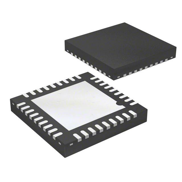


 工商网监
湘ICP备2023018690号
工商网监
湘ICP备2023018690号
