RF2163
RF21633 V,
2.5GHz Linear Power
Amplifier
3V, 2.5GHz LINEAR POWER AMPLIFIER
High Power Added Efficiency
PCS Communication Systems
Wireless LAN Systems
Commercial and Consumer Systems
Portable Battery Powered Equipment
Broadband Spread-Spectrum
Systems
NC
12
RF OUT
BIAS GND2
3
11
RF OUT
PWR SEN
4
10
RF OUT
Applications
VCC1
2
1800MHz to 2500MHz Frequency Range
2.5GHz ISM Band Applications
VCC1
RF IN
Patent Pending Power Sense
Technology
13
Bias
5
6
7
8
9
GND
19dB Small Signal Gain
14
BIAS GND 1
15
VREG2
+30dBm Saturated Output
Power
16
VREG1
Single 3.3V Power Supply
1
PWR REF
VCC
Features
GND
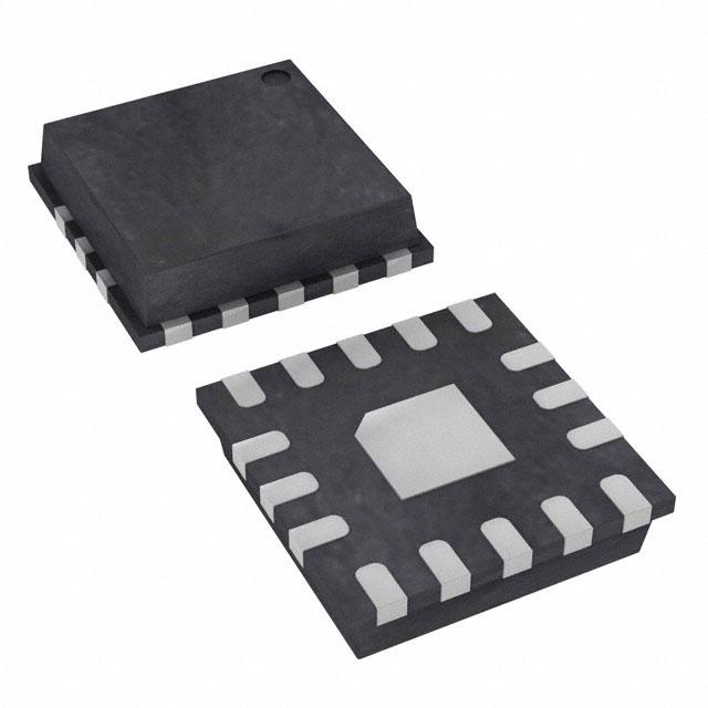
Package Style: QFN, 16-Pin, 4 x 4
Functional Block Diagram
Product Description
The RF2163 is a linear, medium power, high efficiency amplifier IC designed specifically for low voltage operation. The device is manufactured on an advanced Gallium Arsenide Heterojunction Bipolar Transistor (HBT) process, and has been
designed for use as the final RF amplifier in 2.5GHz spread-spectrum transmitters.
The device is provided in a 16-pin leadless chip carrier with a backside ground and
is self-contained with the exception of the output matching network and power supply feed line.
Ordering Information
RF2163
RF2163SR
RF2163TR7
RF2163TR13
RF2163PCK-410
GaAs HBT
GaAs MESFET
InGaP HBT
Standard 25 piece bag
Standard 100 piece reel
Standard 750 piece reel
Standard 2500 piece reel
Fully assembled evaluation board tuned for 2.4GHz to
2.5GHz and 5 loose sample pieces
Optimum Technology Matching® Applied
SiGe BiCMOS
Si BiCMOS
SiGe HBT
GaAs pHEMT
Si CMOS
Si BJT
GaN HEMT
RF MICRO DEVICES®, RFMD®, Optimum Technology Matching®, Enabling Wireless Connectivity™, PowerStar®, POLARIS™ TOTAL RADIO™ and UltimateBlue™ are trademarks of RFMD, LLC. BLUETOOTH is a trademark owned by Bluetooth SIG, Inc., U.S.A. and licensed for use by RFMD. All other trade names, trademarks and registered trademarks are the property of their respective owners. ©2006, RF Micro Devices, Inc.
DS110615
7628 Thorndike Road, Greensboro, NC 27409-9421 · For sales or technical
support, contact RFMD at (+1) 336-678-5570 or sales-support@rfmd.com.
1 of 10
�RF2163
Absolute Maximum Ratings
Parameter
Rating
Unit
Supply Voltage
-0.5 to +6.0
VDC
Power Control Voltage (VREG)
-0.5 to 3.3
V
DC Supply Current
1000
mA
Input RF Power
+15
dBm
-40 to +85
°C
-40 to +150
°C
Operating Ambient Temperature
Storage Temperature
Moisture sensitivity
JEDEC Level 3
Parameter
Min.
Specification
Typ.
Max.
Caution! ESD sensitive device.
Exceeding any one or a combination of the Absolute Maximum Rating conditions may
cause permanent damage to the device. Extended application of Absolute Maximum
Rating conditions to the device may reduce device reliability. Specified typical performance or functional operation of the device under Absolute Maximum Rating conditions is not implied.
RoHS status based on EUDirective2002/95/EC (at time of this document revision).
The information in this publication is believed to be accurate and reliable. However, no
responsibility is assumed by RF Micro Devices, Inc. ("RFMD") for its use, nor for any
infringement of patents, or other rights of third parties, resulting from its use. No
license is granted by implication or otherwise under any patent or patent rights of
RFMD. RFMD reserves the right to change component circuitry, recommended application circuitry and specifications at any time without prior notice.
Unit
Condition
T=25 °C, VCC =3.5V, VREG1 =VREG2 =2.3V,
Freq=2450MHz
Overall
Frequency Range
1800 to 2500
Maximum Saturated Output Power
+29
+30
MHz
+32
dBm
Efficiency at Max Output Power
26
%
Maximum Linear Output Power
25
dBm
Linear Efficiency
PIN =+13dBm
With 802.11 modulation (11Mbit/s) and meeting 802.11 spectral mask.
25
%
19
dB
PIN =10dBm
Reverse Isolation
30
dB
In “ON” state
30
dB
In “OFF” state
Second Harmonic
-35
dBc
Including second harmonic trap, see application circuit
Adjacent Channel Power
-35
-32
dBc
POUT =24dBm
Alternate Channel Power
-52
-50
dBc
POUT =24dBm
Isolation
TBD
dBm
In “OFF” state, PIN =TBD
Input Impedance
50
Input VSWR
2:1
Small Signal Gain
16
With external matching
With external matching
Power Down
VREG “ON”
2.3
VREG “OFF”
0
0.5
V
Voltage supplied to control input; device is
“ON”
V
Voltage supplied to control input; device is
“OFF”
Power Supply
Operating Voltage
Current Consumption
3.0 to 5.0
V
650
mA
Power Down “ON”, at max output power
350
mA
Power Down “ON”, POUT =25dBm
mA
Idle current
150
2 of 10
290
7628 Thorndike Road, Greensboro, NC 27409-9421 · For sales or technical
support, contact RFMD at (+1) 336-678-5570 or sales-support@rfmd.com.
DS110615
�RF2163
Pin
1
Function
GND
2
RF IN
Description
Interface Schematic
Ground connection. For best performance, keep traces physically short
and connect immediately to ground plane.
RF input. This input is AC coupled, so an external blocking capacitor is not
required if this pin is connected to a DC path.
VCC1
Bond Wire
Inductance
RF IN
BIAS
3
BIAS GND2
4
PWR SEN
Ground for second stage bias circuit. For best performance, keep traces
See pin 16.
physically short and connect immediately to ground plane.
The PWR SEN and PWR REF pins can be used in conjunction with an external feedback path to provide an RF power control function for the RF2163.
The power control function is based on sampling the RF drive to the final
stage of the RF2163.
RF OUT
PWR SEN
PWR REF
BIAS
5
6
7
8
PWR REF
VREG1
VREG2
BIAS GND1
9
10
GND
RF OUT
11
12
13
14
RF OUT
RF OUT
NC
VCC1
15
16
VCC1
VCC
Same as pin 4.
See pin 4.
This pin requires a regulated supply to maintain the correct bias current.
See pin 16.
Same as pin 6.
See pin 16.
Ground for first stage bias circuit. For best performance connect to ground
with a 10nH inductor.
Same as pin 1.
See pin 16.
RF output and bias for the output stage. The power supply for the output
transistor needs to be supplied to this pin. This can be done through a
quarter-wave length microstrip line that is RF grounded at the other end, or
through an RF inductor that supports the required DC currents.
RF OUT
BIAS
Same as pin 10.
See pin 10.
Same as pin 10.
See pin 10.
Not connected.
Interstage match and bias for first stage output. Connect interstage match- See pin 2.
ing capacitor to t pin with a short trace. Connect low-frequency bypass
capacitors to this pin with a long trace. See evaluation board layout for
details.
Same as pin 14.
See pin 2.
Power supply pin for the bias circuits. External low frequency bypass capacitors should be connected if no other low frequency decoupling is nearby.
VCC
VREG1
BIAS
VREG2
BIAS
GND1
Pkg
Base
DS110615
GND
Ground connection. The backside of the package should be connected to
the ground plane through a short path, i.e., vias under the device may be
required.
BIAS
GND2
See pin 1 and 2.
7628 Thorndike Road, Greensboro, NC 27409-9421 · For sales or technical
support, contact RFMD at (+1) 336-678-5570 or sales-support@rfmd.com.
3 of 10
�RF2163
Package Drawing
0.10 C B
-B-
2 PLCS
4.00
0.10 C B
3.75
2 PLCS
2.00
0.80
TYP
A
2
1.60
2 PLCS
1.50
3.75
4.00
SQ.
0.75
0.50
0.10 C A
2 PLCS
INDEX AREA
2.00
0.45
0.28
0.10 C A
2 PLCS
3.20
2 PLCS
12°
MAX
1.00
0.90
Dimensions in mm.
Shaded pin is lead 1.
4 of 10
0.05
0.00
0.10 M C A B
C
0.05
0.75
0.65
7628 Thorndike Road, Greensboro, NC 27409-9421 · For sales or technical
support, contact RFMD at (+1) 336-678-5570 or sales-support@rfmd.com.
DS110615
�RF2163
Application Schematic
2400MHz to 2483MHz
VCC
10 uF
Part is Backside Grounded.
1000 pF
1000 pF
1000 pF
1
6.2 pF
16
15
14
13
15 nH
10 pF
1.5 pF
RF IN
2
12
3.0 pF
10 pF
1.5 nH
3
11
Bias
4
5
6
RF OUT
TL1
3.0 pF
TL2
1.5 pF
10
7
8
9
390 :
VREG1 = 2.4 V
VREG2 = 2.4 V
VCC = 3.5 V
1000 pF
10 nH
390 :
1000 pF
1000 pF
Transmission
Line Length
1000 pF
PWR SEN
1000 pF
10 uF
TL1
TL2
25 mil
175 mil
10 uF
WL)L
PWR REF
VREG1
DS110615
VREG2
7628 Thorndike Road, Greensboro, NC 27409-9421 · For sales or technical
(+1) 336-678-5570
336-678-5570 or sales-support@rfmd.com.
sales-support@rfmd.com
support, contact RFMD at (+1)
5 of 10
�RF2163
Evaluation Board Schematic
2400MHz to 2483MHz
VCC
10 uF
Part is Backside Grounded.
1000 pF
1000 pF
1000 pF
1
6.2 pF
16
15
14
13
15 nH
10 pF
1.5 pF
RF IN
2
12
3.0 pF
10 pF
1.5 nH
3
11
Bias
4
5
6
RF OUT
TL1
3.0 pF
TL2
1.5 pF
10
7
8
9
390 :
VREG1 = 2.4 V
VREG2 = 2.4 V
VCC = 3.5 V
1000 pF
10 nH
390 :
1000 pF
1000 pF
Transmission
Line Length
1000 pF
PWR SEN
1000 pF
10 uF
TL1
TL2
25 mil
175 mil
10 uF
WL)L
PWR REF
VREG1
6 of 10
VREG2
7628 Thorndike Road, Greensboro, NC 27409-9421 · For sales or technical
support, contact RFMD at (+1) 336-678-5570 or sales-support@rfmd.com.
(+1) 336-678-5570
sales-support@rfmd.com
DS110615
�RF2163
Evaluation Board Layout
Board Size 2.0” x 2.0”
Board Thickness 0.028”, Board Material FR-4
DS110615
7628 Thorndike Road, Greensboro, NC 27409-9421 · For sales or technical
support, contact RFMD at (+1) 336-678-5570 or sales-support@rfmd.com.
7 of 10
�RF2163
Theory of Operation and Application Information
The RF2163 is a two-stage device with a nominal gain of 19dB in the 2.4GHz to 2.5GHz ISM band. The RF2163 is designed
primarily for IEEE802.11B WiFi applications where the available supply voltage and current are not limited. It will meet
802.11B spectral mask requirements at an output power of +24dBm. It is especially appropriate for WiFi access points and
other base-station type equipment.
The RF2163 requires only a single positive supply of 3.3V nominal (or greater) to operate to full specifications. Power control is
provided through two bias control input pins (VREG1 and VREG2), but in most applications these are tied together and used as a
single control input.
There is some external matching on the input and output of the part, thus allowing the part to be used in other applications
outside the 2.4GHz to 2.5GHz ISM band (such as MMDS). Both the input and the output of the device need a series DC-blocking capacitor. In some cases, a capacitor used as a matching component can also serve as the blocking cap. The circuit used
on the evaluation board is optimized for 3.5V nominal applications.
For best results, the PA circuit layout from the evaluation board should be copied as closely as possible, particularly the ground
layout and ground vias. Other configurations may also work, but the design process is much easier and quicker if the layout is
copied from the RF2163 evaluation board. Gerber files of our designs can be provided upon request.
The RF2163 is not a difficult part to implement, but care in circuit layout and component selection is always advisable when
designing circuits to operate at 2.5GHz. The most critical passive components in the circuit are the input, interstage and output matching components (C1, C5, C6, C7, and C11). In these cases, high-Q capacitors suitable for RF applications are used
on our evaluation board (a BOM is available on request). High-Q parts are not required in every design, but it is very strongly
recommended that the original design be implemented with the same or similar parts used on our evaluation board. Then, less
costly components can be substituted in their place, making it easy to test the impact of cheaper components on performance.
General RFMD experience has indicated that the slightly higher cost of better quality passive components is more than offset
by the significant improvements in production yields in large-volume manufacturing.
The interstage matching capacitor, C11, along with the combined inductance of the internal bond wire, the short length of circuit board trace, and the parasitic inductance of this capacitor, tunes the peak of the small-signal gain response. The trace
length between C11 and pins 14 and 15 should be kept as short as possible.
In practice, VCC1, VCC, and the supply for the output stage bias will be tied to this supply line. This can be accomplished using a
suitably-long transmission line which is RF shorted on the other end. Ideally the length of this line will be a quarter wavelength,
but it only needs to be long enough so that the effects of other supply bypass capacitors on the interstage match are minimized. If board space is a concern, this isolation can also be accomplished with an RF choke inductor or ferrite bead. Additionally, a higher-value capacitor than shown on the application schematic can be used if bypass capacitors must be closer. A
Smith Chart can be used to provide initial guidance for value selection and parts placement. Be aware of the self-resonant frequency (SRF) of higher-valued capacitors. The SRF must be above the frequency of operation.
The output matching caps are C5, C6, and C7. These are tuned along with the 50 transmission line segments TL1 and TL2,
as shown on the evaluation board schematic. These segments should be duplicated as closely as possible. Due to variations in
FR-4 characteristics and PCB manufacturer process variations, some benefit will be obtained from small adjustments to these
transmission line lengths when the evaluation board layout is duplicated on another design. Prior to full rate manufacturing,
the board layout of early prototypes should include some additional exposed ground areas around C5, C6, and C7 to optimize
this part of the circuit. In order to reduce component count, the output can also be tuned with a single capacitor. A Smith Chart
can help determine the desired value and transmission line length, which can be similarly adjusted on the board prior to production. This will result in a slightly lower-bandwidth and more sensitive match, but in most applications the bandwidth is still
sufficient.
8 of 10
7628 Thorndike Road, Greensboro, NC 27409-9421 · For sales or technical
support, contact RFMD at (+1) 336-678-5570 or sales-support@rfmd.com.
DS110615
�RF2163
Power sensing is implemented with the PWR SEN and PWR REF lines. The outputs of these pins are transistor collectors and
need to be pulled up to the supply through a resistor. PWR REF provides an output current proportional to the output stage bias
current, and PWR SEN provides an output current proportional to the total (RF and bias) current of the output stage. The pulllup resistors convert these currents to voltages, and the voltage difference between these two pins is proportional to the RF
current. See the graph, “VREF -VSENSE versus POUT”, for the response of this signal. This difference signal can be fed to a power
control circuit elsewhere in the end product, or it can be processed at the PA with additional circuitry and used to adjust the
VREG voltage(s) to implement automatic level control. Contact RFMD Sales or Applications Engineering for additional data and
guidance in using this feature.
The RF2163 has primarily been characterized with a voltage on VREG1 and VREG2 of 2.4VDC. However, the RF2163 will operate
from a wide range of control voltages. If you prefer to use a control voltage that is significantly different than 2.4VDC, contact
RFMD Sales or Applications Engineering for additional data and guidance.
DS110615
7628 Thorndike Road, Greensboro, NC 27409-9421 · For sales or technical
support, contact RFMD at (+1) 336-678-5570 or sales-support@rfmd.com.
9 of 10
�RF2163
ICC versus POUT
VREF - VSENSE versus POUT
1200.0
0.5
1000.0
800.0
-0.5
ICC (mA)
Log10 (V REF-VSENSE )
0.0
600.0
-1.0
400.0
-1.5
200.0
0.0
-2.0
-5.0
0.0
5.0
10.0
15.0
20.0
25.0
30.0
35.0
-5.0
0.0
5.0
10.0
15.0
20.0
25.0
30.0
35.0
POUT (dBm)
POUT (dBm)
Gain and Efficiency versus POUT with 802.11 Modulation
45.0
40.0
Gain, Efficiency (dB, %)
35.0
30.0
25.0
20.0
15.0
10.0
Gain (dB)
5.0
Eff
0.0
-5.0
0.0
5.0
10.0
15.0
20.0
25.0
30.0
35.0
POUT (dBm)
10 of 10
7628 Thorndike Road, Greensboro, NC 27409-9421 · For sales or technical
support, contact RFMD at (+1) 336-678-5570 or sales-support@rfmd.com.
DS110615
�