TGA4531
K-Band High Linearity Power Amplifier
Key Features
•
•
•
•
•
•
•
•
•
Measured Performance
Frequency Range: 17 - 24 GHz
Power: 32 dBm Psat, 31 dBm P1dB
Gain: 23 dB
TOI: 40 dBm
NF: 6 dB
Return Loss: -15 dB
Bias: Vd = 7 V, Id = 720 mA, Vg = -0.65 V Typical
Technology: 3MI 0.25 um mmw Power pHEMT
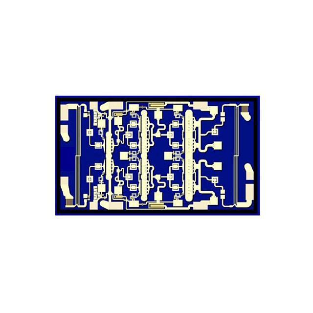
Chip Dimensions: 2.51 x 1.45 x 0.1 mm
Primary Applications
Bias conditions: Vd = 7 V, Id = 720 mA, Vg = -0.65 V Typical
•
•
Point-to-Point Radio
K-Band Sat-Com
Product Description
The TriQuint TGA4531 is High Linearity Power
Amplifier for K-band applications. The part is
designed using TriQuint’s proven standard 0.25 um
gate Power pHEMT production process.
The TGA4531 provides a nominal 32 dBm of
output power at an input power level of 15 dBm
with a small signal gain of 23 dB. Nominal TOI is
40 dBm and noise figure is 6 dB.
The part is ideally suited for low cost emerging
markets such as Point-to-Point Radio, and K-band
Satellite Communications.
1
TriQuint Semiconductor: www. triquint.com (972)994-8465 Fax (972)994-8504 Info-mmw@tqs.com
Aug 2010 © Rev A
�TGA4531
Table I
Absolute Maximum Ratings 1/
Symbol
Parameter
Vd-Vg
Value
Drain to Gate Voltage
Vd
Drain Voltage
Vg
Gate Voltage Range
Id
Drain Current
Ig
Gate Current Range
Pin
Tchannel
Notes
10.5 V
8V
2/
-2.5 to 0 V
1.25 A
2/
-7 to 32 mA
Input Continuous Wave Power
26 dBm
Channel Temperature
200 °C
2/
1/
These ratings represent the maximum operable values for this device. Stresses beyond those listed
under “Absolute Maximum Ratings” may cause permanent damage to the device and / or affect
device lifetime. These are stress ratings only, and functional operation of the device at these
conditions is not implied.
2/
Combinations of supply voltage, supply current, input power, and output power shall not exceed the
maximum power dissipation listed in Table IV.
Table II
Recommended Operating Conditions
Symbol
Value
Vd
Drain Voltage
7V
Id
Drain Current
720 mA
Drain Current under RF Drive
1.12 A
Gate Voltage
-0.65 V
Id_Drive
Vg
1/
Parameter 1/
See assembly diagram for bias instructions.
2
TriQuint Semiconductor: www. triquint.com (972)994-8465 Fax (972)994-8504 Info-mmw@tqs.com
Aug 2010 © Rev A
�TGA4531
Table III
RF Characterization Table
Bias: Vd = 7 V, Id = 720 mA, Vg = -0.65 V Typical
SYMBOL
PARAMETER
TEST
CONDITIONS
MIN
NOMINAL
21
23
MAX
UNITS
Gain
Small Signal Gain
F = 17.7 – 23.6 GHz
IRL
Input Return Loss
F = 17.7 – 23.6 GHz
-15
-10
dB
ORL
Output Return Loss
F = 17.7 – 23.6 GHz
-15
-10
dB
Psat
Saturated Output
Power
F = 17.7 – 23.6 GHz
P1dB
Output Power @ 1dB
Compression
F = 17.7 – 23.6 GHz
TOI
Output TOI
F = 17.7 – 23.6 GHz
NF
Noise Figure
Gain Temperature
Coefficient
31
dB
32
dBm
31
dBm
40
dBm
F = 17.7 – 23.6 GHz
6
dB
F = 17.7 – 23.6 GHz
-0.04
dB/°C
37
3
TriQuint Semiconductor: www. triquint.com (972)994-8465 Fax (972)994-8504 Info-mmw@tqs.com
Aug 2010 © Rev A
�TGA4531
Table IV
Power Dissipation and Thermal Properties
Parameter
Test Conditions
Value
Maximum Power Dissipation
Tbaseplate = 70 °C
Pd = 10 W
Tchannel = 199 °C
Thermal Resistance, θjc
Vd = 7 V
Id = 720 mA
Pd = 5.04 W
Tbaseplate = 70 ºC
θjc = 12.9 °C/W
Tchannel = 135 °C
Tm = 3.8E+6 Hrs
Thermal Resistance, θjc
Under RF Drive
Vd = 7 V
Id = 1.12 A
Pout = 32 dBm
Pd = 6.25 W
Tbaseplate = 70 ºC
θjc = 12.9 °C/W
Tchannel = 150 °C
Tm = 1.0E+6 Hrs
Mounting Temperature
30 Seconds
Storage Temperature
320 °C
-65 to 150 °C
Median Lifetime (Tm) vs. Channel Temperature
4
TriQuint Semiconductor: www. triquint.com (972)994-8465 Fax (972)994-8504 Info-mmw@tqs.com
Aug 2010 © Rev A
�TGA4531
Measured Data
Bias conditions: Vd = 7 V, Id = 720 mA, Vg = -0.65 V Typical
5
TriQuint Semiconductor: www. triquint.com (972)994-8465 Fax (972)994-8504 Info-mmw@tqs.com
Aug 2010 © Rev A
�TGA4531
Measured Data
Bias conditions: Vd = 7 V, Id = 720 mA, Vg = -0.65 V Typical
6
TriQuint Semiconductor: www. triquint.com (972)994-8465 Fax (972)994-8504 Info-mmw@tqs.com
Aug 2010 © Rev A
�TGA4531
Measured Data
Bias conditions: Vd = 7 V, Id = 720 mA, Vg = -0.65 V Typical
7
TriQuint Semiconductor: www. triquint.com (972)994-8465 Fax (972)994-8504 Info-mmw@tqs.com
Aug 2010 © Rev A
�Measured Data
TGA4531
Bias conditions: Vd = 7 V, Id = 720 mA, Vg = -0.65 V Typical
8
TriQuint Semiconductor: www. triquint.com (972)994-8465 Fax (972)994-8504 Info-mmw@tqs.com
Aug 2010 © Rev A
�TGA4531
Measured Data
Bias conditions: Vd = 7 V, Id = 720 mA, Vg = -0.65 V Typical
9
TriQuint Semiconductor: www. triquint.com (972)994-8465 Fax (972)994-8504 Info-mmw@tqs.com
Aug 2010 © Rev A
�TGA4531
Measured Data
Bias conditions: Varies
10
TriQuint Semiconductor: www. triquint.com (972)994-8465 Fax (972)994-8504 Info-mmw@tqs.com
Aug 2010 © Rev A
�Measured Data
TGA4531
Bias conditions: Varies
11
TriQuint Semiconductor: www. triquint.com (972)994-8465 Fax (972)994-8504 Info-mmw@tqs.com
Aug 2010 © Rev A
�TGA4531
Electrical Schematic
Vd_Top
Vd_Bottom
3
5
TGA4531
RF Input
1
4
2
RF Output
6
Vg_Top
Vg_Bottom
Bias Procedures
Bias-up Procedure
Bias-down Procedure
Vg set to -1.5 V
Turn off RF supply
Vd_set to +7 V
Reduce Vg to -1.5V. Ensure Id ~ 0 mA
Adjust Vg more positive until quiescent Id is 720 mA.
This will be ~ Vg = -0.65 V
Turn Vd to 0 V
Apply RF signal to input
Turn Vg to 0 V
12
TriQuint Semiconductor: www. triquint.com (972)994-8465 Fax (972)994-8504 Info-mmw@tqs.com
Aug 2010 © Rev A
�TGA4531
Mechanical Drawing
Units: millimeters
Thickness: 0.10
Die x,y size tolerance: +/- 0.050
Chip edge to bond pad dimensions are shown to center of pad
Ground is backside of die
Bond Pad #1
RF In
0.100 x 0.200
Bond Pad #4
RF Out
0.100 x 0.200
Bond Pad #2
Vg_Top
0.100 x 0.100
Bond Pad #5
Vd_Bottom
0.180 x 0.100
Bond Pad #3
Vd_Top
0.180 x 0.100
Bond Pad #6
Vg_Bottom
0.100 x 0.100
GaAs MMIC devices are susceptible to damage from Electrostatic Discharge. Proper precautions should
be observed during handling, assembly and test.
13
TriQuint Semiconductor: www. triquint.com (972)994-8465 Fax (972)994-8504 Info-mmw@tqs.com
Aug 2010 © Rev A
�TGA4531
Recommended Assembly Diagram
-0.65V Typical
7V, 720mA
Vg
Vd
15Ω
15Ω
1 μF
1 μF
0.01 uF
RF IN
100 pF
0.01 uF
100 pF
RF OUT
100 pF
0.01 uF
Vd
1 μF
Vg can be biased from either side. Vd must be biased from both sides.
GaAs MMIC devices are susceptible to damage from Electrostatic Discharge. Proper precautions should
be observed during handling, assembly and test.
TriQuint Semiconductor: www. triquint.com (972)994-8465 Fax (972)994-8504 Info-mmw@tqs.com
Aug 2010 © Rev A
14
�TGA4531
Assembly Notes
Component placement and adhesive attachment assembly notes:
• Vacuum pencils and/or vacuum collets are the preferred method of pick up.
• Air bridges must be avoided during placement.
• The force impact is critical during auto placement.
• Organic attachment (i.e. epoxy) can be used in low-power applications.
• Curing should be done in a convection oven; proper exhaust is a safety concern.
Reflow process assembly notes:
• Use AuSn (80/20) solder and limit exposure to temperatures above 300°C to 3-4 minutes, maximum.
• An alloy station or conveyor furnace with reducing atmosphere should be used.
• Do not use any kind of flux.
• Coefficient of thermal expansion matching is critical for long-term reliability.
• Devices must be stored in a dry nitrogen atmosphere.
Interconnect process assembly notes:
• Thermosonic ball bonding is the preferred interconnect technique.
• Force, time, and ultrasonics are critical parameters.
• Aluminum wire should not be used.
• Devices with small pad sizes should be bonded with 0.0007-inch wire.
Ordering Information
Part
Package Style
TGA4531
GaAs MMIC Die
GaAs MMIC devices are susceptible to damage from Electrostatic Discharge. Proper precautions should
be observed during handling, assembly and test.
15
TriQuint Semiconductor: www. triquint.com (972)994-8465 Fax (972)994-8504 Info-mmw@tqs.com
Aug 2010 © Rev A
�
很抱歉,暂时无法提供与“TGA4531”相匹配的价格&库存,您可以联系我们找货
免费人工找货