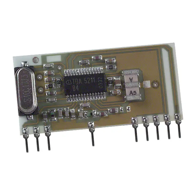
FM TRANSMITTER & RECEIVER
HYBRID MODULES.
•
•
•
•
•
•
•
•
FM-RTFQ SERIES
FM-RRFQ SERIES
FM Radio Transmitter & Receivers
Available As 315 or 433 or 868MHz
Transmit Range Up To 250m
Miniature Packages
Data Rate upto 9.6Kbps
RTFQ1
No Adjustable Components
Very Stable Operating Frequency
Operates from –20 to +850C
Transmitter
•
•
3-12 Supply Voltage
SIL or DIL Package
RRFQ1
Receiver
•
•
•
•
•
PLL XTAL Design
CMOS/TTL Output
RSSI Output
Standby Mode (max 100nA)
5V Supply Voltage
RTFQ2
Applications
•
•
•
•
•
•
Wireless Security Systems
Car Alarms
Remote Gate Controls
Remote Sensing
RRFQ2
Data Capture
Sensor Reporting
Description
These miniature RF modules provide a cost effective high performance FM Radio data link, at either 315,
433.92 or 868MHz. Manufactured using laser trimmed Thick Film ceramic Hybrid the modules exhibits
extremely stable electronic characteristics over an Industrial Temperature range. The hybrid technology uses
no adjustable components and ensures very reliable operation.
This transmitter and receiver pair enables the simple implementation of a data link at distances upto 75 metres
in-building and 250 metres open ground.
These modules will suit one-to-one and multi-node wireless links in applications including car and building
security, EPOS and inventory tracking, remote industrial process monitoring and computer networking.
Because of their small size and low power requirements, both modules are ideal for use in portable, batterypowered applications such as hand-held terminals.
DS069-8 May 04
©2004 Reg. No. 227 4001, England
Page 1
�FM TRANSMITTER & RECEIVER
HYBRID MODULES.
FM-RTFQ SERIES
FM-RRFQ SERIES
Transmitters
There are two versions of transmitter:
RTFQ1;
A Dual in Line Package operating at 3.3V. This provides the most rugged mechanical fixing to
the host PCB. Power Down mode is also available.
RTFQ2;
A Single in Line Package incorporating a voltage regulator for 3-12V operation. (Compatible
with many other RF transmitter modules available)
Transmitter Block Diagram
In
XTAL
Oscillator
XTAL
PLL
Synthesizer
Power Amp
Out
En
Part Numbering
Part Number
FM-RTFQ1-315
FM-RTFQ1-433
Description
DIL FM Transmitter Module 315 MHz
DIL FM Transmitter Module 433.92 MHz
FM-RTFQ1-868
DIL FM Transmitter Module 868.35 MHz
FM-RTFQ2-433R
SIL FM Transmitter Module 433.92 MHz 3-12V I/P
FM-RTFQ2-868R
SIL FM Transmitter Module 868.35 MHz 3-12V I/P
Receivers
There are two versions of receiver:
RRFQ1:
A Single in Line Package with sleep / Power down mode.
RRFQ2:
A Single in Line Package, pin compatible with many other receivers
Receiver Block Diagram
Vcc
Vcc
In
Pre Amp
Filter
Mixer
10.7MHz
IF Filter
FM
Demodulator
Comparator
Out
GND
PLL
Synthesizer
GND
GND
Part Numbering
DS069-8 May 04
Part Number
FM-RRFQ1-315
FM-RRFQ1-433
Description
SIL FM Receiver Module 315 MHz
SIL FM Receiver Module 433.92 MHz
FM-RRFQ1-868
SIL FM Receiver Module 868.35 MHz
FM-RRFQ2-433
SIL FM Receiver Module 433.92 MHz
FM-RRFQ2-868
SIL FM Receiver Module 868.35 MHz
©2004 Reg. No. 227 4001, England
Page 2
�FM TRANSMITTER & RECEIVER
HYBRID MODULES.
FM-RTFQ SERIES
FM-RRFQ SERIES
RTFQ1 Mechanical Dimensions
20.32mm
PCB Layout Requirements
1
Top View
(Components
Underneath)
5.08mm
2
3
2.54mm
Module Thickness 2mm
6
11.43mm
5
4
Pins on "0.1 pitch
Pin Dimensions :
0.25mm x 0.50mm
20mm
RTFQ2 Mechanical Dimensions
PCB Layout Requirements
30.48mm
10.67mm
2.54
1mm
20.32mm
2.54 spacing
Module Thickness 2mm
Pins on "0.1 pitch
RTFQ2
1 2
Pin Dimensions :
0.25mm x 0.50mm
3 4 5
Pin Description
RTFQ1
1
2
3
4
5
6
RTFQ2
N/A
5
1
3
4
2
Name
En
IN
GND
Vcc
GND
EA
Description
Enable (active high)
Data input
Ground, Connect to RF earth return path
Supply Voltage
Ground, Connect to RF earth return path
External Antenna
Technical Specifications
Electrical Characteristics
Supply Voltage RTFQ1
Supply Voltage RTFQ2
Supply Current
Standby Current (IN = EN = Low)
MIN
2.1
2.5
7
Frequency
RF Output into 50Ω (Vcc=3.3V)
Initial Frequency Accuracy
FM Deviation
Harmonic Spurious Emissions
Input High Voltage RTFQ1
Input High Voltage RTFQ2
Power up Time (En to full RF)
Power up Time (Power on to full RF)
Max Data Rate
Operating Temperature
DS069-8 May 04
TYPICAL
3.3
-35
25
315.0
433.92
868.35
+5 / +5 / +1
0
30
-50
1.5
1.5
-25
©2004 Reg. No. 227 4001, England
MAX
4.00
12.00
8
100
DIMENSION
V
V
mA
nA
MHz
+35
35
Vcc
5.5
1
5
9.6
+80
Page 3
dBm
KHz
KHz
dBc
V
V
mS
mS
KHz
°C
�FM TRANSMITTER & RECEIVER
HYBRID MODULES.
FM-RTFQ SERIES
FM-RRFQ SERIES
RRFQ1 Mechanical Details
38.1mm
4mm
Component Side
1
3
7
18.3mm
11
15
Pin Dimensions :
0.25mm x 0.50mm
2.54mm
RRFQ2 Mechanical Details
45.72mm
3mm
Component Side
1 2
16.5mm
14
18
1mm
Pin Dimensions :
0.25mm x 0.50mm
2.54mm
Pin Description
RRFQ1
1
2, 7,11
3
12
13
N/A
14
15
RRFQ2
16
2,15
1
14
17
18
N/A
RSSI Output
Pin Description
+Vcc
GND
Data In (Antenna)
NC
Received Signal Strength Output
AF Output
Data Out
Power Down
0V = Standby
5V = Operating
RF In (dBm)
-120
-110
-100
-90
-80
-70
-60
-50
-40
RSSI (V)
1.20
1.32
1.50
1.78
2.06
2.35
2.62
2.72
2.75
Technical Specifications
Electrical Characteristics
Supply Voltage (Vcc)
Supply Current (Operating)
Supply Current (Standby)
Min
4.5
Max
5.5
6.8
100
315.00
433.92
868.35
Receiver Frequency
R.F Sensitivity (100% AM)
315 ,433MHZ versions
868MHz versions
3dB Bandwidth
Data Rate
Turn on Time
Turn on Time
Level of Emitted Spectrum
Low Level Output Voltage
High Level Output Voltage
Operating Temperature Range
Typical
5
5.7
dBm
9,600
5
8
-70
0.8
Vcc-1
-25
+80
KHz
Hz
mSecs
mSecs
dBm
V
V
o
C
Notes
1. Time from PD pin going high to stable data. (RRFQ1 only)
2. Time from Poer ON to stable data.
DS069-8 May 04
©2004 Reg. No. 227 4001, England
Notes
MHz
-103
-100
+/-150
300
Dimension
V
mA
nA
Page 4
1
2
I = 200uA
I = 200uA
�FM TRANSMITTER & RECEIVER
HYBRID MODULES.
FM-RTFQ SERIES
FM-RRFQ SERIES
Typical Application
The following circuits show a remote control system with ‘self learning feature’ for more information
please see Datasheet DS600
Transmitter Circuit
3.3V
Antenna
3.3V
SW1-4
1
2
3
4
A0
Vcc
A1
LED
A2
DATA
A3
GND
2K2
8
1
7
6
5
BC848
10K
EN
ANT
2
IN
3
GND
6
5
GND
4
Vcc
RTFQ1-XXX
RF600E
Receiver Circuit
Vcc
15KΩ
1KΩ
13
L
Status
LED
FM -RRFQ1
12 3
7
11
Option
Link
15
12
14
4
17
Sleep Vcc Vcc OP1
O/P 1
18
LKIN
O/P 2
OP2
M
1
O/P 3
OP3
OP4
10
LRN
RF600D
LB
1KΩ
SD1
Learn
Switch
2
O/P 4
3
Transmitter
Low Battery
Serial Data
Output
11
Vcc
9
ECLK
IN
GND
7
22KΩ
5
Prototyping Hints:
It is essential when building any Low Power Radio System that you have a ‘clean’ DC power source. Typically
the ripple voltage should be less than 10mV Peak to Peak. Normally a 470uF decoupling capacitor is sufficient
de-coupling for an AC derived DC power source.
Never place a Transmitter or Receiver directly into Vero-Board or any similar prototyping board. This will
severely restrict the range. Rather, use small lengths of wire from the prototyping board to the pins of the
Transmitter or Receiver.
A useful antenna, for testing purposes, for both the Transmitter and Receiver on 433MHz is to use a piece of
wire 17.3cm long (23.8cm at 315MHz) soldered directly to the antenna pin.
For more information or general enquiries, please contact;
RF Solutions Ltd.,
Unit 21, Cliffe Industrial Estate,
South Street, Lewes, E Sussex, BN8 6JL. England
Tel +44 (0)1273 898 000
Fax +44 (0)1273 480 661
Email sales@rfsolutions.co.uk
http://www.rfsolutions.co.uk
RF Solutions is a member of the Low Power Radio Association
All Trademarks acknowledged and remain the property of the respected owners
Information contained in this document is believed to be accurate, however no representation or warranty is given and R.F. Solutions Ltd. assumes no liability with respect to the accuracy of such
information. Use of R.F.Solutions as critical components in life support systems is not authorised except with express written approval from R.F.Solutions Ltd.
DS069-8 May 04
©2004 Reg. No. 227 4001, England
Page 5
�
很抱歉,暂时无法提供与“FM-RRFQ1-315P”相匹配的价格&库存,您可以联系我们找货
免费人工找货