®
RT2528
120mΩ
Ω, 2.5A Power Switch with Adjustable Current Limit
General Description
Features
The RT2528 is a cost effective, low voltage, P-MOSFET
power switch IC with an adjustable current limit feature.
Low on-resistance (74mΩ typ.) and low supply current
(120μA typ.) are designed in this IC.
The RT2528 can offer an adjustable current limit threshold
between 0.5A and 2.5A (typ.) via an external resistor. The
±10% current limit accuracy can be realized for all current
limit settings.
The RT2528 is an ideal solution for power supply
applications since it is functional for various current limit
requirements. The RT2528 is available in the thermal
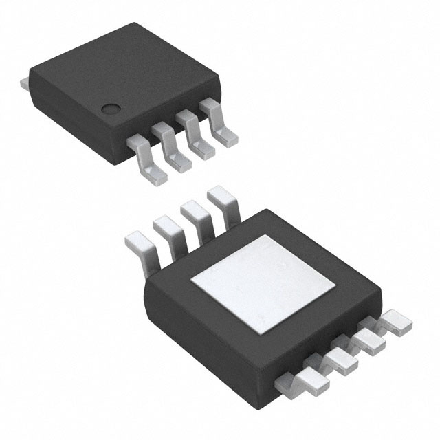
enhanced SOP-8 (Exposed Pad) package.
Adjustable Current Limit : 0.5A to 2.5A (typ.)
±10% Current Limit Accuracy @ 2A Over
Temperature
120mΩ
Ω P-MOSFET
Low Supply Current : 120μ
μA
Input Operating Voltage Range : 2.5V to 5.5V
Reverse Input-Output Voltage Protection
Built-in Soft-Start
AEC-Q100 Grade 3 Certification
RoHS Compliant and Halogen Free
Applications
Ordering Information
RT2528
Package Type
SP : SOP-8 (Exposed Pad-option 2)
Lead Plating System
G : Green (Halogen Free and Pb Free)
Automotive Audio, Navigation & Info Systems
Industrial Grade General Purpose Point of Load
Digital Set Top Boxes
Vehicle Electronics
Pin Configurations
(TOP VIEW)
Note :
Richtek products are :
VOUT
RoHS compliant and compatible with the current requirements of IPC/JEDEC J-STD-020.
Suitable for use in SnPb or Pb-free soldering processes.
8
VOUT
2
ILIM
3
FAULT
4
GND
9
VIN
7
VIN
6
GND
5
EN
SOP-8 (Exposed Pad)
Marking Information
RT2528GSP : Product Number
RT2528
GSPYMDNN
YMDNN : Date Code
Simplified Application Circuit
VIN
VIN
CIN
VOUT
COUT
RT2528
VOUT
RILIM
ILIM
Enable
EN
Copyright © 2013 Richtek Technology Corporation. All rights reserved.
DS2528-03
November 2013
GND
is a registered trademark of Richtek Technology Corporation.
www.richtek.com
1
�RT2528
Functional Pin Description
Pin No.
1, 2
Pin Name
VOUT
3
ILIM
4
FAULT
5
EN
6,
GND
9 (Exposed Pad)
7, 8
VIN
Pin Function
Output.
Current Limit Setting. Connect an external resistor to set current limit threshold.
The recommended resistance range is 10k RILIM 49.9k.
Active-Low Open-Drain Output. Asserted during over-current, over-temperature, or
reverse-voltage conditions.
Enable Control Input. Logic high turns on the power switch.
Ground. The exposed pad must be soldered to a large PCB and connected to GND
for maximum power dissipation.
Power Input. Connect a 10F or greater ceramic capacitor from the VIN to GND as
close to the IC as possible.
Function Block Diagram
Reverse Voltage
Comparator
+
Switch
well
-
Current
Sense
VIN
VOUT
4ms
Deglitch
EN
Drive
Current
Limit
FAULT
UVLO
Thermal
Sense
7.5ms
Deglitch
GND
ILIM
Operation
The RT2528 is a current-limited power switch using
P-MOSFETs for applications where short-circuit or heavy
capacitive loads will be encountered. These devices allow
users to adjust the current limit threshold between 500mA
and 2.5A (typ.) via an external resistor. Additional device
shutdown features include over-temperature protection and
reverse-voltage protection.
Copyright © 2013 Richtek Technology Corporation. All rights reserved.
www.richtek.com
2
The RT2528 provides built-in soft-start function. The driver
controls the gate voltage of the power switch. The driver
incorporates circuitry that controls the rising time and
falling time of the output voltage to limit large inrush current
and voltage surges. The RT2528 enters constant-current
mode when the load exceeds the current limit threshold.
is a registered trademark of Richtek Technology Corporation.
DS2528-03
November 2013
�RT2528
Absolute Maximum Ratings
(Note 1)
Supply Input Voltage, VIN ----------------------------------------------------------------------------------------------Other Pins ------------------------------------------------------------------------------------------------------------------Power Dissipation, PD @ TA = 25°C
SOP-8 (Exposed Pad) --------------------------------------------------------------------------------------------------Package Thermal Resistance (Note 2)
SOP-8 (Exposed Pad), θJA ---------------------------------------------------------------------------------------------SOP-8 (Exposed Pad), θJC --------------------------------------------------------------------------------------------Lead Temperature (Soldering, 10 sec.) ------------------------------------------------------------------------------Junction Temperature ----------------------------------------------------------------------------------------------------Storage Temperature Range -------------------------------------------------------------------------------------------ESD Susceptibility (Note 3)
HBM (Human Body Model) ----------------------------------------------------------------------------------------------
Recommended Operating Conditions
−0.3V to 6V
−0.3V to 6V
2.041W
49°C/W
8°C/W
260°C
150°C
−65°C to 150°C
2kV
(Note 4)
Supply Input Voltage, VIN ----------------------------------------------------------------------------------------------- 2.5V to 5.5V
Temperature Range Junction -------------------------------------------------------------------------------------------- −40°C to 125°C
Ambient Temperature Range -------------------------------------------------------------------------------------------- −40°C to 85°C
Electrical Characteristics
(VIN = 5V, TA = −40°C to 85°C, unless otherwise specified)
Parameter
Symbol
Test Conditions
Min
Typ
Max
Unit
Shutdown Current
ISHDN
VEN = 0V, IOUT = 0A
--
1
5
A
Quiescent Current
IQ
IOUT = 0A
--
120
300
A
EN Input
Voltage
Logic-High
VIH
1.2
--
--
Logic-Low
VIL
--
--
0.4
--
0.02
0.5
A
10
--
65
k
--
1
10
A
--
160
--
°C
EN Input Current
IEN
Current Limit Setting
Resistor Range
RILIM
Reverse Leakage Current
IREV
Thermal Shutdown
Threshold
TSD
Static Drain-Source
On-State Resistance
RDS(ON)
IOUT = 0.2A
--
74
120
m
Reverse Voltage
Comparator Trip Point
IREV_HYS
VOUT VIN
100
135
300
mV
RILIM = 13k
1800
2000
2200
RILIM = 13k, TA = 25°C
1840
2000
2160
RILIM = 49.9k
468
520
572
2
7.5
14
Current Limit
FAULT Deglitch
ILIM
VIN = 5.5V VEN = 0V or 5.5V
V
VOUT = 5V, VIN = 0V
FAULT assertion or de-assertion due to
over-current condition
Copyright © 2013 Richtek Technology Corporation. All rights reserved.
DS2528-03
November 2013
mA
ms
is a registered trademark of Richtek Technology Corporation.
www.richtek.com
3
�RT2528
Note 1. Stresses beyond those listed “Absolute Maximum Ratings” may cause permanent damage to the device. These are
stress ratings only, and functional operation of the device at these or any other conditions beyond those indicated in
the operational sections of the specifications is not implied. Exposure to absolute maximum rating conditions may
affect device reliability.
Note 2. θJA is measured at TA = 25°C on a high effective thermal conductivity four-layer test board per JEDEC 51-7. θJC is
measured at the exposed pad of the package. The PCB copper area with exposed pad is 70mm2.
Note 3. Devices are ESD sensitive. Handling precaution is recommended.
Note 4. The device is not guaranteed to function outside its operating conditions.
Copyright © 2013 Richtek Technology Corporation. All rights reserved.
www.richtek.com
4
is a registered trademark of Richtek Technology Corporation.
DS2528-03
November 2013
�RT2528
Typical Application Circuit
VIN
RFAULT
100k
FAULT Signal
Enable
1, 2
7, 8
VOUT
VIN
CIN
COUT
10µF
22µF
RT2528
RILIM
13k
3
ILIM
4 FAULT
5
6, 9 (Exposed Pad)
EN
GND
VOUT
Note : RILIM = 13kΩ for 2A Power Switch Operation
Copyright © 2013 Richtek Technology Corporation. All rights reserved.
DS2528-03
November 2013
is a registered trademark of Richtek Technology Corporation.
www.richtek.com
5
�RT2528
Typical Operating Characteristics
Quiescent Current vs. Input Voltage
190
140
170
Quiescent Current (µA) 1
Quiescent Current (µA) 1
Quiescent Current vs. Temperature
150
130
120
110
100
90
VIN = 5V
-25
0
25
50
75
100
130
110
90
70
50
80
-50
150
2.5
125
3
3.5
Temperature (°C)
Shutdown Current vs. Temperature
4.5
5
5.5
Shutdown Current vs. Input Voltage
5
Shutdown Current (µA)1
4
Shutdown Current (µA)1
4
Input Voltage (V)
3
2
1
0
4
3
2
1
0
-50
-25
0
25
50
75
100
2.5
125
3
3.5
4
4.5
5
5.5
Input Voltage (V)
Temperature (°C)
On-Resistance vs. Temperature
Current Limit vs. Temperature
2.2
150
130
2.1
120
110
Current Limit (A)
On-Resistance (m Ω )
140
VIN = 3.6V
100
90
80
70
VIN = 5V
60
2.0
1.9
1.8
50
RILIM = 13kΩ
1.7
40
-50
-25
0
25
50
75
100
Temperature (°C)
Copyright © 2013 Richtek Technology Corporation. All rights reserved.
www.richtek.com
6
125
-50
-25
0
25
50
75
100
125
Temperature (°C)
is a registered trademark of Richtek Technology Corporation.
DS2528-03
November 2013
�RT2528
EN Threshold Voltage vs. Temperature
UVLO vs. Temperature
1.6
3.0
2.6
2.4
1.2
UVLO (V)
EN Threshold Voltage (V)
2.8
1.4
Rising
1.0
0.8
Falling
Rising
2.2
2.0
Falling
1.8
1.6
1.4
0.6
1.2
0.4
1.0
-50
-25
0
25
50
75
100
125
-50
0
25
50
75
Temperature (°C)
Temperature (°C)
Power On from EN
Power Off from EN
VEN
(5V/Div)
VEN
(5V/Div)
VOUT
(2V/Div)
VOUT
(2V/Div)
I IN
(2A/Div)
I IN
(2A/Div)
VIN = 5V, COUT = 100μF, RILIM = 13kΩ, ROUT = 5Ω
Time (500μs/Div)
Short Circuit Protection
Short Circuit Protection
VOUT
(5V/Div)
FAULT
(5V/Div)
FAULT
(5V/Div)
I IN
(2A/Div)
I IN
(2A/Div)
Time (2.5ms/Div)
Copyright © 2013 Richtek Technology Corporation. All rights reserved.
November 2013
125
From 2A to Short Circuit
VOUT
(5V/Div)
VIN = 5V, COUT = 150μF, RILIM = 13kΩ
100
VIN = 5V, COUT = 100μF, RILIM = 13kΩ, ROUT = 5Ω
Time (500μs/Div)
From Short Circuit to 2A
DS2528-03
-25
VIN = 5V, COUT = 150μF, RILIM = 13kΩ
Time (2.5ms/Div)
is a registered trademark of Richtek Technology Corporation.
www.richtek.com
7
�RT2528
Short Circuit Protection
Short Circuit Protection
From 0A to Short Circuit
From Short Circuit to 0A
VOUT
(5V/Div)
VOUT
(5V/Div)
FAULT
(5V/Div)
FAULT
(5V/Div)
I IN
(1A/Div)
I IN
(1A/Div)
VIN = 5V, COUT = 150μF, RILIM = 13kΩ
VIN = 5V, COUT = 150μF, RILIM = 13kΩ
Time (2.5ms/Div)
Time (2.5ms/Div)
Current Limit Threshold vs. (VIN - VOUT)
600
2000
550
Current Limit Threshold (mA)
Current Limit Threshold (mA)
Current Limit Threshold vs. (VIN - VOUT)
2200
1800
1600
1400
1200
1000
800
600
400
200
VIN = 5.5V, RILIM = 13kΩ
500
450
400
350
300
250
200
150
100
50
VIN = 5.5V, RILIM = 49.9kΩ
0
0
0
200
400
600
800
VIN - VOUT (mV)
Copyright © 2013 Richtek Technology Corporation. All rights reserved.
www.richtek.com
8
1000
0
200
400
600
800
1000
VIN - VOUT (mV)
is a registered trademark of Richtek Technology Corporation.
DS2528-03
November 2013
�RT2528
Application Information
The RT2528 is a single P-MOSFET high side power switch
with active high enable input, optimized for self powered
and bus powered Universal Serial Bus (USB) applications.
The switch's low R DS(ON) meets USB voltage drop
requirements and a flag output is available to indicate fault
conditions to the local USB controller.
If output voltage drops under around 1/2 input voltage, the
device enters re-soft start current fold-back mode until
either thermal shutdown occurs or the fault is removed.
The Table1 shows a recommended current limit value vs.
RILIM resistor.
Current Limit Threshold vs. RILIM
2750
2500
When a heavy load or short circuit situation occurs while
the switch is enabled, large transient current may flow
through the device. The RT2528 includes a current limit
circuitry to prevent these large currents from damaging
the MOSFET switch and the hub downstream ports. The
RT2528 provides an adjustable current limit threshold
between 0.5A and 2.5A (typ.) via an external resistor, RILIM,
between 10kΩ and 49.9kΩ. Once the current limit
threshold is exceeded, and output voltage doesn't drop
over 1/2 input voltage, the device enters constant current
mode.
2250
Current Limit (mA)
Current Limiting and Short Circuit Protection
2000
1750
1500
1250
1000
750
500
250
10
15
20
25
30
35
40
45
50
RILIM (kΩ)
Figure 1. Current Limit Threshold vs. RILIM
Table 1. Recommended RILIM Resistor Selections
Desired Nominal
Current Limit (mA)
Ideal Resistor
(k)
Closet 1% Resistor
(k)
500
600
700
800
900
1000
1100
1200
1300
1400
1500
1600
1700
1800
1900
2000
2100
2200
2300
2400
2500
52.5
43.5
37.2
32.4
28.7
25.8
23.4
21.4
19.7
18.5
17.3
16.2
15.2
14.4
13.6
12.9
12.3
11.8
11.3
10.8
10.3
52.3
43.2
37.4
32.4
28.7
26.1
23.2
21.5
19.6
18.7
17.4
16.2
15.0
14.3
13.7
13.0
12.4
11.8
11.3
10.7
10.0
Copyright © 2013 Richtek Technology Corporation. All rights reserved.
DS2528-03
November 2013
Actual Limits (Include R Tolerance)
IOS min (mA) IOS nom (mA) IOS max (mA)
443.9
501.6
562.4
535.1
604.6
674.1
616.0
696.0
776.0
708.7
800.8
892.9
797.8
901.5
1005.2
875.4
989.1
1102.8
982.1
1109.7
1237.3
1057.9
1195.4
1332.9
1158.0
1308.5
1459.0
1225.7
1385.0
1544.3
1317.3
1488.5
1659.7
1414.8
1598.7
1782.6
1528.1
1726.7
1925.3
1602.9
1811.2
2019.5
1673.1
1890.5
2107.9
1763.2
1992.3
2221.4
1848.5
2088.7
2328.9
1942.6
2195.0
2447.4
2028.4
2292.0
2555.6
2141.7
2420.0
2698.3
2292.2
2590.0
2887.9
is a registered trademark of Richtek Technology Corporation.
www.richtek.com
9
�RT2528
Fault Flag
The RT2528 provides a FAULT signal pin which is an
N-Channel open drain MOSFET output. This open drain
output goes low when current exceeds current limit
threshold. The FAULT output is capable of sinking a 1mA
load to typically 180mV above ground. The FAULT pin
requires a pull-up resistor ; this resistor should be large
in value to reduce energy drain. A 100kΩ pull-up resistor
works well for most applications. In case of an over current
condition, FAULT will be asserted only after the flag
response delay time, tD, has elapsed. This ensures that
FAULT is asserted upon valid over current conditions and
that erroneous error reporting is eliminated. For example,
false over current conditions may occur during hot-plug
events when extremely large capacitive loads are
connected, which induces a high transient inrush current
that exceeds the current limit threshold. The FAULT
response delay time, tD, is typically 7.5ms.
Supply Filter/Bypass Capacitor
A 10μF low-ESR ceramic capacitor connected from VIN
to GND and located close to the device is strongly
recommended to prevent input voltage drooping during
hotplug events. However, higher capacitor values may be
used to further reduce the voltage droop on the input.
Without this bypass capacitor, an output short may cause
sufficient ringing on the input (from source lead inductance)
to destroy the internal control circuitry. Note that the input
transient voltage must never exceed 6V as stated in the
Absolute Maximum Ratings.
Output Filter Capacitor
A low-ESR 22μF ceramic capacitor connected between
VOUT and GND is strongly recommended to meet the
USB standard maximum droop requirement for the hub,
VBUS. Standard bypass methods should be used to
minimize inductance and resistance between the bypass
capacitor and the downstream connector to reduce EMI
and decouple voltage droop caused by hot-insertion
transients in downstream cables. Ferrite beads in series
with VBUS, the ground line and the 0.1μF bypass
capacitors at the power connector pins are recommended
for EMI and ESD protection. The bypass capacitor itself
Copyright © 2013 Richtek Technology Corporation. All rights reserved.
www.richtek.com
10
should have a low dissipation factor to allow decoupling
at higher frequencies.
Chip Enable Input
The RT2528 don’t have auto discharge function. During
shutdown condition, the supply current is 1μA typical.
The maximum guaranteed voltage for a logic-low at the
EN pin is 0.4V. A minimum guaranteed voltage of 1.2V at
the EN pin will turn on the RT2528. Floating the input
may cause unpredictable operation.
Under Voltage Lockout
Under Voltage Lockout (UVLO) prevents the MOSFET
switch from turning on until input voltage exceeds
approximately 2.2V. If input voltage drops below
approximately 2V, UVLO turns off the MOSFET switch
and FAULT will be asserted accordingly. The under voltage
lockout detection functions only when the switch is
enabled.
Thermal Considerations
For continuous operation, do not exceed absolute
maximum junction temperature. The maximum power
dissipation depends on the thermal resistance of the IC
package, PCB layout, rate of surrounding airflow, and
difference between junction and ambient temperature. The
maximum power dissipation can be calculated by the
following formula :
PD(MAX) = (TJ(MAX) − TA) / θJA
where TJ(MAX) is the maximum junction temperature, TA is
the ambient temperature, and θJA is the junction to ambient
thermal resistance.
For recommended operating condition specifications, the
maximum junction temperature is 125°C. The junction to
ambient thermal resistance, θJA, is layout dependent. For
SOP-8 (Exposed Pad) package, the thermal resistance,
θJA, is 49°C/W on a standard JEDEC 51-7 four-layer
thermal test board. The maximum power dissipation at
TA = 25°C can be calculated by the following formula :
PD(MAX) = (125°C − 25°C) / (49°C/W) = 2.041W for
SOP-8 (Exposed Pad) package
is a registered trademark of Richtek Technology Corporation.
DS2528-03
November 2013
�RT2528
Maximum Power Dissipation (W)1
The maximum power dissipation depends on the operating
ambient temperature for fixed T J(MAX) and thermal
resistance, θJA. The derating curve in Figure 2 allows the
designer to see the effect of rising ambient temperature
on the maximum power dissipation.
3.0
Layout Consideration
Four-Layer PCB
Ounce copper on top layer will improve thermal
performance. 4-layer PCB will be better.
Place the shape with minimum 70mm2 as Figure 3
around the SOP-8 (Exposed Pad) footprint to achieve
best thermal performance.
2.5
2.0
1.5
1.0
Copper Area = 70mm2, θJA = 49°C/W
0.5
Figure 3. PCB Copper Area
0.0
0
25
50
75
100
125
Ambient Temperature (°C)
Figure 2. Derating Curve of Maximum Power Dissipation
Utilize standard PTH (Plated Through Hole, 25mil
diameter, as Figure 4) to Via down from exposed pad
on top layer to GND plane on other layers.
Figure 4. Standard PTH to GND Plane
Copyright © 2013 Richtek Technology Corporation. All rights reserved.
DS2528-03
November 2013
is a registered trademark of Richtek Technology Corporation.
www.richtek.com
11
�RT2528
Outline Dimension
H
A
M
EXPOSED THERMAL PAD
(Bottom of Package)
Y
J
X
B
F
C
I
D
Dimensions In Millimeters
Dimensions In Inches
Symbol
Min
Max
Min
Max
A
4.801
5.004
0.189
0.197
B
3.810
4.000
0.150
0.157
C
1.346
1.753
0.053
0.069
D
0.330
0.510
0.013
0.020
F
1.194
1.346
0.047
0.053
H
0.170
0.254
0.007
0.010
I
0.000
0.152
0.000
0.006
J
5.791
6.200
0.228
0.244
M
0.406
1.270
0.016
0.050
X
2.000
2.300
0.079
0.091
Y
2.000
2.300
0.079
0.091
X
2.100
2.500
0.083
0.098
Y
3.000
3.500
0.118
0.138
Option 1
Option 2
8-Lead SOP (Exposed Pad) Plastic Package
Richtek Technology Corporation
14F, No. 8, Tai Yuen 1st Street, Chupei City
Hsinchu, Taiwan, R.O.C.
Tel: (8863)5526789
Richtek products are sold by description only. Richtek reserves the right to change the circuitry and/or specifications without notice at any time. Customers should
obtain the latest relevant information and data sheets before placing orders and should verify that such information is current and complete. Richtek cannot
assume responsibility for use of any circuitry other than circuitry entirely embodied in a Richtek product. Information furnished by Richtek is believed to be
accurate and reliable. However, no responsibility is assumed by Richtek or its subsidiaries for its use; nor for any infringements of patents or other rights of third
parties which may result from its use. No license is granted by implication or otherwise under any patent or patent rights of Richtek or its subsidiaries.
www.richtek.com
12
DS2528-03
November 2013
�