®
RT4531
Dual Channel 10s2p WLED Drivers
General Description
Features
The RT4531 is a dual-channel current source with highefficiency asynchronous boost converter for backlight
application. The RT4531 has built-in 1.5A/36V power
MOSFET and two high current-matching capability current
sink, so RT4531 can drives up 10s2p white LED. The
RT4531 can allow very low voltage headroom control,
therefore to improve LED strings efficiency effectively.
Input Voltage Range : 2.5V to 5.5V
Internal Soft-Start, UVLO, OTP, OCP, OVP
μA
Typical Shutdown Current : < 1μ
1MHz Switching Frequency
Drives Up to 10 WLEDs in Two Strings
Independent PWM Dimming and 1-Wire Dimming
Control
PWM Dimming Frequency from 20k to 100kHz
Up to 10 Bit Dimming Resolution
LED Current Accuracy ± 2% ( > 5mA)
LED Current Matching ± 2% ( > 5mA)
Built-in IFB1/IFB2 pin OVP, Short Protection, and
Un-Use Detection
The RT4531 supports both PWM dimming and 1-wire
digital dimming interface and it can realize 10 bit
brightness code programming.
The RT4531 provides complete protection functions such
as input Under-Voltage Lockout (UVLO), Over-Current
Protection (OCP), Output Over Voltage (OVP) and OverTemperature Protection (OTP).
Ordering Information
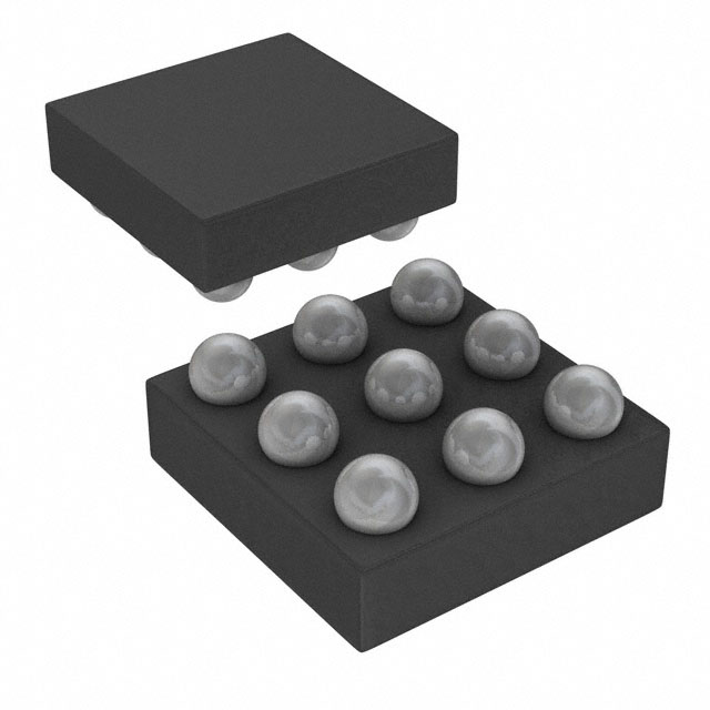
The RT4531 is available in the WL-CSP-9B 1.35x1.35
(BSC) package.
RT4531
Package Type
WSC : WL-CSP-9B 1.35x1.35 (BSC)
Applications
Note :
Smart Phones
Probable Instruments
Backlight for Small and Media Form
Factor LCD Display with Single-cell Battery Input
Richtek products are :
RoHS compliant and compatible with the current requirements of IPC/JEDEC J-STD-020.
Suitable for use in SnPb or Pb-free soldering processes.
Simplified Application Circuit
L
VIN
C1
C3
R1
PWM Dimming
RT4531
EN
PWM
DS4531-01 July 2016
2P10S
WLEDs
IFB1
IFB2
ISET
GND AGND
Copyright © 2016 Richtek Technology Corporation. All rights reserved.
…
Enable
SW
…
VIN
C2
R2
is a registered trademark of Richtek Technology Corporation.
www.richtek.com
1
�RT4531
Pin Configurations
Marking Information
(TOP VIEW)
IFB2
33 : Product Code
ISET
A1
PWM
B1
33W
A2
A3
IFB1
B2
B3
GND
C3
SW
W : Date Code
AGND
C1
C2
VIN
EN
WL-CSP-9B 1.35x1.35 (BSC)
Functional Pin Description
Pin No.
Pin Name
Pin Function
A1
ISET
Full-Scale LED Current Set Pin. Connecting a resistor to the pin programs the
full-scale LED current.
A2
IFB2
Single Output 2 for Backlight LED.
A3
IFB1
Single Output 1 for Backlight LED.
B1
PWM
Enable Control, and PWM Dimming Signal Input.
B2
AGND
Analog Ground.
B3
GND
Power Ground.
C1
EN
Enable Control, and 1-Wire Dimming Signal Input.
C2
VIN
Supply Input Pin.
C3
SW
Switch Node of Boost Converter.
Copyright © 2016 Richtek Technology Corporation. All rights reserved.
www.richtek.com
2
is a registered trademark of Richtek Technology Corporation.
DS4531-01 July 2016
�RT4531
Function Block Diagram
OSC
UVLO
VIN
OTP
OVP
SW
BL
PWM/Drv
DC to DC Core
EN
Control
Logic
PWM
Logic
GND
AGND
OCP
PWM
FB
OVP
ISET
ISET
MINFB
Current Source/
FB Short Detect
IFB1
IFB2
Operation
The RT4531 is a high efficiency solution with 10S2P string
for backlight applications. The RT4531 optimizes the
feedback regulation voltage to provide high efficiency and
also keep high current matching. The RT4531 can receive
either the 1-wire dimming at EN pin or PWM dimming at
PWM pin for brightness dimming. If the 1-wire dimming is
selected, the PWM pin should be kept high; If the PWM
dimming is selected, the EN pin should be kept high.
OCP Protection
The RT4531 features a 1.5A OCP. The driver provides
cycle-by-cycle current limit function to control the current
on power switch. The boost switch turns off when the
inductor current reaches this current threshold and it
remains off until the beginning of the next switching cycle.
This protects the RT4531 and external component under
overload conditions.
OTP Protection
The OTP function will disable boost and current source
when the junction temperature exceeds 150°C. Then
restart to soft-start when the junction temperature is
smaller than 135°C.
Copyright © 2016 Richtek Technology Corporation. All rights reserved.
DS4531-01 July 2016
OVP Protection
The OVP function monitors the SW pin's voltage. Once it
exceeds OVP threshold = 36.5V twice, the boost and
current source will be latched off. Until PWM or EN go
high from low again, the latch state will be released.
1-wire Brightness Dimming
The RT4531 is built-in a 10-bit resolution brightness
control. The EN pin features a simple 1-wire interface to
allow digital brightness control. If the 1-wire dimming is
needed, signals of a specific pattern should be input
detection window into EN pin; Otherwise, PWM pin need
to be enabled.(refer to Timing Diagram1 for Continuous
Coding).The Register Program and register map give an
overview of the protocol used by RT4531.
PWM Brightness Dimming
Besides programmable built-in 1-wire backlight LED
current control, the RT4531 features a built-in PWM
dimming current control by PWM pin, offering a linear
current dimming by external clock source. In order to
guarantee the PWM dimming resolution, recommending
PWM dimming frequency have to be operated at range of
20kHz to 100kHz.
is a registered trademark of Richtek Technology Corporation.
www.richtek.com
3
�RT4531
Absolute Maximum Ratings
(Note 1)
Supply Voltage, VIN ------------------------------------------------------------------------------------------------------LED Switching Voltage, SW -------------------------------------------------------------------------------------------LED Current Source Voltage, IFB1, IFB2 ---------------------------------------------------------------------------Digital Clock Control Pin, EN, PWM --------------------------------------------------------------------------------Other Pins, ISET ---------------------------------------------------------------------------------------------------------Power Dissipation, PD @ TA = 25°C
WL-CSP-9B 1.35x1.35 (BSC) -----------------------------------------------------------------------------------------Package Thermal Resistance (Note 2)
WL-CSP-9B 1.35x1.35 (BSC), θJA -----------------------------------------------------------------------------------Junction Temperature ----------------------------------------------------------------------------------------------------Lead Temperature (Soldering, 10 sec.) ------------------------------------------------------------------------------Storage Temperature Range -------------------------------------------------------------------------------------------ESD Susceptibility (Note 3)
HBM (Human Body Model) ---------------------------------------------------------------------------------------------MM (Machine Model) -----------------------------------------------------------------------------------------------------
Recommended Operating Conditions
−0.3V to 6V
38V
−0.3V to 6V
−0.3V to 6V
−0.3V to 6V
1.22W
81.5°C/W
150°C
260°C
−65°C to 150°C
2kV
200V
(Note 4)
Supply Input Voltage, VIN ------------------------------------------------------------------------------------------------ 2.5V to 5.5V
Junction Temperature Range -------------------------------------------------------------------------------------------- −40°C to 125°C
Ambient Temperature Range -------------------------------------------------------------------------------------------- −40°C to 85°C
Electrical Characteristics
(VIN = 3.6V, CIN = 2.2μF, COUT = 1μF, L = 4.7μH, TA = 25°C, unless otherwise specified)
Parameter
Symbol
Test Conditions
Min
Typ
Max
Unit
Power Supply
UVLO
VUVLO
VIN falls
--
2.2
2.3
V
UVLO Hysteresis Voltage
VUVLO
VIN rises after UVLO
30
50
200
mV
VIN Supply Current
IQ
EN = High, Non-switching
--
1.2
--
mA
VIN Shutdown Current
ISHDN
VIN = 5V
--
1
--
A
Thermal Shutdown
TSD
--
150
--
C
--
15
--
C
IFBx = 20mA
2
--
2
%
IFBx = 20mA
--
1
2
%
IFBx = 500A
IFBx = 20mA, measured on
IFBx pin which has a lower
voltage.
--
1
--
%
200
300
430
mV
0.88
1
1.12
MHz
Thermal Shutdown
Hysteresis
Back Light LED
Accuracy of Back Light
Output Current 1/2
AIBL1, 2
Matching of Output Current
MIBL
BLED Sense Voltage 1/2
VDSBL
Back Light Switching
Frequency
f blosc
Copyright © 2016 Richtek Technology Corporation. All rights reserved.
www.richtek.com
4
is a registered trademark of Richtek Technology Corporation.
DS4531-01 July 2016
�RT4531
Parameter
Symbol
Test Conditions
Min
Typ
Max
Unit
Maximum Duty Cycle
DMAX
90
95
--
%
Back Light N-MOSFET Ron
RDS(ON)_BLN
100
270
400
m
Back Light Current Limit
ILIM_BL
After 5ms in soft-start
1.15
1.5
1.85
A
Back Light Over Voltage
Protection
VBLOVP
Close loop, VIN = 3.6V
35.5
36.5
37.5
V
IFBx Pin Over Voltage
Threshold
VIFBXOVP
Measure on IFBx pin
--
5
--
V
One Wire Detection Delay
tes_delay
300
--
--
s
One Wire Detection Time
tes_det
400
--
--
s
One Wire Detection Window
tes_win
Measure from En low to high
En pin low time in detection
window
Measure from En low to high,
Fblosc = 1MHz
--
1
--
ms
tstart
3
--
--
s
tEOS
3
--
--
s
Logic Control
Start Time of Program
Stream
End Time of Program
Stream
High Time Low Bit
tH_LB
Logic 0
2
--
180
s
Low Time Low Bit
tL_LB
Logic 0
2x
tH_LB
--
360
s
High Time High Bit
tH_HB
Logic 1
2x
tL_HB
--
360
s
Low Time High Bit
tL_HB
Logic 1
2
--
180
s
Logic-Low
VEN_L
--
--
0.4
Logic-High
VEN_H
1.4
--
--
Logic-Low
VPWM_L
--
--
0.4
Logic-High
VPWM_H
1.4
--
--
EN Pull Low Resistor
REN
280
400
520
k
PWM Pull Low Resistor
RPWM
280
400
520
k
PWM Logic Low Width to
Shutdown
TSD_PWM
PWM pin high to low, then
shutdown
20
--
--
ms
EN Logic Low Width to
Shutdown
TDS_EN
EN pin high to low, then
shutdown
2.5
--
--
ms
EN Input
Voltage
PWM Input
Voltage
V
V
Note 1. Stresses beyond those listed “Absolute Maximum Ratings” may cause permanent damage to the device. These are
stress ratings only, and functional operation of the device at these or any other conditions beyond those indicated in
the operational sections of the specifications is not implied. Exposure to absolute maximum rating conditions may
affect device reliability.
Note 2. θJA is measured at TA = 25°C on a high effective thermal conductivity four-layer test board per JEDEC 51-7.
Note 3. Devices are ESD sensitive. Handling precaution is recommended.
Note 4. The device is not guaranteed to function outside its operating conditions.
Copyright © 2016 Richtek Technology Corporation. All rights reserved.
DS4531-01 July 2016
is a registered trademark of Richtek Technology Corporation.
www.richtek.com
5
�RT4531
Typical Application Circuit
L
4.7µH
VIN
2.5V to 5.5V
C1
1µF
R1
10
C3
1µF / 50V
C2
…
…
EN
B1 PWM
PWM Dimming
C3
RT4531
C1
Enable
SW
VIN
C2
1µF
2P10S
WLEDs
A3
IFB1
A2
IFB2
ISET A1
GND AGND
R2
63.4k
B2
B3
Timing Diagram
Timing Diagram1 for 1-wire Continuous Coding
PWM
Tstart
Tes_delay
Tes_det
>300µs
>400µs
Tes_win
Tstart
Addr8 Addr7
=H
=L
D1 = L
EOS
Addr8
=L
3~360µs
2x tL_HB
Programming Code1
Programming Code2
Timing Diagram2 for Shutdown and then Reprogram
PWM
EN
Detection
Window
Programming
Code
Copyright © 2016 Richtek Technology Corporation. All rights reserved.
www.richtek.com
6
> 2.5ms
Shutdown
Detection
Window
Programming
Code
is a registered trademark of Richtek Technology Corporation.
DS4531-01 July 2016
�RT4531
Typical Operating Characteristics
Efficiency vs. Input Voltage
100
95
90
Efficiency(%)
Efficiency (%)
Efficiency vs. Output Current
90
85
80
75
70
65
60
55
50
45
40
35
30
25
20
85
80
ILED = 20mA
ILED = 10mA
75
70
65
60
55
VIN = 3.6V, VOUT = 31V, 10s2p, 20mA/string
VOUT = 31V, 10s2p
50
0
0
0
0.01 0.01 0.01 0.01 0.01 0.02 0.02 0.02
2.5
3
3.5
Output Current (A)
Dimming Linearity
5
5.5
1.3
Switching Frequency (MHz)1
0.020
0.018
Output Current (mA)
4.5
Switching Frequency vs. Input Voltage
0.022
ILED1
ILED2
0.016
0.014
0.012
0.010
0.008
0.006
0.004
0.002
1.2
1.1
1.0
0.9
0.8
VIN = 3.6V
0.000
0.7
0
20
40
60
80
100
2.5
3
3.5
Dimming Duty Cycle (%)
4
4.5
5
5.5
Input Voltage (V)
Switching Frequency vs. Temperature
Sense Voltage vs. Output Current
1.13
0.315
1.08
0.314
Sense Voltage (V)
Switching Frequency (MHz)1
4
Input Voltage(V)
1.03
0.98
0.93
0.313
0.312
0.311
0.88
0.310
-50
-25
0
25
50
75
100
Temperature (°C)
Copyright © 2016 Richtek Technology Corporation. All rights reserved.
DS4531-01 July 2016
125
0
2.5
5
7.5
10
12.5
15
17.5
20
Output Current (mA)
is a registered trademark of Richtek Technology Corporation.
www.richtek.com
7
�RT4531
Application Information
Register Program
1-Wire Interface (Device Address 0x2F)
MSB
LSB MSB
LSB MSB
LSB MSB
Addr Addr Addr Addr Addr Addr Addr Addr
Start
D16 D15 D14 D13 D12 D11 D10
8
7
6
5
4
3
2
1
Address
Data3
Data2
LSB
D9
D8
D7
D6
D5
D4
D3
D2
D1 EOS
Data1
Register Map
Bit
Label
Reset
Description
D16
Ramp Up
0
D15
Ramp Up
0
D14
Ramp Up
1
D13
Ramp Down
0
D12
Ramp Down
0
D11
Ramp Down
1
D10
ILED
0
MSB = sDAC
D9
ILED
0
sDAC
D8
ILED
0
sDAC
D7
ILED
0
sDAC
D6
ILED
0
sDAC
D5
ILED
0
sDAC
D4
ILED
0
sDAC
D3
ILED
0
sDAC
D2
ILED
0
sDAC
D1
ILED
0
LSB = sDAC
[000] = 4s, [001] = 8s, [010] = 16s,[011] = 64s, [100] = 256s,
[101] = 1.024ms, [110] = 2.048ms, [111] = 4.096ms
[000] = 4s, [001] = 8s, [010] = 16s, [011] = 64s, [100] = 256s,
[101] = 1.024ms, [110] = 2.048ms, [111] = 4.096ms
Copyright © 2016 Richtek Technology Corporation. All rights reserved.
www.richtek.com
8
is a registered trademark of Richtek Technology Corporation.
DS4531-01 July 2016
�RT4531
Protection Actions
EN High
Source Current to FBx
Soft-Start/
Normal Operation
N
SW > OVP for
> 8cycles
in 10msec
Y
Latch Off
FBx < 30mV
For 600µs?
N
Soft-Start /Normal
Operation
Y
Y
X = 2?
Latch Off
N
FBx Turned Off
Soft-Start/Normal
Operation
Copyright © 2016 Richtek Technology Corporation. All rights reserved.
DS4531-01 July 2016
is a registered trademark of Richtek Technology Corporation.
www.richtek.com
9
�RT4531
LED Current Setting
The dual channels of the RT4531 can provide up to 20 mA
current each.
No matter either 1-wire Brightness Dimming or PWM
Brightness Dimming is selected, the full-scale current
(current when dimming duty cycle is 100%) of each
channel should be programmed by an external resistor
RISET at ISET pin according to Equation 1.
IFB
V
ISET KISET
RISET
IFBX IFB
DAC code
1024
(2)
Where :
IFB : the full-scale LED current set by the RISET at ISET
pin.
Code : the 10-bit DAC code D1~D10 programmed by 1wire interface.
To enter 1-wire dimming mode, the following digital pattern
on the EN pin must be recognized by the IC when the IC
starts from the shutdown mode.
(1)
Where :
VISET = 1V,
1. Pull the EN pin high to enable the RT4531 and start the
detection window for digital dimming.
KISET = 1268
2. After the digital dimming detection delay time (T -
Brightness Control
es_delay, >300μs), drive the EN low for more than the
detection time (T-es_det, >400μs).
a. 1-wire Brightness Dimming
The RT4531 is built-in a 10-bit resolution brightness
control. The EN pin features a simple 1-wire interface to
allow digital brightness control. If the 1-wire dimming is
needed, signals of a specific pattern should be input
detection window into EN pin; Otherwise, PWM pin need
to be enabled.(refer to Timing Diagram1 for Continuous
Coding).The Register Program and register map give an
overview of the protocol used by RT4531.By the 1-wire
Brightness Dimming, a master can program the 10-bit code
D1(LSB) to D10(MSB) to any of 1024 steps with a single
command. The programmed value will be stored in an
internal register and set the dual-channel current according
to Equation 2. The code will be reset to default value when
the IC is shut down or disabled.
VIN
2.5V to 5.5V
3. Pull the EN pin high after the detection time (>400μs)
and before the detection window (Tes_win,


 工商网监
湘ICP备2023018690号
工商网监
湘ICP备2023018690号