®
RT6276A/B
23V, 6A, 500kHz ACOT® Synchronous Step-Down Converter
General Description
Features
The RT6276A/B is a simple, easy-to-use, 6A synchronous
step-down DC-DC converter with an input supply voltage
range of 4.5V to 23V. The device build-in an accurate 0.6V
reference voltage and integrates low RDS(ON) power
MOSFETs to achieve high efficiency in a UQFN-12HL 3x3
package. The RT6276A/B adopts Advanced Constant OnTime (ACOT®) control architecture to provide an ultrafast
transient response with few external components and to
operate in nearly constant switching frequency over the
line, load, and output voltage range. The RT6276A operates
in automatic PSM that maintains high efficiency during
light load operation. The RT6276B operates in Forced
PWM that helps meet tight voltage regulation accuracy
requirements. The RT6276A/B senses both FETs current
for a robust over-current protection. It features cycle-bycycle current limit protection and prevent the device from
the catastrophic damage in output short circuit, over current
or inductor saturation. A built-in soft-start function prevents
inrush current during start-up. The device also includes
input under-voltage lockout, output under-voltage
protection, over-voltage protection, and over-temperature
protection (thermal shutdown) to provide safe and smooth
operation in all operating conditions. The RT6276A/B is
offered in a UQFN-12HL 3x3(FC) package.
Ω/15mΩ
Ω Low RDS(ON)
6A Converter With Built-In 30mΩ
Power FETs
Input Supply Voltage Range : 4.5V to 23V
Output Voltage Range : 0.6V to 6V
Advanced Constant On-Time (ACOT®) Control
Ultrafast Transient Response
No Needs For External Compensations
Optimized for Low-ESR Ceramic Output Capacitors
0.6V ± 1% High-Accuracy Feedback Reference
Voltage
Optional for Operation Modes :
Power Saving Mode (PSM) (RT6276A)
Forced PWM Mode (RT6276B)
Fixed Switching Frequency : 500kHz
Built-In Internally Fixed Soft-Start (Typ. 0.4ms)
Input Under-Voltage Lockout (UVLO)
Output Under-Voltage Protection (UVP) with Hiccup
Mode
Output Over-Voltage Protection (OVP) with AutoRecovery Mode
Ultrasonic Mode (USM) for RT6276A
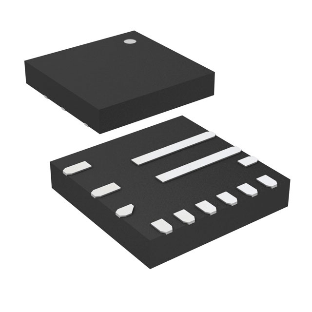
Available In UQFN-12HL 3x3 (FC) (U-Type) Package
Ordering Information
RT6276A/B
Applications
Package Type
QUF : UQFN-12HL 3x3 (FC) (U-Type)
Industrial and Commercial Low Power Systems
Computer Peripherals
LCD Monitors and TVs
Green Electronics/Appliances
Point of Load Regulation for High-Performance DSPs,
FPGAs, and ASICs
Networking Communication
Lead Plating System
G : Green (Halogen Free and Pb Free)
UVP Option
H : Hiccup
PWM Operation Mode
A : Automatic PSM
B: Forced PWM
Note :
Richtek products are :
RoHS compliant and compatible with the current requirements of IPC/JEDEC J-STD-020.
Copyright © 2020 Richtek Technology Corporation. All rights reserved.
DS6276A/B-02 June 2020
Suitable for use in SnPb or Pb-free soldering processes.
is a registered trademark of Richtek Technology Corporation.
www.richtek.com
1
�RT6276A/B
Marking Information
Pin Configuration
RT6276AHGQUF
BOOT
AGND
PGOOD
12 11 10
VCC
FB
BYP
ILMT
(TOP VIEW)
9
8
1
LX
2
NC
3
ME= : Product Code
ME=YM
DNN
YMDNN : Date Code
7
5
EN
VIN
4
PGND
6
RT6276BHGQUF
MD= : Product Code
MD=YM
DNN
UQFN-12HL 3x3
YMDNN : Date Code
Functional Pin Description
Pin No.
Pin Name
Pin Function
1
BOOT
Boot-strap pin. Supply high side gate driver. Decouple this pin to LX pin with
0.1F ceramic cap.
2
LX
Inductor pin. Connect this pin to the switching node of inductor.
3
NC
No internal connection.
4
PGND
Power ground.
5
VIN
Input pin. Decouple this pin to GND pin with at least 10F ceramic cap.
6
EN
Enable control. Pull this pin high to turn on the buck. Do not leave this pin
floating. EN pin will also be used to set USM mode for RT6276A, when EN pin
voltage is between 2.3V and 23V, it will enter USM mode, if EN pin voltage is
between 0.8V and 1.7V, then it is normal mode.
7
PGOOD
Power good Indicator. Open drain output when the output voltage is within 90%
to 120% of regulation point.
8
AGND
Analog ground. Connect AGND to a clean inner GND point with separate trace.
9
VCC
5V linear regulator output for internal control circuit. A capacitor (typical 1F)
should be connected to PGND. Don’t connect to external Load.
10
FB
Output feedback pin. Connect this pin to the center point of the output resistor
divider to program the output voltage.
11
BYP
Bypass input for the internal LDO. BYP is externally connected to the output of
switching regulator. When the BYP voltage rises above the bypass switch
turn-on threshold, the LDO regulator shuts down and the VCC pin is connected
to the BYP pin through an internal switch. But when BYP pin is not used, it
should be connected to ground.
12
ILMT
Current limit setting pin. The current limit is set to 4A, 6A or 8A when this pin is
pull low, floating or pull high respectively.
Copyright © 2020 Richtek Technology Corporation. All rights reserved.
www.richtek.com
2
is a registered trademark of Richtek Technology Corporation.
DS6276A/B-02 June 2020
�RT6276A/B
Functional Block Diagram
VIN
BOOT
Input UVLO
4.2V
LX
ILMT
EN
-
Internal
SST
Thermal
Protection
0.6V
FB
PWM
Control
&
Protect
Logic
+
Current Sense
PGND
PGOOD
AGND
+
EN
4.7V
+
-
VIN
5V
LDO
VCC
BYP
Copyright © 2020 Richtek Technology Corporation. All rights reserved.
DS6276A/B-02 June 2020
is a registered trademark of Richtek Technology Corporation.
www.richtek.com
3
�RT6276A/B
Operation
The RT6276A/B is a high-efficiency, synchronous stepdown DC-DC converter that can deliver up to 6A output
current from a 4.5V to 23V input supply. The RT6276A/B
adopts ACOT®control mode, which can reduce the output
capacitance and provide ultrafast transient responses, and
allow minimal component sizes without any additional
external compensation network.
Input Under-Voltage Lockout
In addition to the EN pin, the RT6276A/B also provides
enable control through the VIN pin. It features an undervoltage lockout (UVLO) function that monitors the internal
linear regulator (VCC). If VEN rises above VENH first,
switching will still be inhibited until the VIN voltage rises
above VUVLO. It is to ensure that the internal regulator is
ready so that operation with not-fully-enhanced internal
MOSFET switches can be prevented. After the device is
powered up, if the input voltage VIN goes below the UVLO
falling threshold voltage (VUVLO − ΔVUVLO), this switching
will be inhibited; if VIN rises above the UVLO rising
threshold (VUVLO), the device will resume switching.
Soft-Start
The soft-start function is used to prevent large inrush
currents while the converter is being powered up. The
RT6276A/B provides an internal soft-start feature for inrush
control. During the start-up sequence, the internal capacitor
is charged by an internal current source ISS to generate a
soft-start ramp voltage as a reference voltage to the PWM
comparator. The device will initiate switching and the
output voltage will smoothly ramp up to its targeted
regulation voltage only after this ramp voltage is greater
than the feedback voltage VFB to ensure the converters
have a smooth start-up. The typical soft-start time is
0.4ms.
Output Over-Voltage Protection (OVP) and UnderVoltage Protection (UVP)
The RT6276A/B includes output under-voltage protection
(UVP) against over-load or short-circuited condition by
constantly monitoring the feedback voltage VFB. If VFB
drops below the under-voltage protection trip threshold
(typically 60% of the internal reference voltage), the UV
comparator will go high to turn off both the internal highside and low-side MOSFET switches.
Power Good
The PGOOD pin is an open-drain output and is connected
to an external pull-up resistor. It is controlled by a
comparator, which the feedback signal VFB is fed to. If
VFB is above 90% of the internal reference voltage, the
PGOOD pin will be in high impedance and VPGOOD will be
held high. Otherwise, the PGOOD output will be pulled
low.
Over-Temperature Protection (Thermal Shutdown)
The RT6276A/B includes an over-temperature protection
(OTP) circuitry to prevent overheating due to excessive
power dissipation. The OTP will shut down switching
operation when junction temperature exceeds a thermal
shutdown threshold TSD. Once the junction temperature
cools down by a thermal shutdown hysteresis (ΔTSD), the
IC will resume normal operation with a complete soft-start.
Over-Current Limit
The RT6276A/B current limit is (4A, 6A, 8A) it is a cycleby-cycle “valley” type, measuring the inductor current
through the synchronous rectifier during the off-time while
the inductor current ramps down. If output voltage drops
below the output under-voltage protection level, the
RT6276A/B will stop switching to avoid excessive heat.
Copyright © 2020 Richtek Technology Corporation. All rights reserved.
www.richtek.com
4
is a registered trademark of Richtek Technology Corporation.
DS6276A/B-02 June 2020
�RT6276A/B
Absolute Maximum Ratings
(Note 1)
Supply Voltage, VIN -------------------------------------------------------------------------------------------Enable Pin Voltage, EN -------------------------------------------------------------------------------------- FB Pin Voltage, FB ------------------------------------------------------------------------------------------- Switch Voltage, LX --------------------------------------------------------------------------------------------33kHz).
Once the internal oscillator is triggered, the controller will
Copyright © 2020 Richtek Technology Corporation. All rights reserved.
www.richtek.com
12
When PGOOD is pulled high and BYP pin of the RT6276A/
B voltage is above 4.7V, an internal 3Ω P-MOSFET switch
connects VCC to the BYP pin while the VCC linear
regulator is simultaneously turned off. Because the VCC
is power source for internal logic device and gate driver. If
bypass function was enabled, it’ s recommended to put a
RC filter to BYP pin to enhance power quality for IC internal
power. But when BYP pin is not used, it should be
connected to ground.
is a registered trademark of Richtek Technology Corporation.
DS6276A/B-02 June 2020
�RT6276A/B
Current Limit
The RT6276A/B current limit is adjustable (4A, 6A, 8A)
by ILMT pin and it is a cycle-by-cycle “valley” type,
measuring the inductor current through the synchronous
rectifier during the off-time while the inductor current ramps
down. The current is determined by measuring the voltage
between source and drain of the synchronous rectifier,
adding temperature compensation for greater accuracy. If
the current exceeds the current limit, the on-time oneshot is inhibited until the inductor current ramps down
below the current limit.
Thus, only when the inductor current is well below the
current limit, another on-time is permitted. If the output
current exceeds the available inductor current (controlled
by the current limit mechanism), the output voltage will
drop. If it drops below the output under-voltage protection
level (see next section) the IC will stop switching to avoid
excessive heat.
Output Over-Voltage Protection and Under-Voltage
Protection
The RT6276A/B include output over-voltage protection
(OVP). If the output voltage rises above the regulation
level, the high-side switch naturally remains off and the
synchronous rectifier will turn on until the inductor current
reaches the zero or next on-time one-shot is triggered If
the output voltage exceeds the OVP threshold for longer
than 20μs (typical), the IC's OVP is triggered. The
RT6276A/B also include output under-voltage protection
(UVP). If the output voltage drops below the UVP trip
threshold for longer than 20μs (typical) the IC's UVP is
triggered. The RT6276A/B use auto-recovery mode in OVP
and Hiccup Mode in UVP. When the UVP function is
triggered remains for a period, the RT6276A/B will retry
automatically. When the UVP condition is removed, the
converter will resume operation. the UVP is disabled during
soft-start period. If the OVP function is triggered, the IC
will stops switching. When the OVP condition is removed,
the converter will resume operation.
Input Under-Voltage Lockout
In addition to the enable function, the RT6276A/B provide
an Under-Voltage Lockout (UVLO) function that monitors
the input voltage. To prevent operation without fullyCopyright © 2020 Richtek Technology Corporation. All rights reserved.
DS6276A/B-02 June 2020
enhanced internal MOSFET switches, this function inhibits
switching when input voltage drops below the UVLO-falling
threshold. The IC resumes switching when input voltage
exceeds the UVLO-rising threshold.
Enable and Disable
The RT6276A/B's EN is used to control converter, the
enable voltage (EN) has a logic-low level of 0.4V. When
VEN is below this level the IC enters shutdown mode When
VEN exceeds its logic-high level of 0.8V the converter is
fully operational.
Soft-Start
The RT6276A/B provide an internal soft-start function to
prevent large inrush current and output voltage overshoot
when the converter starts up. The soft-start (SS)
automatically begins once the chip is enabled. During softstart, it clamps the ramping of internal reference voltage
which is compared with FB signal. The typical soft-start
duration is 0.4ms. A unique PWM duty limit control that
prevents output over-voltage during soft-start period is
designed specifically for FB floating.
Power Good Output (PGOOD)
The power good output is an open drain output that requires
a pull-up resistor. When the output voltage is 15% (typical)
below its set voltage, PGOOD will be pulled low. It is held
low until the output voltage returns to 90% of its set voltage
once more. During soft-start, PGOOD is actively held low
and only allowed to be pulled high after soft-start is over
and the output reaches 90% of its set voltage. There is a
10μs delay built into PGOOD circuitry to prevent false
transition.
External Bootstrap Capacitor (CBOOT)
Connect a 0.1μF low ESR ceramic capacitor between
BOOT pin and LX pin. This bootstrap capacitor provides
the gate driver supply voltage for the high side N-channel
MOSFET switch.
The internal power MOSFET switch gate driver is
optimized to turn the switch on fast enough for low power
loss and good efficiency, but also slow enough to reduce
EMI. Switch turn-on is when most EMI occurs since VLX
rises rapidly. In some cases, it is desirable to reduce EMI
is a registered trademark of Richtek Technology Corporation.
www.richtek.com
13
�RT6276A/B
further, by the expense of some additional power
dissipation. The switch turn-on can be slowed by placing
a small (10Ω ≤ RBOOT ≤ 30Ω) resistance between BOOT
and the external bootstrap capacitor. This will slow the
high-side switch turn-on and VLX's rise. In order to improve
EMI performance and enhancement of the internal
MOSFET switch.
Output Voltage Setting
Set the desired output voltage using a resistive divider
from the output to ground with the midpoint connected to
FB. The output voltage is set according to the following
equation:
VOUT,VALLEY = 1+ R1 0.6V
R2
VOUT
R1
FB
RT6276A/B
R2
GND
Figure 2. Output Voltage Setting
Place the FB resistors within 5mm of the FB pin. Choose
R2 between 10kΩ and 100kΩ to minimize power
consumption without excessive noise pick-up and
calculate R1 as follows :
R1 =
R2 x (VOUT 0.6V)
0.6V
For output voltage accuracy, use divider resistors with 1%
or better tolerance.
Inductor Selection
Selecting an inductor involves specifying its inductance
and also its required peak current. The exact inductor value
is generally flexible and is ultimately chosen to obtain the
best mix of cost, physical size, and circuit efficiency.
Lower inductor values benefit from reduced size and cost
and they can improve the circuit’s transient response,
but they increase the inductor ripple current and output
voltage ripple and reduce the efficiency due to the resulting
higher peak currents. Conversely, higher inductor values
increase efficiency, but the inductor will either be physically
larger or have higher resistance since more turns of wire
are required and transient response will be slower since
Copyright © 2020 Richtek Technology Corporation. All rights reserved.
www.richtek.com
14
more time is required to change current (up or down) in
the inductor. A good compromise between size, efficiency,
and transient response is to use a ripple current (ΔIL) about
20-50% of the desired full output load current. Calculate
the approximate inductor value by selecting the input and
output voltages, the switching frequency (f SW), the
maximum output current (IOUT(MAX)) and estimating a ΔIL
as some percentage of that current.
V
(VIN VOUT )
L OUT
VIN fSW IL
Once an inductor value is chosen, the ripple current (ΔIL)
is calculated to determine the required peak inductor
current.
VOUT (VIN VOUT )
and
VIN fSW L
I
IL(PEAK) IOUT(MAX) L
2
To guarantee the required output current, the inductor
needs a saturation current rating and a thermal rating that
exceeds IL(PEAK). These are minimum requirements. To
maintain control of inductor current in overload and shortcircuit conditions, some applications may desire current
ratings up to the current limit value. However, the IC's
output under-voltage shutdown feature make this
unnecessary for most applications.
IL
For best efficiency, choose an inductor with a low DC
resistance that meets the cost and size requirements.
For low inductor core losses some type of ferrite core is
usually best and a shielded core type, although possibly
larger or more expensive, will probably give fewer EMI
and other noise problems.
Input Capacitor Selection
High quality ceramic input decoupling capacitor, such as
X5R or X7R, with values greater than 20μF are
recommended for the input capacitor. The X5R and X7R
ceramic capacitors are usually selected for power regulator
capacitors because the dielectric material has less
capacitance variation and more temperature stability.
Voltage rating and current rating are the key parameters
when selecting an input capacitor. Generally, selecting an
input capacitor with voltage rating 1.5 times greater than
the maximum input voltage is a conservatively safe design.
The input capacitor is used to supply the input RMS
is a registered trademark of Richtek Technology Corporation.
DS6276A/B-02 June 2020
�RT6276A/B
current, which can be calculated using the following
equation :
IRMS
VOUT
V
I 2
(1 OUT ) IOUT 2 L
VIN
VIN
12
The next step is to select a proper capacitor for RMS
current rating. One good design uses more than one
capacitor with low Equivalent Series Resistance (ESR) in
parallel to form a capacitor bank. The input capacitance
value determines the input ripple voltage of the regulator.
The input voltage ripple can be approximately calculated
using the following equation :
VIN
IOUT VIN
V
(1 OUT )
CIN fSW VOUT
VIN
The typical operating circuit is recommended to use two
10μF low ESR ceramic capacitors on the input.
Output Capacitor Selection
The IC is optimized for ceramic output capacitors and best
performance will be obtained by using them. The total
output capacitance value is usually determined by the
desired output voltage ripple level and transient response
requirements for sag (undershoot on positive load steps)
and soar (overshoot on negative load steps).
Output ripple at the switching frequency is caused by the
inductor current ripple and its effect on the output
capacitor's ESR and stored charge. These two ripple
components are called ESR ripple and capacitive ripple.
Since ceramic capacitors have extremely low ESR and
relatively little capacitance, both components are similar
in amplitude and both should be considered if ripple is
critical.
VRIPPLE VRIPPLE(ESR) VRIPPLE(C)
VRIPPLE(ESR) IL RESR
VRIPPLE(C)
IL
8 COUT fSW
In addition to voltage ripple at the switching frequency,
the output capacitor and its ESR also affect the voltage
sag (undershoot) and soar (overshoot) when the load steps
up and down abruptly. The ACOT® transient response is
very quick and output transients are usually small.
However, the combination of small ceramic output
capacitors (with little capacitance), low output voltages
(with little stored charge in the output capacitors), and
Copyright © 2020 Richtek Technology Corporation. All rights reserved.
DS6276A/B-02 June 2020
low duty cycle applications (which require high inductance
to get reasonable ripple currents with high input voltages)
increases the size of voltage variations in response to
very quick load changes. Typically, load changes occur
slowly with respect to the IC's switching frequency.
However, some modern digital loads can exhibit nearly
instantaneous load changes and the following section
shows how to calculate the worst-case voltage swings in
response to very fast load steps.
The amplitude of the ESR step up or down is a function of
the load step and the ESR of the output capacitor :
VESR_STEP IOUT RESR
The amplitude of the capacitive sag is a function of the
load step, the output capacitor value, the inductor value,
the input-to-output voltage differential, and the maximum
duty cycle. The maximum duty cycle during a fast transient
is a function of the on-time and the minimum off-time since
the ACOT® control scheme will ramp the current using
on-times spaced apart with minimum off-times, which is
as fast as allowed. Calculate the approximate on-time
(neglecting parasitics) and maximum duty cycle for a given
input and output voltage as :
VOUT
tON
tON
and DMAX
VIN fSW
tON + tOFF_MIN
The actual on-time will be slightly longer as the IC
compensates for voltage drops in the circuit, but we can
neglect both of these since the on-time increases
compensations for the voltage losses. Calculate the output
voltage SAG as :
VSAG
L (IOUT )2
2 COUT ( VIN(MIN) DMAX VOUT )
The amplitude of the capacitive SOAR is a function of the
load step, the output capacitor value, the inductor value
and the output voltage :
VSOAR
L ( IOUT )2
2 COUT VOUT
Most applications never experience instantaneous full load
steps and the IC's high switching frequency and fast
transient response can easily control voltage regulation
at all times. Therefore, sag and soar are seldom an issue
except in very low-voltage CPU core or DDR memory
supply applications, particularly for devices with high clock
frequencies and quick changes into and out of sleep
is a registered trademark of Richtek Technology Corporation.
www.richtek.com
15
�RT6276A/B
In any application with large quick transients, it should
calculate soar and sag to make sure that over-voltage
protection and under-voltage protection will not be triggered.
Thermal Considerations
The junction temperature should never exceed the
absolute maximum junction temperature TJ(MAX), listed
under Absolute Maximum Ratings, to avoid permanent
damage to the device. The maximum allowable power
dissipation depends on the thermal resistance of the IC
package, the PCB layout, the rate of surrounding airflow,
and the difference between the junction and ambient
temperatures. The maximum power dissipation can be
calculated using the following formula :
4.0
Maximum Power Dissipation (W)1
modes. In such applications, simply increasing the amount
of ceramic output capacitor (sag and soar are directly
proportional to capacitance) or adding extra bulk
capacitance can easily eliminate any excessive voltage
transients.
Four-Layer PCB
3.5
3.0
2.5
2.0
1.5
1.0
0.5
0.0
0
25
50
75
100
125
Ambient Temperature (°C)
Figure 3. Derating Curve of Maximum Power Dissipation
PD(MAX) = (TJ(MAX) − TA) / θJA
where TJ(MAX) is the maximum junction temperature, TA is
the ambient temperature, and θJA is the junction-to-ambient
thermal resistance.
For continuous operation, the maximum operating junction
temperature indicated under Recommended Operating
Conditions is 125°C. The junction-to-ambient thermal
resistance, θJA, is highly package dependent. For a UQFN12HL 3x3 (FC) package, the thermal resistance, θJA, is
38.4°C/W on a standard JEDEC 51-7 high effective-thermalconductivity four-layer test board. The maximum power
dissipation at TA = 25°C can be calculated as below :
PD(MAX) = (125°C − 25°C) / (38.4°C/W) = 2.6W for a
UQFN-12HL 3x3 (FC) package.
The maximum power dissipation depends on the operating
ambient temperature for the fixed TJ(MAX) and the thermal
resistance, θJA. The derating curves in Figure 3 allows
the designer to see the effect of rising ambient temperature
on the maximum power dissipation.
Copyright © 2020 Richtek Technology Corporation. All rights reserved.
www.richtek.com
16
is a registered trademark of Richtek Technology Corporation.
DS6276A/B-02 June 2020
�RT6276A/B
Layout Considerations
AGND
VOUT
Put the input capacitor as close as possible to the device
pins (VIN and GND).
The LX node encounters high frequency voltage swings
so it should be kept in a small area. Keep sensitive
components away from the LX node to prevent stray as
possible.
The GND pin should be connected to a strong ground
plane for heat sinking and noise protection.
Avoid using vias in the power path connections that have
switched currents (from CIN to GND and CIN to VIN) and
the switching node (LX).
L
COUT
LX
NC
FB
BYP
12 11 10
AGND
PGOOD
Make traces of the high current paths as short and wide
as possible.
LX should be connected to
inductor by wide and short
trace.
Keep sensitive components
away from this trace. BOOT
VCC
R2
The optional compensation
Compensation components
must be connected as close
CFF (opt.)
GND
to the IC as possible.
CBYS
CVCC
GND
VVCC
ILMT
Layout is very important in high frequency switching
converter design. The PCB can radiate excessive noise
and contribute to converter instability with improper layout.
Certain points must be considered before starting a layout
using the IC.
R1
9
8
1
7
The input capacitor
must be placed as
close to the IC as
possible
5
EN
VIN
4
PGND
6
VIN
2
CIN
3
The output capacitor must
be placed near the IC
GND
Figure 4. PCB Layout Guide
An example of PCB layout guide is shown in Figure 4 for
reference.
Copyright © 2020 Richtek Technology Corporation. All rights reserved.
DS6276A/B-02 June 2020
is a registered trademark of Richtek Technology Corporation.
www.richtek.com
17
�RT6276A/B
Outline Dimension
Symbol
Dimensions In Millimeters
Dimensions In Inches
Min
Max
Min
Max
A
0.500
0.600
0.020
0.024
A1
0.000
0.050
0.000
0.002
A3
0.100
0.200
0.004
0.008
D
2.900
3.100
0.114
0.122
E
2.900
3.100
0.114
0.122
b
0.100
0.200
0.004
0.008
b1
0.180
0.280
0.007
0.011
L
0.800
1.000
0.031
0.039
L1
1.730
1.930
0.068
0.076
L2
0.250
0.450
0.010
0.018
e
0.720
0.028
e1
0.900
0.035
e2
0.450
0.018
K
0.500
0.020
K1
0.950
0.037
U-Type 12HL QFN 3x3 (FC) Package
Copyright © 2020 Richtek Technology Corporation. All rights reserved.
www.richtek.com
18
is a registered trademark of Richtek Technology Corporation.
DS6276A/B-02 June 2020
�RT6276A/B
Footprint Information
Package
Number
of Pin
UQFN3*312H(FC)
12
Footprint Dimension (mm)
P
P1
P2
Ax
C*8
C1*2 C2*2 D*12
K
K1
K2
K3
0.450 0.720 0.900 3.800 0.800 1.350 2.280 0.230 0.619 0.169 1.100 1.900
Tolerance
±0.050
Richtek Technology Corporation
14F, No. 8, Tai Yuen 1st Street, Chupei City
Hsinchu, Taiwan, R.O.C.
Tel: (8863)5526789
Richtek products are sold by description only. Richtek reserves the right to change the circuitry and/or specifications without notice at any time. Customers should
obtain the latest relevant information and data sheets before placing orders and should verify that such information is current and complete. Richtek cannot
assume responsibility for use of any circuitry other than circuitry entirely embodied in a Richtek product. Information furnished by Richtek is believed to be
accurate and reliable. However, no responsibility is assumed by Richtek or its subsidiaries for its use; nor for any infringements of patents or other rights of third
parties which may result from its use. No license is granted by implication or otherwise under any patent or patent rights of Richtek or its subsidiaries.
DS6276A/B-02 June 2020
www.richtek.com
19
�


 工商网监
湘ICP备2023018690号
工商网监
湘ICP备2023018690号
