®
RT7262A
2A, 21V 500kHz Synchronous Step-Down Converter
General Description
Features
The RT7262A is a synchronous step-down regulator with
integrated power MOSFETs. It achieves 2A of continuous
output current over a wide input supply range with excellent
load and line regulation. Current mode operation provides
fast transient response and eases loop stabilization.
z
Wide Input Range : 4.5V to 21V
Adjustable Output from 0.808V to 15V
z 2A Output Current
z 150mΩ
Ω/60mΩ
Ω Internal Power MOSFET Switch
z Internal Compensation Minimizes External Parts
z 500kHz Fixed Switching Frequency
z Synchronized External Clock from 300kHz to 2MHz
z Adjustable Soft-Start
z Cycle-by-Cycle Over Current Limit
z Thermal Shutdown Protection
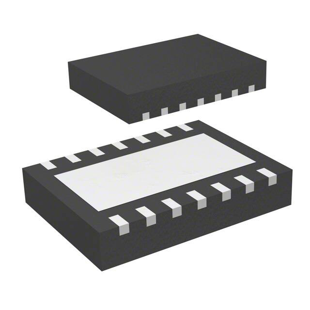
z Available in SOP-8 (Exposed Pad) and WDFN-14L
4x3 Packages
z RoHS Compliant and Halogen Free
z
Fault condition protection includes cycle-by-cycle current
limiting and thermal shutdown. An adjustable soft-start
reduces the stress on the input source at start-up.
The RT7262A requires a minimal number of readily
available external components, providing a compact
solution.
Ordering Information
RT7262A
Applications
Package Type
QW : WDFN-14L 4x3 (W-Type)
SP : SOP-8 (Exposed Pad-Option 2)
Lead Plating System
Z : ECO (Ecological Element with
Halogen Free and Pb free)
z
z
z
z
Distributive Power Systems
Battery Charger
DSL Modems
Pre-Regulator for Linear Regulators
Note :
Richtek products are :
`
RoHS compliant and compatible with the current requirements of IPC/JEDEC J-STD-020.
`
Suitable for use in SnPb or Pb-free soldering processes.
Simplified Application Circuit
VIN
BOOT
VIN
EN/SYNC
VCC
CC
Copyright © 2012 Richtek Technology Corporation. All rights reserved.
September 2012
L
SW
Chip Enable
DS7262A-01
CBOOT
RT7262A
CIN
FB
GND
VOUT
RT
R1
R2
COUT
is a registered trademark of Richtek Technology Corporation.
www.richtek.com
1
�RT7262A
Marking Information
Pin Configurations
RT7262AZQW
(TOP VIEW)
07 : Product Code
VIN
SW
SW
SW
SW
BOOT
EN/SYNC
YMDNN : Date Code
07 YM
DNN
RT7262AZSP
YMDNN : Date Code
2
3
4
5
6
12
11
10
9
GND
15
7
8
AGND
GND
GND
VCC
SS
PGOOD
FB
WDFN-14L 4x3
RT7262AZSP : Product Number
RT7262A
ZSPYMDNN
14
13
1
VIN
8
SW
2
SW
3
BOOT
4
GND
GND
7
VCC
6
FB
5
EN/SYNC
9
SOP-8 (Exposed Pad)
Functional Pin Description
Pin No.
WDFN-14L 4x3
1
SOP-8
(Exposed Pad)
1
2, 3, 4, 5
2, 3
6
4
Pin Name
Pin Function
VIN
Power Input. VIN supplies the power to the IC, as well as the
step-down converter switches. Drive VIN with a 4.5V to 21V
power source. Bypass VIN to GND with a suitably large
capacitor to eliminate noise on the input to the IC.
SW
Switch Node. SW is the switching node that supplies power to
the output. Connect the output LC filter from SW to the output
load. Note that a capacitor is required from SW to BOOT to
power the high side switch.
BOOT
Bootstrap for High Side Gate Driver. Connect a 100nF or greater
capacitor from SW to BOOT to power the high side switch driver.
7
5
EN/SYNC
Enable or External Frequency Synchronization Input. For
automatic start-up, connect the EN/SYNC pin to VIN with a
100kΩ resistor. The switching frequency can be changed by an
external clock applying to the SYNC pin.
8
6
FB
Feedback Input. FB senses the output voltage via an external
resistive voltage divider. The feedback reference voltage is
0.808V typically.
9
--
PGOOD
Power Good Indicator is an Open Drain Output. The power good
rising/falling threshold is 90%/70% of regulation output voltage.
10
--
SS
Soft-Start Control Input. Connect a capacitor from SS to GND to
set the soft-start period.
11
7
VCC
Bias Supply. Decouple with 0.1μF to 0.22μF capacitor between
this pin and GND.
12, 13, 15
8,
GND
(Exposed Pad) 9 (Exposed Pad)
Ground. The exposed pad must be soldered to a large PCB and
connected to GND for maximum power dissipation.
14
--
AGND
Copyright © 2012 Richtek Technology Corporation. All rights reserved.
www.richtek.com
2
Analog Ground. Connect this pin to the system ground in PCB
layout.
is a registered trademark of Richtek Technology Corporation.
DS7262A-01
September 2012
�RT7262A
Function Block Diagram
For WDFN-14L 4x3 Package
VIN
Shutdown
Comparator
1.2V
+
-
Regulator
VA
VA
VC
5k
EN/SYNC
Current Sense
Amplifier
+
Ramp
Generator
Oscillator
S
-
1µA
Q
+
3V
1.7V
BOOT
+
Lockout
Comparator
VCC
PGOOD
Driver
R
PWM
Comparator
SW
Reference
+
Error
+ Amplifier
+
-
-
FB
VC
30pF
GND
400k
10µA
SS
1pF
For SOP-8 (Exposed Pad) Package
VIN
1.2V
EN/SYNC
Shutdown
Comparator
+
Regulator
-
Current Sense
Amplifier
+
Ramp
Generator
BOOT
S
Oscillator
5k
Q
-
1µA
3V
1.7V
+
+
Lockout
Comparator
VCC
Reference
FB
PWM
Comparator
Error
+ Amplifier
Driver
R
SW
GND
-
30pF
400k
1pF
Copyright © 2012 Richtek Technology Corporation. All rights reserved.
DS7262A-01
September 2012
is a registered trademark of Richtek Technology Corporation.
www.richtek.com
3
�RT7262A
Operation
The RT7262A is a constant frequency, current mode
synchronous step-down converter. In normal operation,
the high side N-MOSFET is turned on when the S-R latch
is set by the oscillator and is turned off when the current
comparator resets the S-R latch. While the high side
N-MOSFET is turned off, the low side N-MOSFET is turned
on to conduct the inductor current until next cycle begins.
Error Amplifier
The error amplifier adjusts its output voltage by comparing
the feedback signal (VFB) with the internal reference. When
the load current increases, it causes a drop in the feedback
voltage relative to the reference, the error amplifier's output
voltage then rises to allow higher inductor current to match
the load current.
Oscillator
The internal oscillator runs at fixed frequency 500kHz. In
short circuit condition, the frequency is reduced to 150kHz
for low power consumption.
Soft-Start (SS)
An internal current source charges an internal capacitor
to build a soft-start ramp voltage. The FB voltage will track
the internal ramp voltage during soft-start interval. The
typical soft-start time is 4ms.
UV Comparator
If the feedback voltage (VFB) is lower than 0.4V, the UV
Comparator will go high to turn off the high side MOSFET.
The output under voltage protection is designed to operate
in Hiccup mode. When the UV condition is removed, the
converter will resume switching.
Thermal Shutdown
The over temperature protection function will shut down
the switching operation when the junction temperature
exceeds 150°C. Once the junction temperature cools
down by approximately 30°C, the converter will
automatically resume switching.
Internal Regulator
The regulator provides low voltage power to supply the
internal control circuits and the bootstrap power for high
side gate driver.
Enable
The converter is turned on when the EN pin is higher than
2V. When the EN pin is lower than 0.4V, the converter will
enter shutdown mode and reduce the supply current to
be less than 1μA.
Copyright © 2012 Richtek Technology Corporation. All rights reserved.
www.richtek.com
4
is a registered trademark of Richtek Technology Corporation.
DS7262A-01
September 2012
�RT7262A
Absolute Maximum Ratings
z
z
z
z
z
z
z
z
z
z
(Note 1)
Supply Voltage, VIN ------------------------------------------------------------------------------------------Switch Voltage, SW ------------------------------------------------------------------------------------------Boot Voltage, BOOT ------------------------------------------------------------------------------------------Other Pins -------------------------------------------------------------------------------------------------------Power Dissipation, PD @ TA = 25°C
WDFN-14L 4x3 -------------------------------------------------------------------------------------------------SOP-8 (Exposed Pad) ---------------------------------------------------------------------------------------Package Thermal Resistance (Note 2)
WDFN-14L 4x3, θJA -------------------------------------------------------------------------------------------WDFN-14L 4x3, θJC -------------------------------------------------------------------------------------------SOP-8 (Exposed Pad), θJA ----------------------------------------------------------------------------------SOP-8 (Exposed Pad), θJC ---------------------------------------------------------------------------------Junction Temperature -----------------------------------------------------------------------------------------Lead Temperature (Soldering, 10 sec.) -------------------------------------------------------------------Storage Temperature Range --------------------------------------------------------------------------------ESD Susceptibility (Note 3)
HBM (Human Body Model) -----------------------------------------------------------------------------------
Recommended Operating Conditions
z
z
z
−0.3V to 26V
−0.3V to (VIN + 0.3V)
(SW − 0.3V) to (SW + 6V)
−0.3V to 6V
1.667W
1.333W
60°C/W
7.5°C/W
75°C/W
15°C/W
150°C
260°C
−65°C to 150°C
2kV
(Note 4)
Supply Input Voltage Range, VIN --------------------------------------------------------------------------- 4.5V to 21V
Junction Temperature Range --------------------------------------------------------------------------------- −40°C to 125°C
Ambient Temperature Range --------------------------------------------------------------------------------- −40°C to 85°C
Electrical Characteristics
(VIN = 12V, TA = 25°C, unless otherwise specified)
Parameter
Symbol
Test Conditions
Min
Typ
Max
Unit
Shutdown Current
ISHDN
VEN = 0
--
0
1
μA
Quiescent Current
IQ
VEN = 2V, VFB = 1V
--
0.7
--
mA
Upper Switch On Resistance
R DS(ON)1
--
150
--
mΩ
Lower Switch On Resistance
R DS(ON)2
--
60
--
mΩ
Switch Leakage
ILEAK
VEN = 0V, VSW = 0V or 12V
--
0
10
μA
Current Limit
ILIM
VBOOT − VSW = 4.8V
3.9
5.5
--
A
Oscillator Frequency
f SW
VFB = 0.75V
425
500
575
kHz
Logic-High
VSYNCH
1.8
--
--
Logic-Low
VSYNCL
--
--
0.4
0.3
--
2
MHz
--
1.5
2.5
μA
Power Good Rising Threshold
--
90
--
%
Power Good Falling Threshold
--
70
--
%
--
--
0.4
V
SYNC Threshold
Voltage
SYNC Frequency Range
f SYNC
SYNC Input Current
ISYNC
Power Good Sink Current
Capability
Copyright © 2012 Richtek Technology Corporation. All rights reserved.
DS7262A-01
September 2012
VSYNC = 6V
Sink 4mA
V
is a registered trademark of Richtek Technology Corporation.
www.richtek.com
5
�RT7262A
Parameter
Symbol
Test Conditions
Min
Typ
Max
Unit
--
10
--
nA
VFB = 0V
--
150
--
kHz
VFB = 0.8V
--
90
--
%
--
100
--
ns
0.796
0.808
0.82
V
nA
Power Good Leakage Current
Short Circuit Frequency
Maximum Duty Cycle
D MAX
Minimum On Time
tON
Feedback Voltage
VFB
Feedback Current
IFB
--
10
50
Logic-High
VIH
2
--
5.5
Logic-Low
VIL
--
--
0.4
VEN = 2V
--
1
--
VEN = 0V
--
0
--
VIN Rising
3.8
4
4.2
V
--
400
--
mV
--
5
--
V
ICC = 5mA
--
5
--
%
CSS = 47nF
--
4.7
--
ms
EN Voltage
EN Current
IEN
Under Voltage Lockout Threshold
Under Voltage Lockout Threshold
Hysteresis
VCC Regulator
VUVLO
4.5V ≤ VIN ≤ 21V
ΔVUVLO
VCC Load Regulation
Soft-Start Period
tSS
Thermal Shutdown Threshold
TSD
--
150
--
Thermal Shutdown Hysteresis
ΔTSD
--
30
--
V
μA
°C
Note 1. Stresses beyond those listed “Absolute Maximum Ratings” may cause permanent damage to the device. These are
stress ratings only, and functional operation of the device at these or any other conditions beyond those indicated in
the operational sections of the specifications is not implied. Exposure to absolute maximum rating conditions may
affect device reliability.
Note 2. θJA is measured at TA = 25°C on a high effective thermal conductivity four-layer test board per JEDEC 51-7. θJC is
measured at the exposed pad of the package.
Note 3. Devices are ESD sensitive. Handling precaution is recommended.
Note 4. The device is not guaranteed to function outside its operating conditions.
Copyright © 2012 Richtek Technology Corporation. All rights reserved.
www.richtek.com
6
is a registered trademark of Richtek Technology Corporation.
DS7262A-01
September 2012
�RT7262A
Typical Application Circuit
For WDFN-14L 4x3 Package
1
VIN
BOOT
VIN
CIN
22µF
RT7262A
SW
6
CBOOT
100nF
2, 3, 4, 5
L
VOUT
9 PGOOD
PGOOD
R3
100k
11
R1
RT
FB 8
VCC
CC
0.1µF
COUT
CSS
47nF
SS 10
R2
7 EN/SYNC
ON/OFF
AGND GND
14
12, 13, 15 (Exposed Pad)
For SOP-8 (Exposed Pad) Package
1
VIN
CIN
22µF
Chip Enable
BOOT
VIN
4
CBOOT
100nF
RT7262A
SW
5 EN/SYNC
8, 9 (Exposed Pad)
GND
2, 3
L
VOUT
6
FB
RT
VCC 7
R2
R1
COUT
CC
0.1µF
Table 1. Recommended Components Selection
VOUT (V)
R1 (kΩ)
R2 (kΩ)
RT (kΩ)
L (μH)
COUT (μF)
5
75
14.46
0
4.7
22 x 2
3.3
75
24.32
0
3.6
22 x 2
2.5
75
35.82
0
3.6
22 x 2
1.8
5
4.07
30
2
22 x 2
1.5
5
5.84
39
2
22 x 2
1.2
5
10.31
47
2
22 x 2
1.05
5
16.69
47
1.5
22 x 2
Copyright © 2012 Richtek Technology Corporation. All rights reserved.
DS7262A-01
September 2012
is a registered trademark of Richtek Technology Corporation.
www.richtek.com
7
�RT7262A
Typical Operating Characteristics
Efficiency vs. Output Current
Reference Voltage vs. Input Voltage
100
0.825
90
0.820
70
Reference Voltage (V)
Efficiency (%)
80
VIN = 12V
VIN = 21V
60
50
40
30
20
0.815
0.810
0.805
0.800
0.795
0.790
10
VOUT = 1.22V, IOUT = 0A to 2A
0
0.785
0
0.25
0.5
0.75
1
1.25
1.5
1.75
2
4
6
8
10
14
16
18
20
22
Input Voltage (V)
Output Current (A)
Output Voltage vs. Output Current
Reference Voltage vs. Temperature
0.84
1.26
0.83
1.25
0.82
1.24
Output Voltage (V)
Reference Voltage (V)
12
0.81
0.80
0.79
0.78
1.23
1.22
VIN = 21V
VIN = 12V
1.21
1.20
0.77
1.19
0.76
1.18
VOUT = 1.22V, IOUT = 0A to 2A
-50
-25
0
25
50
75
100
125
0
0.25
0.5
Temperature (°C)
Switching Frequency vs. Input Voltage
1
1.25
1.5
1.75
2
Switching Frequency vs. Temperature
550
650
Switching Frequency (kHz)1
Switching Frequency (kHz)1
0.75
Output Current (A)
525
500
475
450
425
600
550
500
450
400
350
VOUT = 1.22V
VIN = 12V, VOUT = 1.22V
400
300
4
6
8
10
12
14
16
18
20
Input Voltage (V)
Copyright © 2012 Richtek Technology Corporation. All rights reserved.
www.richtek.com
8
22
-50
-25
0
25
50
75
100
125
Temperature (°C)
is a registered trademark of Richtek Technology Corporation.
DS7262A-01
September 2012
�RT7262A
Current Limit vs. Temperature
10
8
8
Current Limit (A)
Current Limit (A)
Current Limit vs. Input Voltage
10
6
4
6
4
2
2
0
0
VIN = 12V, VOUT = 1.22V
4
6
8
10
12
14
16
18
20
22
-50
0
25
50
75
100
Input Voltage (V)
Temperature (°C)
Load Transient Response
Load Transient Response
VOUT
(200mV/Div)
VOUT
(100mV/Div)
IOUT
(1A/Div)
IOUT
(1A/Div)
VIN = 12V, VOUT = 1.22V, IOUT = 0A to 2A
Time (100μs/Div)
Output Ripple Voltage
Output Ripple Voltage
VOUT
(50mV/Div)
VSW
(10V/Div)
VSW
(10V/Div)
IL
(1A/Div)
IL
(2A/Div)
VIN = 12V, IOUT = 1A
Time (1μs/Div)
Copyright © 2012 Richtek Technology Corporation. All rights reserved.
September 2012
125
VIN = 12V, VOUT = 1.22V, IOUT = 1A to 2A
Time (100μs/Div)
VOUT
(50mV/Div)
DS7262A-01
-25
VIN = 12V, IOUT = 2A
Time (1μs/Div)
is a registered trademark of Richtek Technology Corporation.
www.richtek.com
9
�RT7262A
Power Off from VIN
Power On from VIN
VIN
(10V/Div)
VIN
(10V/Div)
VOUT
(1V/Div)
VOUT
(1V/Div)
VPGOOD
(5V/Div)
IL
(5A/Div)
VPGOOD
(5V/Div)
IL
(5A/Div)
VIN = 12V, VOUT = 1.22V, IOUT = 2A
Time (5ms/Div)
Time (25ms/Div)
Power On from EN
Power Off from EN
VEN
(5V/Div)
VEN
(5V/Div)
VOUT
(1V/Div)
VOUT
(1V/Div)
VPGOOD
(5V/Div)
IL
(5A/Div)
VPGOOD
(5V/Div)
IL
(5A/Div)
VIN = 12V, VOUT = 1.22V, IOUT = 2A
Time (2.5ms/Div)
Copyright © 2012 Richtek Technology Corporation. All rights reserved.
www.richtek.com
10
VIN = 12V, VOUT = 1.22V, IOUT = 2A
VIN = 12V, VOUT = 1.22V, IOUT = 2A
Time (50μs/Div)
is a registered trademark of Richtek Technology Corporation.
DS7262A-01
September 2012
�RT7262A
Application Information
The IC is a synchronous high voltage step-down converter
that can support the input voltage range from 4.5V to 21V
and the output current can be up to 2A.
Output Voltage Setting
The output voltage is set by an external resistive divider
according to the following equation :
VOUT = VFB ⎛⎜ 1+ R1 ⎞⎟
⎝ R2 ⎠
where VFB is the feedback reference voltage 0.808V
(typical).
The resistive divider allows the FB pin to sense a fraction
of the output voltage as shown in Figure 1.
VOUT
R1
FB
RT7262A
R2
GND
Figure 1. Output Voltage Setting
Soft-Start for WDFN-14L Package
The RT7262AZQW (WDFN-14L package) contains an
external soft-start clamp that gradually raises the output
voltage. The soft-start timing is programmed by the
external capacitor between SS pin and GND. The chip
provides an internal 10μA charge current for the external
capacitor. If 47nF capacitor is used to set the soft-start,
the period will be 4.7ms (typ.).
Soft-Start for SOP-8 (Exposed Pad) Package
The RT7262AZSP (SOP-8 (Exposed Pad) package)
contains an internal soft-start function to prevent large
inrush current and output voltage overshoot when the
converter starts up. Soft-start automatically begins once
the chip is enabled. During soft-start, the internal softstart capacitor becomes charged and generates a linear
ramping up voltage across the capacitor. This voltage
clamps the voltage at the internal reference, causing the
duty pulse width to increase slowly and in turn reduce the
output surge current. The typical soft-start time for this
IC is set at 2ms.
External Bootstrap Diode
Under Voltage Lockout Threshold
Connect a 100nF low ESR ceramic capacitor between
the BOOT pin and SW pin as shown in Figure 2. This
capacitor provides the gate driver voltage for the high side
MOSFET. It is recommended to add an external bootstrap
diode between an external 5V and BOOT pin for efficiency
improvement when input voltage is lower than 5.5V or duty
ratio is higher than 65% .The bootstrap diode can be a
low cost one such as IN4148 or BAT54. The external 5V
can be a 5V fixed input from system or a 5V output of the
IC. Note that the external boot voltage must be lower than
5.5V.
The IC includes an input Under Voltage Lockout Protection
(UVLO). If the input voltage exceeds the UVLO rising
threshold voltage (4.2V), the converter resets and prepares
the PWM for operation. If the input voltage falls below the
UVLO falling threshold voltage (3.8V) during normal
operation, the device stops switching. The UVLO rising
and falling threshold voltage includes a hysteresis to
prevent noise caused reset.
5V
BOOT
RT7262A
100nF
SW
Chip Enable Operation
The EN pin is the chip enable input. Pulling the EN pin
low (2V). If the EN pin is
pulled to low-level for 10μs above, the IC will shut down.
The RT7262A can be synchronized with an external clock
ranging from 300kHz to 2MHz applied to the EN/SYNC
pin. The external clock duty cycle must be from 30% to
90%.
10µs
2ms
VIN
EN/SYNC
VCC
VIN
REN
100k
VOUT
EN
RT7262A
Q1
EN
CLK
External CLK
GND
Figure 4. Digital Enable Control Circuit
The chip starts to operate when VIN rises to 4.2V (UVLO
threshold). During the VIN rising period, if an 8V output
voltage is set, VIN is lower than the VOUT target value and
it may cause the chip to shut down. To prevent this
situation, a resistive voltage divider can be placed between
the input voltage and ground and connected to the EN pin
to adjust enable threshold, as shown in Figure 5. For
example, the setting VOUT is 8V and VIN is from 0V to
12V, when VIN is higher than 10V, the chip is triggered to
enable the converter. Assume REN1 = 50kΩ. Then,
REN2 =
(REN1 x VIH(MIN) )
(VIN_S − VIH(MIN) )
where VIH(MIN) is the minimum threshold of enable rising
(2V) and VIN_S is the target turn on input voltage (10V in
this example). According to the equation, the suggested
resistor R EN2 is 12.5kΩ.
VIN
Figure 6 shows the synchronization operation in startup
period. When the EN/SYNC is triggered by an external
clock, the RT7262A enters soft-start phase and the output
voltage starts to rise. During the soft-start phase region,
the oscillation frequency will be proportional to the feedback
voltage until it is higher than 0.7V. With higher VFB, the
switching frequency is relatively higher. After startup period
about 2ms, the IC operates with the same frequency as
the external clock.
Power Good Output
The power good output is an open-drain output and requires
a pull up resistor. When the output voltage is lower than
70% of its set voltage, PGOOD will be pulled low. It is
held low until the output voltage returns to within the allowed
tolerances once more. During soft-start, PGOOD is actively
held low and only allowed to transition high after soft-start
is over and the output voltage has reached 90% of its set
voltage.
REN1
EN
REN2
RT7262A
GND
Figure 5. Resistor Divider for Lockout Threshold Setting
Copyright © 2012 Richtek Technology Corporation. All rights reserved.
www.richtek.com
12
Figure 6. Startup Sequence Using External Sync Clock
Output Under Voltage Protection (Hiccup Mode)
For the IC, Hiccup Mode of Under Voltage Protection (UVP)
is provided. When the FB voltage drops below half of the
feedback reference voltage, VFB, the UVP function will be
triggered and the IC will shut down for a period of time and
is a registered trademark of Richtek Technology Corporation.
DS7262A-01
September 2012
�RT7262A
then recover automatically. The Hiccup Mode of UVP can
reduce input current in short-circuit conditions.
Inductor Selection
Table 2. Suggested Inductors for Typical
Application Circuit
Component Supplier
Series
Dimensions (mm)
TDK
VLF10045
10 x 9.7 x 4.5
TDK
SLF12565
12.5 x 12.5 x 6.5
TAIYO YUDEN
NR8040
8x8x4
For a given input and output voltage, the inductor value
and operating frequency determine the ripple current. The
ripple current ΔIL increases with higher VIN and decreases
with higher inductance.
V
V
ΔIL = ⎡⎢ OUT ⎤⎥ × ⎡⎢1− OUT ⎤⎥
f
×
L
VIN ⎦
⎣
⎦ ⎣
Input and Output Capacitors Selection
Having a lower ripple current reduces not only the ESR
losses in the output capacitors but also the output voltage
ripple. Highest efficiency operation is achieved by reducing
ripple current at low frequency, but it requires a large
inductor to attain this goal.
For the ripple current selection, the value of ΔIL = 0.24(IMAX)
will be a reasonable starting point. The largest ripple current
occurs at the highest VIN. To guarantee that the ripple
current stays below a specified maximum, the inductor
value should be chosen according to the following
equation :
The input capacitance, C IN, is needed to filter the
trapezoidal current at the source of the high side MOSFET.
To prevent large ripple current, a low ESR input capacitor
sized for the maximum RMS current should be used. The
RMS current is given by :
V
IRMS = IOUT(MAX) OUT
VIN
VIN
−1
VOUT
This formula has a maximum at VIN = 2VOUT, where IRMS =
IOUT / 2. This simple worst case condition is commonly
used for design because even significant deviations do
not offer much relief.
⎡ VOUT ⎤ ⎡
VOUT ⎤
L =⎢
⎥ × ⎢1 − VIN(MAX) ⎥
f
I
×
Δ
L(MAX)
⎣
⎦ ⎣
⎦
Choose a capacitor rated at a higher temperature than
required. Several capacitors may also be paralleled to
meet size or height requirements in the design.
The inductor's current rating (caused a 40°C temperature
rising from 25°C ambient) should be greater than the
maximum load current and its saturation current should
For the input capacitor, one 22μF low ESR ceramic
capacitors are recommended. For the recommended
capacitor, please refer to Table 3 for more detail.
be greater than the short circuit peak current limit. Please
see Table 2 for the inductor selection reference and it is
highly recommended to keep inductor value as close as
possible to the recommended inductor values for each
Vout as shown in Table 1.
Table 3. Suggested Capacitors for CIN and COUT
Location
Component Supplier
Part No.
Capacitance (μF)
Case Size
CIN
MURATA
GRM32ER71C226M
22
1210
CIN
TDK
C3225X5R1C226M
22
1210
COUT
MURATA
GRM31CR60J476M
47
1206
COUT
TDK
C3225X5R0J476M
47
1210
COUT
MURATA
GRM32ER71C226M
22
1210
COUT
TDK
C3225X5R1C226M
22
1210
Copyright © 2012 Richtek Technology Corporation. All rights reserved.
DS7262A-01
September 2012
is a registered trademark of Richtek Technology Corporation.
www.richtek.com
13
�RT7262A
Moreover, the amount of bulk capacitance is also a key
for COUT selection to ensure that the control loop is stable.
Loop stability can be checked by viewing the load transient
response.
The output ripple, ΔVOUT, is determined by :
1
⎤
ΔVOUT ≤ ΔIL ⎡⎢ESR +
8fCOUT ⎥⎦
⎣
Higher values, lower cost ceramic capacitors are now
becoming available in smaller case sizes. Their high ripple
current, high voltage rating and low ESR make them ideal
for switching regulator applications. However, care must
be taken when these capacitors are used at input and
output. When a ceramic capacitor is used at the input
and the power is supplied by a wall adapter through long
wires, a load step at the output can induce ringing at the
input, VIN. At best, this ringing can couple to the output
and be mistaken as loop instability. At worst, a sudden
inrush of current through the long wires can potentially
cause a voltage spike at VIN large enough to damage the
part.
Thermal Shutdown
Thermal shutdown is implemented to prevent the chip from
operating at excessively high temperatures. When the
junction temperature is higher than 150°C, the chip is
shut down the switching operation. The chip is
automatically re-enabled when the junction temperature
cools down by approximately 30°C.
For recommended operating condition specifications, the
maximum junction temperature is 125°C. The junction to
ambient thermal resistance, θJA, is layout dependent. For
WDFN-14L 4x3 package, the thermal resistance, θJA, is
60°C/W on a standard JEDEC 51-7 four-layer thermal test
board. For SOP-8 (Exposed Pad) package, the thermal
resistance, θJA, is 75°C/W on a standard JEDEC 51-7
four-layer thermal test board. The maximum power
dissipation at TA = 25°C can be calculated by the following
formulas :
PD(MAX) = (125°C − 25°C) / (60°C/W) = 1.667W for
WDFN-14L 4x3 package
PD(MAX) = (125°C − 25°C) / (75°C/W) = 1.333W for
SOP-8 (Exposed Pad) package
The maximum power dissipation depends on the operating
ambient temperature for fixed T J(MAX) and thermal
resistance, θJA. The derating curve in Figure 7 allow the
designer to see the effect of rising ambient temperature
on the maximum power dissipation.
1.8
Maximum Power Dissipation (W)1
The selection of COUT is determined by the required ESR
to minimize voltage ripple.
Four-Layer PCB
1.6
1.4
1.2
WDFN-14L 4x3
1.0
0.8
SOP-8 (Exposed Pad)
0.6
0.4
0.2
0.0
0
Thermal Considerations
For continuous operation, do not exceed absolute
maximum junction temperature. The maximum power
dissipation depends on the thermal resistance of the IC
package, PCB layout, rate of surrounding airflow, and
difference between junction and ambient temperature. The
maximum power dissipation can be calculated by the
following formula :
25
50
75
100
125
Ambient Temperature (°C)
Figure 7. Derating Curve of Maximum Power Dissipation
PD(MAX) = (TJ(MAX) − TA) / θJA
where TJ(MAX) is the maximum junction temperature, TA is
the ambient temperature, and θJA is the junction to ambient
thermal resistance.
Copyright © 2012 Richtek Technology Corporation. All rights reserved.
www.richtek.com
14
is a registered trademark of Richtek Technology Corporation.
DS7262A-01
September 2012
�RT7262A
Layout Considerations
`
Connect feedback network behind the output capacitors.
Keep the loop area small. Place the feedback
components near the IC.
`
Connect all analog grounds to a common node and then
connect the common node to the power ground behind
the output capacitors.
`
An example of PCB layout guide is shown in Figure 8
for reference.
Follow the PCB layout guidelines for optimal performance
of the IC.
`
Keep the traces of the main current paths as short and
wide as possible.
`
Put the input capacitor as close as possible to the device
pins (VIN and GND).
`
SW node is with high frequency voltage swing and
should be kept at small area. Keep analog components
away from the SW node to prevent stray capacitive noise
pickup.
Place the input and output
capacitors as close to the
IC as possible.
GND
CIN
SW should be
VIN
connected to
SW
inductor by wide
SW
and short trace and
SW
C
BOOT
keep sensitive
SW
components away
BOOT
EN/SYNC
from this trace.
L
VOUT
14
13
1
2
3
4
5
6
12
11
10
9
GND
15
7
8
AGND
GND CSS
GND
VCC
SS
PGOOD
FB
RT
R2
R1
Place the feedback
components as close
to the IC as possible.
VOUT
COUT
GND
Figure 8 (a). PCB Layout Guide for WDFN-14L 4x3
Place the input and
output capacitors
as close to the IC
as possible.
GND
CIN
SW should be connected
to inductor by wide and
short trace and keep
sensitive components
away from this trace.
L
CBOOT
VIN
8
SW
2
SW
3
BOOT
4
VOUT
GND
GND
7
VCC
6
FB
5
EN/SYNC
9
RT
R2
R1
Place the feedback
components as close
to the IC as possible.
VOUT
COUT
GND
Figure 8 (b). PCB Layout Guide for SOP-8 (Exposed Pad)
Copyright © 2012 Richtek Technology Corporation. All rights reserved.
DS7262A-01
September 2012
is a registered trademark of Richtek Technology Corporation.
www.richtek.com
15
�RT7262A
Outline Dimension
2
1
2
1
DETAIL A
Pin #1 ID and Tie Bar Mark Options
Note : The configuration of the Pin #1 identifier is optional,
but must be located within the zone indicated.
Dimensions In Millimeters
Dimensions In Inches
Symbol
Min
Max
Min
Max
A
0.700
0.800
0.028
0.031
A1
0.000
0.050
0.000
0.002
A3
0.175
0.250
0.007
0.010
b
0.180
0.300
0.007
0.012
D
3.900
4.100
0.154
0.161
D2
3.250
3.350
0.128
0.132
E
2.900
3.100
0.114
0.122
E2
1.650
1.750
0.065
0.069
e
L
0.500
0.350
0.020
0.450
0.014
0.018
W-Type 14L DFN 4x3 Package
Copyright © 2012 Richtek Technology Corporation. All rights reserved.
www.richtek.com
16
is a registered trademark of Richtek Technology Corporation.
DS7262A-01
September 2012
�RT7262A
H
A
M
EXPOSED THERMAL PAD
(Bottom of Package)
Y
J
X
B
F
C
I
D
Dimensions In Millimeters
Dimensions In Inches
Symbol
Min
Max
Min
Max
A
4.801
5.004
0.189
0.197
B
3.810
4.000
0.150
0.157
C
1.346
1.753
0.053
0.069
D
0.330
0.510
0.013
0.020
F
1.194
1.346
0.047
0.053
H
0.170
0.254
0.007
0.010
I
0.000
0.152
0.000
0.006
J
5.791
6.200
0.228
0.244
M
0.406
1.270
0.016
0.050
X
2.000
2.300
0.079
0.091
Y
2.000
2.300
0.079
0.091
X
2.100
2.500
0.083
0.098
Y
3.000
3.500
0.118
0.138
Option 1
Option 2
8-Lead SOP (Exposed Pad) Plastic Package
Richtek Technology Corporation
5F, No. 20, Taiyuen Street, Chupei City
Hsinchu, Taiwan, R.O.C.
Tel: (8863)5526789
Richtek products are sold by description only. Richtek reserves the right to change the circuitry and/or specifications without notice at any time. Customers should
obtain the latest relevant information and data sheets before placing orders and should verify that such information is current and complete. Richtek cannot
assume responsibility for use of any circuitry other than circuitry entirely embodied in a Richtek product. Information furnished by Richtek is believed to be
accurate and reliable. However, no responsibility is assumed by Richtek or its subsidiaries for its use; nor for any infringements of patents or other rights of third
parties which may result from its use. No license is granted by implication or otherwise under any patent or patent rights of Richtek or its subsidiaries.
DS7262A-01
September 2012
www.richtek.com
17
�