®
RT7295A
3.5A, 18V, 500kHz ACOTTM Synchronous Step-Down Converter
General Description
Features
The RT7295A is a synchronous step-down converter with
Advanced Constant On-Time (ACOTTM) mode control. The
4.3V to 18V Input Voltage Range
3.5A Output Current
Advanced Constant On-Time Control
Fast Transient Response
Support All Ceramic Capacitors
Up to 95% Efficiency
500kHz Switching Frequency
Adjustable Output Voltage from 0.6V to 8V
Cycle-by-Cycle Current Limit
Input Under-Voltage Lockout
Hiccup Mode Under-Voltage Protection
Thermal Shutdown
Power Saving Mode for High Efficiency at Light
Load
RoHS Compliant and Halogen Free
TM
ACOT provides a very fast transient response with few
external components. The low impedance internal
MOSFET supports high efficiency operation with wide input
voltage range from 4.3V to 18V. The proprietary circuit of
the RT7295A enables to support all ceramic capacitors.
The output voltage can be adjusted between 0.6V and 8V.
Ordering Information
RT7295A
Package Type
J6F : TSOT-23-6 (FC)
Lead Plating System
G : Green (Halogen Free and Pb Free)
Note :
Applications
Richtek products are :
RoHS compliant and compatible with the current require-
ments of IPC/JEDEC J-STD-020.
Suitable for use in SnPb or Pb-free soldering processes.
Pin Configurations
(TOP VIEW)
Industrial and Commercial Low Power Systems
Computer Peripherals
LCD Monitors and TVs
Green Electronics/Appliances
Point of Load Regulation for High-Performance DSPs,
FPGAs, and ASICs
SW VIN EN
6
5
2
Marking Information
4
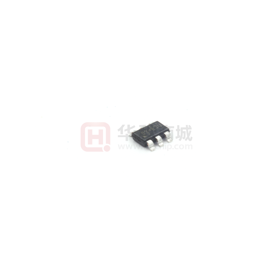
03= : Product Code
03=DNN
3
DNN : Date Code
BOOT GND FB
TSOT-23-6 (FC)
Simplified Application Circuit
VIN
VIN
RT7295A
BOOT
SW
Enable
VOUT
FB
EN
GND
Copyright © 2015 Richtek Technology Corporation. All rights reserved.
DS7295A-07 October 2015
is a registered trademark of Richtek Technology Corporation.
www.richtek.com
1
�RT7295A
Functional Pin Description
Pin No.
Pin Name
Pin Function
1
BOOT
Bootstrap Supply for High-Side Gate Driver. Connect a 0.1F ceramic capacitor
between the BOOT and SW pins.
2
GND
Power Ground.
3
FB
Feedback Voltage Input. The pin is used to set the output voltage of the converter
via a resistive divider. The converter regulates VFB to 0.6V
4
EN
Enable Control Input. Connect EN to a logic-high voltage to enable the IC or to a
logic-low voltage to disable. Do not leave this high impedance input unconnected.
5
VIN
Power Input. The input voltage range is from 4.3V to 18V. Must bypass with a
suitable large ceramic capacitor at this pin.
6
SW
Switch Node. Connect to external L-C filter.
Function Block Diagram
BOOT
VIN
VIN
Reg
PVCC
VIBIAS
VREF
Min off
PVCC
UGATE
OC
Control
SW
Driver
LGATE
UV & OV
GND
PVCC
SW
Ripple
Gen.
+
Comparator
FB
GND SW
VIN
EN
On-Time
SW
EN
Operation
The RT7295A is a synchronous step-down converter with
advanced constant on-time control mode. Using the ACOT
control mode can reduce the output capacitance and fast
transient response. It can minimize the component size
without additional external compensation network.
UVLO Protection
Current Protection
Thermal Shutdown
The inductor current is monitored via the internal switches
cycle-by-cycle. Once the output voltage drops under UV
threshold, the RT7295A will enter hiccup mode.
When the junction temperature exceeds the OTP
threshold value, the IC will shut down the switching
operation. Once the junction temperature cools down and
is lower than the OTP lower threshold, the converter will
autocratically resume switching.
Copyright © 2015 Richtek Technology Corporation. All rights reserved.
www.richtek.com
2
To protect the chip from operating at insufficient supply
voltage, the UVLO is needed. When the input voltage of
VIN is lower than the UVLO falling threshold voltage, the
device will be lockout.
is a registered trademark of Richtek Technology Corporation.
DS7295A-07 October 2015
�RT7295A
Absolute Maximum Ratings
(Note 1)
VIN to GND ----------------------------------------------------------------------------------------------------SW to GND ---------------------------------------------------------------------------------------------------< 10ns ---------------------------------------------------------------------------------------------------------BOOT to GND ------------------------------------------------------------------------------------------------Other Pins -----------------------------------------------------------------------------------------------------Power Dissipation, PD @ TA = 25°C
TSOT-23-6 (FC) ----------------------------------------------------------------------------------------------- 1.429W
Package Thermal Resistance (Note 2)
TSOT-23-6 (FC), θJA ------------------------------------------------------------------------------------------ 70°C/W
TSOT-23-6 (FC), θJC ----------------------------------------------------------------------------------------- 15°C/W
Lead Temperature (Soldering, 10 sec.) ------------------------------------------------------------------ 260°C
Junction Temperature ---------------------------------------------------------------------------------------- 150°C
Storage Temperature Range ------------------------------------------------------------------------------- −65°C to 150°C
ESD Susceptibility (Note 3)
HBM (Human Body Model) --------------------------------------------------------------------------------- 2kV
Recommended Operating Conditions
−0.3V to 20V
−0.3V to (VIN + 0.3V)
−5V to 25V
(VSW − 0.3V) to (VSW + 6V)
−0.3V to 6V
(Note 4)
Supply Input Voltage, VIN ---------------------------------------------------------------------------------- 4.3V to 18V
Junction Temperature Range ------------------------------------------------------------------------------- −40°C to 125°C
Ambient Temperature Range ------------------------------------------------------------------------------- −40°C to 85°C
Electrical Characteristics
(VIN = 12V, TA = 25°C, unless otherwise specified)
Parameter
Symbol
Test Conditions
Min
Typ
Max
Unit
Shutdown Current
ISHDN
VEN = 0V
--
--
4
A
Quiescent Current
IQ
VEN = 2V, VFB = 1V
--
0.5
--
mA
High-Side
RDS(ON)_H
VBOOTSW = 4.8V
--
90
105
Low-Side
RDS(ON)_L
VIN = 5V
--
45
65
Current Limit
ILIM
Valley Current
3.7
4.4
5
A
Oscillator Frequency
f SW
--
500
--
kHz
Maximum Duty Cycle
DMAX
--
90
--
%
Minimum On-Time
tON
--
60
--
ns
Feedback Threshold Voltage
VFB
591
600
609
mV
Logic-High VEN_H
1.19
1.29
1.39
Logic-Low
0.93
1.03
1.13
3.55
3.9
4.25
V
--
340
--
mV
--
800
--
s
Switch-On Resistance
EN Input Threshold
VIN Under-Voltage Lockout
Threshold
VEN_L
VUVLO
VIN Under-Voltage Lockout
Threshold Hysteresis
Soft-Start Time
tSS
Copyright © 2015 Richtek Technology Corporation. All rights reserved.
DS7295A-07 October 2015
In CCM Mode
VIN Rising
m
V
is a registered trademark of Richtek Technology Corporation.
www.richtek.com
3
�RT7295A
Parameter
Symbol
Test Conditions
Min
Typ
Max
Unit
Thermal Shutdown Threshold
TSD
--
160
--
C
Thermal Shutdown Hysteresis
TSD
--
20
--
C
VOUT Discharge Resistance
RDISCHG
EN = 0V, VOUT = 0.5V
--
50
100
UVP Detect
70
75
80
Hysteresis
--
10
--
--
250
--
Output Under-Voltage Trip
Threshold
Output Under-Voltage Delay
Time
%
s
Note 1. Stresses beyond those listed “Absolute Maximum Ratings” may cause permanent damage to the device. These are
stress ratings only, and functional operation of the device at these or any other conditions beyond those indicated in
the operational sections of the specifications is not implied. Exposure to absolute maximum rating conditions may
affect device reliability.
Note 2. θJA is measured at TA = 25°C on a high effective thermal conductivity four-layer test board per JEDEC 51-7. The first
layer of copper area is filled. θJC is measured at the top of the package.
Note 3. Devices are ESD sensitive. Handling precaution is recommended.
Note 4. The device is not guaranteed to function outside its operating conditions.
Copyright © 2015 Richtek Technology Corporation. All rights reserved.
www.richtek.com
4
is a registered trademark of Richtek Technology Corporation.
DS7295A-07 October 2015
�RT7295A
Typical Application Circuit
RT7295A
VIN
4.3V to 18V
5
CIN
10µF
BOOT
VIN
1
SW 6
4 EN
Enable
CBOOT
100nF
L
2µH
CFF
FB 3
R1
10k
R2
10k
GND 2
VOUT
1.2V
COUT
22µF x 2
Table 1. Suggested Component Values
VOUT (V)
R1 (k)
R2 (k)
L (H)
COUT (F)
CFF (pF)
5
110
15
4.7
22 x 2
39
3.3
115
25.5
3.6
22 x 2
33
2.5
25.5
8.06
3.6
22 x 2
NC
1.2
10
10
2
22 x 2
NC
Copyright © 2015 Richtek Technology Corporation. All rights reserved.
DS7295A-07 October 2015
is a registered trademark of Richtek Technology Corporation.
www.richtek.com
5
�RT7295A
Typical Operating Characteristics
Efficiency vs. Load Current
100
90
90
80
80
70
VIN =
VIN =
VIN =
VIN =
60
50
40
Efficiency (%)
Efficiency (%)
Efficiency vs. Load Current
100
4.5V
9V
12V
18V
30
20
VIN = 12V
VIN = 15V
VIN = 18V
70
60
50
40
30
20
10
10
VOUT = 1.2V
0
0.001
0.01
0.1
1
VOUT = 5V
0
0.001
10
0.01
Load Current (A)
0.1
1
10
Load Current (A)
Reference Voltage vs. Temperature
Reference Voltage vs. Input Voltage
0.620
0.65
0.63
Reference Voltage (V)
Reference Voltage (V)
0.615
0.610
0.605
0.600
0.595
0.590
0.585
0.61
0.59
0.57
VIN = 4.5V to 18V, VOUT = 1.2V, IOUT = 0.75A
VIN = 12V, VOUT = 1.2V, IOUT = 0.75A
0.55
0.580
4
5
6
7
8
-50
9 10 11 12 13 14 15 16 17 18
-25
0
Output Voltage vs. Load Current
1.242
540
Switcing Frequency (kHz) a
550
Output Voltage (V)
1.234
VIN = 18V
VIN = 12V
VIN = 9V
1.218
1.210
1.202
1.194
1.186
1.178
VOUT = 1.2V
1.170
0
0.5
1
1.5
2
2.5
3
Load Current (A)
Copyright © 2015 Richtek Technology Corporation. All rights reserved.
www.richtek.com
6
50
75
100
125
Switching Frequency vs. Input Voltage
1.250
1.226
25
Temperature (°C)
Input Voltage (V)
3.5
530
520
510
500
490
480
470
460
VIN = 4.5V to 18V, VOUT = 1.2V, IOUT = 0.75A
450
4
6
8
10
12
14
16
18
Input Voltage (V)
is a registered trademark of Richtek Technology Corporation.
DS7295A-07 October 2015
�RT7295A
Current Limit vs.Temperature
5.0
630
4.9
610
4.8
590
Current Limit (A)
Switching Frequency (kHz) a
Switching Frequency vs. Temperature
650
VIN = 4.5V
VIN = 12V
VIN = 18V
570
550
530
510
4.7
4.6
4.5
4.4
4.3
4.2
490
470
VOUT = 1.2V, IOUT = 0.75A
450
-50
-25
0
25
50
75
100
125
4.1
4.0
-50
-25
0
25
50
75
100
Temperature (°C)
Temperature (°C)
Load Transient Response
Load Transient Response
VOUT
(50mV/Div)
125
VOUT
(50mV/Div)
IOUT
(2A/Div)
VIN = 12V, VOUT = 1.2V, IOUT = 0A to 3.5A
IOUT
(2A/Div)
VIN = 12V, VOUT = 1.2V, IOUT = 1.75A to 3.5A
Time (250μs/Div)
Time (250μs/Div)
Switching
Switching
VOUT
(10mV/Div)
VOUT
(10mV/Div)
VSW
(10V/Div)
VSW
(10V/Div)
I SW
(2A/Div)
I SW
(2A/Div)
VIN = 12V, VOUT = 1.2V, IOUT = 1.75A
Time (1μs/Div)
Copyright © 2015 Richtek Technology Corporation. All rights reserved.
DS7295A-07 October 2015
VIN = 12V, VOUT = 1.2V, IOUT = 3.5A
Time (1μs/Div)
is a registered trademark of Richtek Technology Corporation.
www.richtek.com
7
�RT7295A
Power Off from EN
Power On from EN
VEN
(2V/Div)
VEN
(2V/Div)
VOUT
(1V/Div)
VSW
(10V/Div)
VOUT
(1V/Div)
VSW
(10V/Div)
IOUT
(2A/Div)
IOUT
(2A/Div)
VIN = 12V, VOUT = 1.2V, IOUT = 3.5A
Time (2.5ms/Div)
Time (2.5ms/Div)
Power On from VIN
Power Off from VIN
VIN
(10V/Div)
VOUT
(1V/Div)
VIN
(10V/Div)
VOUT
(1V/Div)
VSW
(10V/Div)
VSW
(10V/Div)
IOUT
(2A/Div)
IOUT
(2A/Div)
VIN = 12V, VOUT = 1.2V, IOUT = 3.5A
Time (2.5ms/Div)
Copyright © 2015 Richtek Technology Corporation. All rights reserved.
www.richtek.com
8
VIN = 12V, VOUT = 1.2V, IOUT = 3.5A
VIN = 12V, VOUT = 1.2V, IOUT = 3.5A
Time (5ms/Div)
is a registered trademark of Richtek Technology Corporation.
DS7295A-07 October 2015
�RT7295A
Application information
Inductor Selection
Selecting an inductor involves specifying its inductance
and also its required peak current. The exact inductor value
is generally flexible and is ultimately chosen to obtain the
best mix of cost, physical size, and circuit efficiency.
Lower inductor values benefit from reduced size and cost
and they can improve the circuit's transient response, but
they increase the inductor ripple current and output voltage
ripple and reduce the efficiency due to the resulting higher
peak currents. Conversely, higher inductor values increase
efficiency, but the inductor will either be physically larger
or have higher resistance since more turns of wire are
required and transient response will be slower since more
time is required to change current (up or down) in the
inductor. A good compromise between size, efficiency,
and transient response is to use a ripple current (ΔIL) about
20% to 40% of the desired full output load current.
Calculate the approximate inductor value by selecting the
input and output voltages, the switching frequency (fSW),
the maximum output current (IOUT(MAX)) and estimating a
ΔIL as some percentage of that current.
VOUT VIN VOUT
L=
VIN fSW IL
Once an inductor value is chosen, the ripple current (ΔIL)
is calculated to determine the required peak inductor
current.
VOUT VIN VOUT
VIN fSW L
I
IL(PEAK) = IOUT(MAX) L
2
IL
IL(VALLY) = IOUT(MAX)
2
Considering the Typical Operating Circuit for 1.2V output
at 3.5A and an input voltage of 12V, using an inductor
ripple of 1.05A (30%), the calculated inductance value is :
IL =
1.2 12 1.2
L=
= 2μH
12 500kHz 1.05
Copyright © 2015 Richtek Technology Corporation. All rights reserved.
DS7295A-07 October 2015
The ripple current was selected at 1.05A and, as long as
we use the calculated 2μH inductance, that should be the
actual ripple current amount. The ripple current and required
peak current as below :
1.2 12 1.2
= 1.05A
12 500kHz 2μH
and IL(PEAK) = 3.5A 1.05 = 4A
2
Inductor saturation current should be chosen over IC's
IL =
current limit.
Input Capacitor Selection
The input filter capacitors are needed to smooth out the
switched current drawn from the input power source and
to reduce voltage ripple on the input. The actual
capacitance value is less important than the RMS current
rating (and voltage rating, of course). The RMS input ripple
current (IRMS) is a function of the input voltage, output
voltage, and load current :
V
VIN
IRMS = IOUT(MAX) OUT
1
VIN
VOUT
Ceramic capacitors are most often used because of their
low cost, small size, high RMS current ratings, and robust
surge current capabilities. However, take care when these
capacitors are used at the input of circuits supplied by a
wall adapter or other supply connected through long, thin
wires. Current surges through the inductive wires can
induce ringing at the RT7295A input which could
potentially cause large, damaging voltage spikes at VIN.
If this phenomenon is observed, some bulk input
capacitance may be required. Ceramic capacitors (to meet
the RMS current requirement) can be placed in parallel
with other types such as tantalum, electrolytic, or polymer
(to reduce ringing and overshoot).
Choose capacitors rated at higher temperatures than
required. Several ceramic capacitors may be paralleled to
meet the RMS current, size, and height requirements of
the application. The typical operating circuit use 10μF and
one 0.1μF low ESR ceramic capacitors on the input.
is a registered trademark of Richtek Technology Corporation.
www.richtek.com
9
�RT7295A
Output Capacitor Selection
The RT7295A is optimized for ceramic output capacitors
and best performance will be obtained using them. The
total output capacitance value is usually determined by
the desired output voltage ripple level and transient response
requirements for sag (undershoot on positive load steps)
and soar (overshoot on negative load steps).
Output Ripple
Output ripple at the switching frequency is caused by the
inductor current ripple and its effect on the output
capacitor's ESR and stored charge. These two ripple
components are called ESR ripple and capacitive ripple.
Since ceramic capacitors have extremely low ESR and
relatively little capacitance, both components are similar
in amplitude and both should be considered if ripple is
critical.
VRIPPLE = VRIPPLE(ESR) VRIPPLE(C)
VRIPPLE(ESR) = IL RESR
VRIPPLE(C) =
IL
8 COUT fSW
For the Typical Operating Circuit for 1.2V output and an
inductor ripple of 1.05A, with 2 x 22μF output capacitance
each with about 5mΩ ESR including PCB trace resistance,
the output voltage ripple components are :
VRIPPLE(ESR) = 1.05A 2.5m = 2.625mV
VRIPPLE(C) =
1.05A
= 5.966mV
8 44μF 500kHz
VRIPPLE = 2.625mV 5.966mV = 8.591mV
Output Transient Undershoot and Overshoot
In addition to voltage ripple at the switching frequency,
the output capacitor and its ESR also affect the voltage
sag (undershoot) and soar (overshoot) when the load steps
up and down abruptly. The ACOT transient response is
very quick and output transients are usually small.
However, the combination of small ceramic output
capacitors (with little capacitance), low output voltages
(with little stored charge in the output capacitors), and
low duty cycle applications (which require high inductance
to get reasonable ripple currents with high input voltages)
increases the size of voltage variations in response to
very quick load changes. Typically, load changes occur
slowly with respect to the IC's 500kHz switching frequency.
Copyright © 2015 Richtek Technology Corporation. All rights reserved.
www.richtek.com
10
But some modern digital loads can exhibit nearly
instantaneous load changes and the following section
shows how to calculate the worst-case voltage swings in
response to very fast load steps.
The output voltage transient undershoot and overshoot each
have two components : the voltage steps caused by the
output capacitor's ESR, and the voltage sag and soar due
to the finite output capacitance and the inductor current
slew rate. Use the following formulas to check if the ESR
is low enough (typically not a problem with ceramic
capacitors) and the output capacitance is large enough to
prevent excessive sag and soar on very fast load step
edges, with the chosen inductor value.
The amplitude of the ESR step up or down is a function of
the load step and the ESR of the output capacitor :
VESR _STEP = ΔIOUT x RESR
The amplitude of the capacitive sag is a function of the
load step, the output capacitor value, the inductor value,
the input-to-output voltage differential, and the maximum
duty cycle. The maximum duty cycle during a fast transient
is a function of the on-time and the minimum off-time since
the ACOTTM control scheme will ramp the current using
on-times spaced apart with minimum off-times, which is
as fast as allowed. Calculate the approximate on-time
(neglecting parasitics) and maximum duty cycle for a given
input and output voltage as :
VOUT
tON
tON =
and DMAX =
VIN fSW
tON tOFF(MIN)
The actual on-time will be slightly longer as the IC
compensates for voltage drops in the circuit, but we can
neglect both of these since the on-time increase
compensates for the voltage losses. Calculate the output
voltage sag as :
VSAG =
L (IOUT )2
2 COUT VIN(MIN) DMAX VOUT
The amplitude of the capacitive soar is a function of the
load step, the output capacitor value, the inductor value
and the output voltage :
VSOAR =
L (IOUT )2
2 COUT VOUT
is a registered trademark of Richtek Technology Corporation.
DS7295A-07 October 2015
�RT7295A
Feed-forward Capacitor (Cff)
Enable Operation (EN)
The RT7295A is optimized for ceramic output capacitors
and for low duty cycle applications. However for high-output
voltages, with high feedback attenuation, the circuit's
response becomes over-damped and transient response
can be slowed. In high-output voltage circuits (VOUT > 3.3V)
transient response is improved by adding a small “feedforward” capacitor (Cff) across the upper FB divider resistor
(figure 1), to increase the circuit's Q and reduce damping
to speed up the transient response without affecting the
steady-state stability of the circuit. Choose a suitable
capacitor value that following below step.
For automatic start-up the EN pin can be connected to
VIN through a 100kΩ resistor. Its large hysteresis band
makes EN useful for simple delay and timing circuits. EN
can be externally pulled to VIN by adding a resistorcapacitor delay (REN and CEN in Figure 2). Calculate the
delay time using EN's internal threshold where switching
operation begins (1.4V, typical).
Get the BW the quickest method to do transient
response form no load to full load. Confirm the damping
frequency. The damping frequency is BW.
An external MOSFET can be added to implement digital
control of EN when no system voltage above 2V is available
(Figure 3). In this case, a 100kΩ pull-up resistor, REN, is
connected between VIN and the EN pin. MOSFET Q1 will
be under logic control to pull down the EN pin. To prevent
enabling circuit when VIN is smaller than the VOUT target
value or some other desired voltage level, a resistive voltage
divider can be placed between the input voltage and ground
and connected to EN to create an additional input under
voltage lockout threshold (Figure 4).
EN
BW
REN
VIN
EN
RT7295A
CEN
GND
VOUT
R1
Figure 2. External Timing Control
Cff
FB
RT7295A
R2
GND
VIN
REN
100k
Q1
Enable
Cff can be calculated base on below equation.
1
Cff
2 3.1412 R1 BW 0.8
Internal Soft-Start (SS)
The RT7295A soft-start uses an internal soft-start time
800μs.
Following below equation to get the minimum capacitance
range in order to avoid UV occur.
RT7295A
GND
Figure 1. Cff Capacitor Setting
EN
Figure 3. Digital Enable Control Circuit
VIN
REN1
REN2
EN
RT7295A
GND
Figure 4. Resistor Divider for Lockout Threshold Setting
COUT VOUT 0.6 1.2
(ILIM Load Current) 0.8
T 800μs
T
Copyright © 2015 Richtek Technology Corporation. All rights reserved.
DS7295A-07 October 2015
is a registered trademark of Richtek Technology Corporation.
www.richtek.com
11
�RT7295A
Output Voltage Setting
Set the desired output voltage using a resistive divider
from the output to ground with the midpoint connected to
FB. The output voltage is set according to the following
equation :
VOUT = 0.6 x (1 + R1 / R2)
VOUT
resistance between BOOT and the external bootstrap
capacitor. This will slow the high-side switch turn-on and
VSW's rise. To remove the resistor from the capacitor
charging path (avoiding poor enhancement due to
undercharging the BOOT capacitor), use the external diode
shown in figure 6 to charge the BOOT capacitor and place
the resistance between BOOT and the capacitor/diode
connection.
5V
R1
FB
RT7295A
R2
BOOT
GND
RT7295A
0.1µF
SW
Figure 5. Output Voltage Setting
Place the FB resistors within 5mm of the FB pin. Choose
R2 between 10kΩ and 100kΩ to minimize power
consumption without excessive noise pick-up and
calculate R1 as follows :
R1
R2 (VOUT 0.6)
0.6
For output voltage accuracy, use divider resistors with 1%
or better tolerance.
External BOOT Bootstrap Diode
When the input voltage is lower than 5.5V it is
recommended to add an external bootstrap diode between
VIN (or VINR) and the BOOT pin to improve enhancement
of the internal MOSFET switch and improve efficiency.
The bootstrap diode can be a low cost one such as 1N4148
or BAT54.
External BOOT Capacitor Series Resistance
The internal power MOSFET switch gate driver is
optimized to turn the switch on fast enough for low power
loss and good efficiency, but also slow enough to reduce
EMI. Switch turn-on is when most EMI occurs since VSW
rises rapidly. During switch turn-off, SW is discharged
relatively slowly by the inductor current during the
deadtime between high-side and low-side switch on-times.
In some cases it is desirable to reduce EMI further, at the
expense of some additional power dissipation. The switch
turn-on can be slowed by placing a small (