®
RT8057
2.25MHz 1A Synchronous Step-Down Converter
General Description
Features
The RT8057 is a high efficiency Pulse-Width-Modulated
(PWM) step-down DC/DC converter, capable of delivering
1A output current over a wide input voltage range from 2.7V
to 5.5V. The RT8057 is ideally suited for portable electronic
devices that are powered from 1-cell Li-ion battery or from
other power sources such as cellular phones, PDAs, handheld devices, game console and related accessories.
2.7V to 5.5V Wide Input Operation Range
2.25MHz Fixed-Frequency PWM Operation
Up to 1A Output Current
Up to 90% Efficiency
0.6V Reference Allows Low Output Voltage
Internal Soft-Start
No Schottky Diode Required
Internal Compensation to Reduce External
Components
Low Dropout Operation : 100% Duty Cycle
RoHS Compliant and Halogen Free
The internal synchronous rectifier with low R DS(ON)
dramatically reduces conduction loss at PWM mode.
No external Schottky diode is required in practical
applications. The RT8057 enters Low Dropout Mode when
normal Pulse -Width Mode cannot provide regulated output
voltage by continuously turning on the upper P-MOSFET.
The RT8057 enters shut-down mode and consumes less
than 1μA when the EN pin is pulled low. The switching
ripple is easily smoothed-out by small package filtering
elements due to a fixed operating frequency of 2.25MHz.
Applications
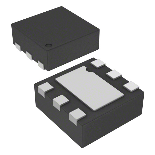
The RT8057 is available in a small WDFN-6SL 2x2 package.
Ordering Information
RT8057
Portable Instruments
Game Console and Accessories
Microprocessors and DSP Core Supplies
Cellular Phones
Wireless and DSL Modems
PC Cards
Pin Configurations
(2)
(TOP VIEW)
Package Type
QW : WDFN-6SL 2x2 (W-Type)
Lead Plating System
G : Green (Halogen Free and Pb Free)
Note :
Richtek products are :
1
2
3
7
6
GND
5
VIN
EN
4
WDFN-6SL 2x2
Marking Information
J7 : Product Code
RoHS compliant and compatible with the current requirements of IPC/JEDEC J-STD-020.
LX
NC
FB
GND
Taping Type ( Pin1 at Q2)
J7W
W : Date Code
Suitable for use in SnPb or Pb-free soldering processes.
Copyright © 2014 Richtek Technology Corporation. All rights reserved.
DS8057-04 February 2014
is a registered trademark of Richtek Technology Corporation.
www.richtek.com
1
�RT8057
Typical Application Circuit
RT8057
5
VIN
CIN
4.7µF
LX
VIN
1
L1
2.2µH
VOUT
2.3V
4 EN
6, 7 (Exposed Pad)
C1
10pF
FB
3
R1
680k
COUT
10µF
R2
240k
GND
Function Pin Description
Pin No.
Pin Name
Pin Function
1
LX
Switch Node. Connect to the external inductor.
2
NC
No Internal Connection. Connect to GND.
3
FB
Feedback Pin. Connect to the external resistor divider.
4
EN
Chip Enable (Active High).
5
VIN
Power Input. Connect to the input capacitor.
6,
GND
7 (Exposed Pad)
Power GND. The Exposed Pad must be soldered to a large PCB and connected
to GND for maximum power dissipation.
Function Block Diagram
EN
OSC &
Shutdown
Control
Slope
Compensation
VIN
RS1
Current
Limit
Detector
Current
Sense
FB
Error
Amplifier
RC
Control
Logic
Driver
LX
PWM
Comparator
RS2
COMP
UVLO &
Power Good
Detector
Copyright © 2014 Richtek Technology Corporation. All rights reserved.
www.richtek.com
2
GND
VREF
is a registered trademark of Richtek Technology Corporation.
DS8057-04 February 2014
�RT8057
Absolute Maximum Ratings
(Note 1)
Supply Input Voltage, VIN -----------------------------------------------------------------------------------------------Power Dissipation, PD @ TA = 25°C
WDFN-6SL 2x2 -----------------------------------------------------------------------------------------------------------Package Thermal Resistance (Note 2)
WDFN-6SL 2x2, θJA ------------------------------------------------------------------------------------------------------WDFN-6SL 2x2, θJC -----------------------------------------------------------------------------------------------------Lead Temperature (Soldering, 10 sec.) ------------------------------------------------------------------------------Junction Temperature ----------------------------------------------------------------------------------------------------Storage Temperature Range -------------------------------------------------------------------------------------------ESD Susceptibility (Note 3)
HBM -------------------------------------------------------------------------------------------------------------------------MM ----------------------------------------------------------------------------------------------------------------------------
Recommended Operating Conditions
6.5V
0.606W
165°C/W
8.2°C/W
260°C
150°C
−65°C to 150°C
2kV
200V
(Note 4)
Supply Input Voltage, VIN ------------------------------------------------------------------------------------------------ 2.7V to 5.5V
Junction Temperature Range -------------------------------------------------------------------------------------------- −40°C to 125°C
Ambient Temperature Range -------------------------------------------------------------------------------------------- −40°C to 85°C
Electrical Characteristics
(VIN = 3.6V, TA = 25°C unless otherwise specified)
Parameter
Symbol
Test Conditions
Min
Typ
Max
Unit
Output Current
IOUT
VIN = 2.7V to 5.5V
--
--
1
A
Quiescent Current
IQ
IOUT = 0mA
--
81
--
A
Reference Voltage (0.6V)
VREF
2
--
2
2.5
--
2.5
VIN Rising
2
2.2
2.4
V
Hysteresis
--
0.2
--
V
--
0.1
1
A
--
2.25
--
MHz
Under Voltage Lockout Threshold VUVLO
Shutdown Current
Note 5
ISHDN
Switching Frequency
%
EN Threshold Logic-High
Voltage
Logic-Low
VIH
1
--
VIN
V
VIL
--
--
0.4
V
Thermal Shutdown Temperature
TSD
--
150
--
°C
High Side
RDS(ON)_H ISW = 0.2A
--
250
--
m
Low Side
RDS(ON)_L ISW = 0.2A
--
200
--
m
1.1
1.5
2
A
Switch On
Resistance
Peak Current Limit
ILIM
Output Voltage Line Regulation
VIN = 2.7V to 5.5V
--
--
1
%/V
Output Voltage Load Regulation
0mA < IOUT < 0.6A
--
--
1
%
200
300
400
s
Start-Up Time
tss
Guaranteed by Design
Copyright © 2014 Richtek Technology Corporation. All rights reserved.
DS8057-04 February 2014
is a registered trademark of Richtek Technology Corporation.
www.richtek.com
3
�RT8057
Note 1. Stresses beyond those listed “Absolute Maximum Ratings” may cause permanent damage to the device. These are stress
ratings only, and functional operation of the device at these or any other conditions beyond those indicated in the operational
sections of the specifications is not implied. Exposure to absolute maximum rating conditions may affect device reliability.
Note 2. θJA is measured in natural convection at TA = 25°C on a low-effective thermal conductivity test board of JEDEC 51-3 thermal
measurement standard. The measurement case position of θJC is on the exposed pad of the package.
Note 3. Devices are ESD sensitive. Handling precaution is recommended.
Note 4. The device is not guaranteed to function outside its operating conditions.
Note 5. The reference voltage accuracy is ±2.5% at recommended ambient temperature range, guaranteed by design.
Copyright © 2014 Richtek Technology Corporation. All rights reserved.
www.richtek.com
4
is a registered trademark of Richtek Technology Corporation.
DS8057-04 February 2014
�RT8057
Typical Operating Characteristics
Output Voltage vs. Input Voltage
Efficiency vs. Output Current
2.38
100
VIN = 5V
90
2.36
VIN = 3.3V
Output Voltage (V)
Efficiency (%)
80
70
60
50
40
30
2.34
2.32
2.30
2.28
2.26
20
2.24
10
VOUT = 2.3V, IOUT = 0A
VOUT = 2.3V
0
2.22
0.0
0.2
0.4
0.6
0.8
1.0
2.5
3.0
3.5
4.0
4.5
5.0
5.5
Input Voltage (V)
Output Current (A)
Frequency vs. Input Voltage
Frequency vs. Temperature
2.40
2.30
2.35
2.25
2.30
2.20
Frequency (MHz)1
Frequency (MHz)1
VIN = 3.3V
2.25
2.20
2.15
2.10
2.05
VIN = 5V
2.15
2.10
2.05
2.00
1.95
VIN = 5V, VOUT = 2.3V,
IOUT = 0.2A
VOUT = 2.3V, IOUT = 0.2A
1.90
2.00
2.5
3.0
3.5
4.0
4.5
5.0
-50
5.5
-25
0
Output Current Limit vs. Input Voltage
50
75
100
125
Output Current Limit vs. Temperature
1.6
1.6
1.5
1.5
Output Current Limit (A)
Output Current limit (A)
25
Temperature (°C)
Input Voltage (V)
1.4
1.3
1.2
1.1
1.4
1.3
1.2
1.1
VOUT = 2.3V
VIN = 5V, VOUT = 2.3V
1.0
1.0
2.5
3.0
3.5
4.0
4.5
5.0
Input Voltage (V)
Copyright © 2014 Richtek Technology Corporation. All rights reserved.
DS8057-04 February 2014
5.5
-50
-25
0
25
50
75
100
125
Temperature (°C)
is a registered trademark of Richtek Technology Corporation.
www.richtek.com
5
�RT8057
Reference Voltage vs. Temperature
Output Voltage vs. Temperature
0.608
2.34
0.606
Reference Voltage (V)
2.35
Output Voltage (V)
2.33
2.32
2.31
2.30
2.29
2.28
2.27
VIN = 5V, VOUT = 2.3V,
IOUT = 0A
2.26
0.604
0.602
0.600
0.598
0.596
0.594
VIN = 5V, VOUT = 2.3V
0.592
2.25
-50
-25
0
25
50
75
100
125
-50
25
50
75
100
125
Output Ripple
Output Ripple
VLX
(5V/Div)
VOUT
(5mV/Div)
VOUT
(5mV/Div)
VIN = 3.3V, VOUT = 2.3V,
IOUT = 1A
VIN = 5V, VOUT = 2.3V, IOUT = 1A
Time (250ns/Div)
Time (250ns/Div)
Load Transient Response
Load Transient Response
VOUT
(100mV/Div)
VOUT
(100mV/Div)
IOUT
(500mA/Div)
IOUT
(500mA/Div)
VIN = 5V, VOUT = 2.3V,
IOUT = 0A to 1A
Time (100μs/Div)
Copyright © 2014 Richtek Technology Corporation. All rights reserved.
www.richtek.com
6
0
Temperature (°C)
Temperature (°C)
VLX
(5V/Div)
-25
VIN = 5V, VOUT = 2.3V,
IOUT = 0.4A to 1A
Time (100μs/Div)
is a registered trademark of Richtek Technology Corporation.
DS8057-04 February 2014
�RT8057
Power On from EN
Power Off from EN
VIN = 5V, VOUT = 2.3V,
IOUT = 1A
VEN
(2V/Div)
VEN
(2V/Div)
VOUT
(2V/Div)
VOUT
(2V/Div)
IOUT
(500mA/Div)
VIN = 5V, VOUT = 2.3V,
IOUT = 1A
IOUT
(500mA/Div)
Time (100μs/Div)
Time (100μs/Div)
UVLO vs. Temperature
En Threshold vs. Temperature
0.80
2.4
2.3
0.78
Turn On
EN Threshold (V)
UVLO (V)
Turn On
0.76
2.2
2.1
Turn Off
2.0
1.9
1.8
1.7
0.74
0.72
0.70
0.68
0.66
Turn Off
0.64
1.6
0.62
VIN = 5V, VOUT = 2.3V
VOUT = 2.3V
0.60
1.5
-50
-25
0
25
50
75
100
125
-50
-25
0
25
50
75
100
125
Temperature (°C)
Temperature (°C)
Output Voltage vs. Output Current
2.34
Output Voltage (V)
2.33
2.32
2.31
2.30
2.29
2.28
2.27
VIN = 5V, VOUT = 2.3V
2.26
0.0
0.1
0.2
0.3
0.4
0.5
0.6
0.7
0.8
0.9
1.0
Output Current (A)
Copyright © 2014 Richtek Technology Corporation. All rights reserved.
DS8057-04 February 2014
is a registered trademark of Richtek Technology Corporation.
www.richtek.com
7
�RT8057
Application Information
The basic RT8057 application circuit is shown in Typical
Application Circuit. External component selection is
determined by the maximum load current and begins with
the selection of the inductor value and operating frequency
followed by CIN and COUT.
Output Voltage Setting
The output voltage is set by an external resistive divider
according to the following equation :
R1
VOUT VREF x (1
)
R2
where VREF equals to 0.6V typical. The resistive divider
allows the FB pin to sense a fraction of the output voltage
as shown in Figure 1.
VOUT
The RT8057 is designed to operate down to an input supply
voltage of 2.7V. One important consideration at low input
supply voltages is that the RDS(ON) of the P-Channel and
N-Channel power switches increases. The user should
calculate the power dissipation when the RT8057 is used
at 100% duty cycle with low input voltages to ensure that
thermal limits are not exceeded.
Under Voltage Protection (UVP)
The output voltage can be continuously monitored for under
voltage protection. When the output voltage is less than
33% of its set voltage threshold after OCP occurs, the
under voltage protection circuit will be triggered to auto
re-soft-start.
Input Voltage Over Voltage protection (VIN OVP)
R1
FB
RT8057
Low Supply Operation
When the input voltage (VIN) is higher than 6V, VIN OVP
will be triggered and the IC stops switching. Once the
input voltage drops below 6V, the IC will return to normal
operation.
R2
GND
Figure 1. Setting the Output Voltage
Output Over Voltage Protection (VOUT OVP)
Soft-Start
The RT8057 contains an internal soft-start clamp that
gradually raises the clamp on the FB pin.
100% Duty Cycle Operation
When the input supply voltage decreases toward the output
voltage, the duty cycle increases toward the maximum
on-time. Further reduction of the supply voltage forces
the main switch to remain on for more than one cycle,
eventually reaching 100% duty cycle.
The output voltage will then be determined by the input
voltage minus the voltage drop across the internal
P-MOSFET and the inductor.
When the output voltage exceeds more than 5% of the
nominal reference voltage, the feedback loop forces the
internal switches off within 50μs. Therefore, the output
over voltage protection is automatically triggered by the
loop.
Short Circuit Protection
When the output is shorted to ground, the inductor current
decays very slowly during a single switching cycle. A
current runaway detector is used to monitor inductor
current. As current increases beyond the control of current
loop, switching cycles will be skipped to prevent current
runaway from occurring.
Table 1. Inductors
Component
Supplier
TAIYO YUDEN
Series
NR4018
T2R2M
Inductance (H)
2.2H
Copyright © 2014 Richtek Technology Corporation. All rights reserved.
www.richtek.com
8
DCR (m)
60
Current Rating (mA)
2700
Dimensions (mm)
4 X 4 X 1.8
is a registered trademark of Richtek Technology Corporation.
DS8057-04 February 2014
�RT8057
CIN and COUT Selection
The input capacitance, C IN, is needed to filter the
trapezoidal current at the source of the top MOSFET. To
prevent large ripple voltage, a low ESR input capacitor
sized for the maximum RMS current should be used. RMS
current is given by :
IRMS IOUT(MAX)
VOUT
VIN
VIN
1
VOUT
This formula has a maximum at VIN = 2VOUT, where IRMS =
IOUT/2. This simple worst case condition is commonly used
for design because even significant deviations do not result
in much difference. Choose a capacitor rated at a higher
temperature than required.
Several capacitors may also be paralleled to meet size or
height requirements in the design.
The selection of COUT is determined by the effective series
resistance (ESR) that is required to minimize voltage ripple
and load step transients, as well as the amount of bulk
capacitance that is necessary to ensure that the control
loop is stable. Loop stability can be checked by viewing
the load transient response. The output ripple, ΔVOUT, is
determined by :
1
VOUT IL ESR
8fCOUT
The output ripple is highest at maximum input voltage
since ΔIL increases with input voltage. Multiple capacitors
placed in parallel may be needed to meet the ESR and
RMS current handling requirements. Dry tantalum, special
polymer, aluminum electrolytic and ceramic capacitors are
all available in surface mount packages. Special polymer
capacitors offer very low ESR, but have lower capacitance
density than other types. Tantalum capacitors have the
highest capacitance density, but it is important to only
use types that have been surge tested for use in switching
power supplies. Aluminum electrolytic capacitors have
significantly higher ESR, but can be used in cost-sensitive
applications provided that consideration is given to ripple
current ratings and long term reliability. Ceramic capacitors
have excellent low ESR characteristics, but can have a
high voltage coefficient and audible piezoelectric effects.
The high Q of ceramic capacitors with trace inductance
can also lead to significant ringing.
Using Ceramic Input and Output Capacitors
Higher value, lower cost ceramic capacitors are now
becoming available in smaller case sizes. Their high ripple
current, high voltage rating and low ESR make them ideal
for switching regulator applications. However, care must
be taken when these capacitors are used at the input and
output. When a ceramic capacitor is used at the input
and the power is supplied by a wall adapter through long
wires, a load step at the output can induce ringing at the
input, VIN. At best, this ringing can couple to the output
and be mistaken as loop instability. At worst, a sudden
inrush of current through the long wires can potentially
cause a voltage spike at VIN large enough to damage the
part.
Table 2. Capacitors for CIN and COUT
Component Supplier
Part No.
Capacitance (F)
Case Size
MuRata
GRM31CR71A475KA01
4.7F
1206
MuRata
GRM31CR71A106KA01
10F
1206
Copyright © 2014 Richtek Technology Corporation. All rights reserved.
DS8057-04 February 2014
is a registered trademark of Richtek Technology Corporation.
www.richtek.com
9
�RT8057
Thermal Considerations
Layout Considerations
For continuous operation, do not exceed absolute
maximum junction temperature. The maximum power
dissipation depends on the thermal resistance of the IC
package, PCB layout, rate of surrounding airflow, and
difference between junction and ambient temperature. The
maximum power dissipation can be calculated by the
following formula :
Follow the PCB layout guidelines for optimal performance
of the RT8057.
LX node experiences high frequency voltage swing and
should be kept within a small area. Keep all sensitive
small-signal nodes away from the LX node to prevent
stray capacitive noise pick up.
PD(MAX) = (TJ(MAX) − TA) / θJA
where TJ(MAX) is the maximum junction temperature, TA is
the ambient temperature, and θJA is the junction to ambient
thermal resistance.
For recommended operating condition specifications of
the RT8057, the maximum junction temperature is 125°C
and TA is the ambient temperature. The junction to ambient
thermal resistance, θ JA , is layout dependent. For
WDFN-6SL 2x2 packages, the thermal resistance, θJA, is
165°C/W on a standard JEDEC 51-3 single-layer thermal
test board. The maximum power dissipation at TA = 25°C
can be calculated by the following formula :
PD(MAX) = (125°C − 25°C) / (165°C/W) = 0.606W for
WDFN-6SL 2x2 package
Connect the terminal of the input capacitor(s), CIN, as
close as possible to the VIN pin. This capacitor provides
the AC current into the internal power MOSFETs.
Flood all unused areas on all layers with copper. Flooding
with copper will reduce the temperature rise of power
components. Connect the copper areas to any DC net
(VIN, VOUT, GND, or any other DC rail in the system).
Connect the FB pin directly to the feedback resistors.
The resistive voltage divider must be connected between
VOUT and GND.
LX should be connected to inductor by
wide and short trace. Keep sensitive
components away from this trace.
COUT
VOUT
VOUT
LX
1
NC
C1 FB
2
GND
L1
The maximum power dissipation depends on the operating
ambient temperature for fixed T J(MAX) and thermal
resistance, θJA. For the RT8057 package, the derating
curve in Figure 2 allows the designer to see the effect of
rising ambient temperature on the maximum power
dissipation.
3
7
R1
R2
6
GND
5
VIN
EN
4
CIN
Input capacitor must
be placed as close to
the IC as possible.
Maximum Power Dissipation (W)1
Figure 3. PCB Layout Guide
0.65
0.60
0.55
0.50
0.45
0.40
0.35
0.30
0.25
0.20
0.15
0.10
0.05
0.00
Single-Layer PCB
0
25
50
75
100
125
Ambient Temperature (°C)
Figure 2. Derating Curve for the RT8057 Package
Copyright © 2014 Richtek Technology Corporation. All rights reserved.
www.richtek.com
10
is a registered trademark of Richtek Technology Corporation.
DS8057-04 February 2014
�RT8057
Outline Dimension
D2
D
L
E
E2
1
e
2
b
A
A1
SEE DETAIL A
1
2
1
DETAIL A
Pin #1 ID and Tie Bar Mark Options
A3
Note : The configuration of the Pin #1 identifier is optional,
but must be located within the zone indicated.
Dimensions In Millimeters
Dimensions In Inches
Symbol
Min
Max
Min
Max
A
0.700
0.800
0.028
0.031
A1
0.000
0.050
0.000
0.002
A3
0.175
0.250
0.007
0.010
b
0.200
0.350
0.008
0.014
D
1.900
2.100
0.075
0.083
D2
1.550
1.650
0.061
0.065
E
1.900
2.100
0.075
0.083
E2
0.950
1.050
0.037
0.041
e
L
0.650
0.200
0.026
0.300
0.008
0.012
W-Type 6SL DFN 2x2 Package
Richtek Technology Corporation
14F, No. 8, Tai Yuen 1st Street, Chupei City
Hsinchu, Taiwan, R.O.C.
Tel: (8863)5526789
Richtek products are sold by description only. Richtek reserves the right to change the circuitry and/or specifications without notice at any time. Customers should
obtain the latest relevant information and data sheets before placing orders and should verify that such information is current and complete. Richtek cannot
assume responsibility for use of any circuitry other than circuitry entirely embodied in a Richtek product. Information furnished by Richtek is believed to be
accurate and reliable. However, no responsibility is assumed by Richtek or its subsidiaries for its use; nor for any infringements of patents or other rights of third
parties which may result from its use. No license is granted by implication or otherwise under any patent or patent rights of Richtek or its subsidiaries.
DS8057-04 February 2014
www.richtek.com
11
�