物料型号:RT8064
器件简介:
RT8064是一款简单易用的电流模式控制的2A同步降压DC-DC转换器,输入电压范围为2.7V至5.5V。该设备内置了精确的0.8V参考电压,并集成了低RDS(ON)功率MOSFET,以实现在WDFN-8L 3x3和SOP-8(暴露垫)封装中的高效率。
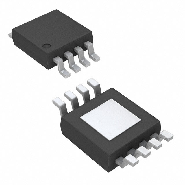
引脚分配:
- SOP-8 (Exposed Pad)和WDFN-8L 3x3两种封装类型。
- 引脚包括COMP(补偿节点)、SS(软启动电容连接节点)、EN(使能控制输入)、VIN(电源输入)、LX(开关节点)、RT(振荡器电阻输入)、FB(反馈电压输入)、PGOOD(电源良好指示)和GND(地)。
参数特性:
- 输入电压范围:2.7V至5.5V。
- 集成180mΩ和120mΩ FETs。
- 100%占空比,最低降额。
- 轻载时的节能模式。
- 可调频率:200kHz至2MHz。
- 0.8V参考电压允许低输出电压。
- 使能功能、外部软启动、电源良好功能、输入欠压锁定保护、输出欠压保护和过温保护。
功能详解:
- RT8064在自动PSM(功率节省模式)下运行,以在轻载操作期间保持高效率。
- 设备具有周期性电流限制保护,以防止在输出短路、过电流或电感饱和时设备遭受灾难性损坏。
- 可调软启动功能可防止启动期间的浪涌电流。
- 设备还具有输入欠压锁定、输出欠压保护和过温保护,以确保在所有操作条件下安全平稳运行。
应用信息:
适用于LCD电视和监视器、笔记本电脑、分布式电源系统、IP电话和数字相机等。
封装信息:
- SOP-8 (Exposed Pad-Option 2)和WDFN-8L 3x3 (W-Type)两种封装选项。
- 引脚镀层系统包括ECO(无卤素和无铅的生态元素)。