®
RT8072
5A, 2MHz, High Efficiency Synchronous Step-Down Converter
General Description
Features
The RT8072 is a high efficiency PWM step-down converter
and capable of delivering 5A output current over a wide
input voltage range from 2.9V to 5.5V.
The RT8072 provides accurate regulation for a variety of
loads with an ±1% reference voltage at room temperature.
For reducing inductor size, it provides up to 2MHz
switching frequency. The efficiency is maximized through
the integrated 50mΩ for high side, 35mΩ for low side
MOSFETs and 250μA typical supply current.
The RT8072 features over current protection, frequency
fold back function in shorted circuit, hiccup mode under
voltage protection and over temperature protection.
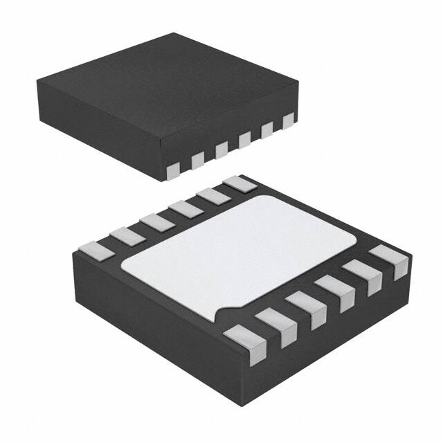
The RT8072 is available in SOP-8 (Exposed Pad) and
WDFN-12L 3x3 packages.
Ω MOSFETs
Integrated 50mΩ
Ω and 35mΩ
5A Output Current
High Efficiency Up to 95%
2.9V to 5.5V Input Range
Adjustable PWM Frequency : 300kHz to 2MHz
0.8V ±1% Reference Voltage
Adjustable External Soft-Start
Power Good Indicator (WDFN-12L 3x3 Only)
Over Current Protection
Under Voltage Protection
Over Temperature Protection
SOP-8 (Exposed Pad) and 12-Lead WDFN Packages
RoHS Compliant and Halogen Free
Applications
Ordering Information
RT8072
Package Type
SP : SOP-8 (Exposed Pad-Option 2)
QW : WDFN-12L 3x3 (W-Type)
(Exposed Pad-Option 1)
Low Voltage, High Density Power Systems
Distributed Power Systems
Point-of-Load Conversions
Marking Information
RT8072GSP
RT8072GSP : Product Number
RT8072
GSPYMDNN
Lead Plating System
G : Green (Halogen Free and Pb Free)
YMDNN : Date Code
Note :
RT8072GQW
Richtek products are :
6C= : Product Code
RoHS compliant and compatible with the current require-
YMDNN : Date Code
6C=YM
DNN
ments of IPC/JEDEC J-STD-020.
Suitable for use in SnPb or Pb-free soldering processes.
Simplified Application Circuit
VIN
VIN
BOOT
RT8072
CIN
CBOOT
L
LX
EN
RC
CC
RT
RT
RFB1
FB
GND
Copyright © 2020 Richtek Technology Corporation. All rights reserved.
DS8072-03 August 2020
VOUT
COUT
COMP
RFB2
is a registered trademark of Richtek Technology Corporation.
www.richtek.com
1
�RT8072
Pin Configuration
COMP
GND
2
EN
3
VIN
4
PGND
8
FB
7
RT
6
LX
5
BOOT
9
COMP
PGOOD
SS
EN
VIN
VIN
SOP-8 (Exposed Pad)
1
2
3
4
5
6
PGND
(TOP VIEW)
13
12
11
10
9
8
7
FB
RT
LX
LX
LX
BOOT
WDFN-12L 3x3
Functional Pin Description
Pin No.
Pin Function
Pin Name
SOP-8
(Exposed Pad)
WDFN-12L 3x3
1
1
COMP
Compensation Node.
2
--
GND
Analog Ground.
3
4
EN
Chip Enable. Externally pulled high to enable and pulled low to
disable this chip, and it is internally pulled up to high when the
pin is floating.
4
5, 6
VIN
Power Input.
5
7
BOOT
Bootstrap Supply for High Side Gate Driver.
6
8, 9, 10
LX
Switch Node.
7
11
RT
Frequency Setting.
8
12
FB
Feedback Voltage Input.
9
13
(Exposed Pad)
PGND
Power Ground. The exposed pad must be shouldered to a
large PCB and connected to PGND for maximum power
dissipation.
--
2
PGOOD
Power Good Indicator with Open Drain Output. It is high
impedance when the output voltage is regulated. It is internally
pulled low when the chip is shutdown, thermal shutdown or
VIN is under UVLO threshold.
--
3
SS
Soft-Start Control.
Copyright © 2020 Richtek Technology Corporation. All rights reserved.
www.richtek.com
2
is a registered trademark of Richtek Technology Corporation.
DS8072-03 August 2020
�RT8072
Functional Block Diagram
For SOP-8 (Exposed Pad) Package
VIN
VIN
Over Temperature
Protection
Internal
pull up
current
EN
EN Threshold
UVLO
Shutdown
Control
Current
Sense
GND
BOOT
RT
Oscillator
Control
Logic
Slope
Compensation
Soft-Start
Driver
LX
PWM
Comparator
Voltage
Reference
Error
Amplifier
FB
PGND
COMP
For WDFN-12L 3x3 Package
VIN
VIN
Internal
pull up
current
EN
EN Threshold
RT
UVLO
Shutdown
Control
Current
Sense
BOOT
Oscillator
VIN
SS
Over Temperature
Protection
SoftStart
Voltage
Reference
Control
Logic
Slope
Compensation
Driver
LX
PWM
Comparator
Error
Amplifier
PGND
FB
PGOOD
Power Good
Threshold
COMP
Copyright © 2020 Richtek Technology Corporation. All rights reserved.
DS8072-03 August 2020
is a registered trademark of Richtek Technology Corporation.
www.richtek.com
3
�RT8072
Operation
The RT8072 is a current mode synchronous step-down
DC/DC converter with two integrated power MOSFETs. It
can deliver up to 5A output current from a 2.9V to 5.5V
input supply. The RT8072's current mode architecture
allows the transient response to be optimized over a wide
input voltage and load range. Cycle-by-cycle current limit
provides protection against shorted outputs and soft-start
eliminates input current surge during start-up.
PGOOD Comparator
When the feedback voltage (VFB) rises above 94% or falls
below 106% of reference voltage, the PGOOD open drain
output will be high impedance. The PGOOD open drain
output will be internally pulled low when the feedback
voltage (VFB) falls below 90% or rises above 110% of
reference voltage.
Soft-Start (SS)
Error Amplifier
The error amplifier adjusts COMP voltage by comparing
the feedback signal (VFB) from the output voltage with the
internal 0.8V reference. When the load current increases,
it causes a drop in the feedback voltage relative to the
reference. The COMP voltage then rises to allow higher
inductor current to match the load current.
Oscillator (OSC)
The internal oscillator provides switching frequency from
300kHz to 2MHz, and is adjusted by an external resistor.
Copyright © 2020 Richtek Technology Corporation. All rights reserved.
www.richtek.com
4
An internal current source charges an external capacitor
to build the soft-start ramp voltage (VSS). The VFB voltage
will track the VSS during soft-start interval. The chip will
use internal soft-start if the SS pin is floating. The nominal
internal soft-start time is 800μs.
Over Temperature Protection (OTP)
The RT8072 implements an internal over temperature
protection. When junction temperature is higher than
165°C, it will stop switching operation. Once the junction
temperature decreases below 145°C, the RT8072 will
automatically resume switching.
is a registered trademark of Richtek Technology Corporation.
DS8072-03 August 2020
�RT8072
Absolute Maximum Ratings
(Note 1)
Supply Input Voltage, VIN ----------------------------------------------------------------------------------------BOOT to LX ----------------------------------------------------------------------------------------------------------Other Pins ------------------------------------------------------------------------------------------------------------Power Dissipation, PD @ TA = 25°C
SOP-8 (Exposed Pad) --------------------------------------------------------------------------------------------WDFN-12L 3x3 ------------------------------------------------------------------------------------------------------Package Thermal Resistance (Note 2)
SOP-8 (Exposed Pad), θJA ---------------------------------------------------------------------------------------SOP-8 (Exposed Pad), θJC --------------------------------------------------------------------------------------WDFN-12L 3x3, θJA ------------------------------------------------------------------------------------------------WDFN-12L 3x3, θJC ------------------------------------------------------------------------------------------------Lead Temperature (Soldering, 10 sec.) ------------------------------------------------------------------------Junction Temperature ----------------------------------------------------------------------------------------------Storage Temperature Range -------------------------------------------------------------------------------------ESD Susceptibility (Note 3)
HBM (Human Body Model) ----------------------------------------------------------------------------------------
Recommended Operating Conditions
−0.3V to 6.5V
−0.3V to 6V
−0.3V to (VIN + 0.3V)
2.041W
1.667W
49°C/W
15°C/W
60°C/W
7.5°C/W
260°C
150°C
−65°C to 150°C
2kV
(Note 4)
Supply Input Voltage, VIN ----------------------------------------------------------------------------------------- 2.9V to 5.5V
Junction Temperature Range -------------------------------------------------------------------------------------- −40°C to 125°C
Ambient Temperature Range -------------------------------------------------------------------------------------- −40°C to 85°C
Electrical Characteristics
(VIN = 5V, CIN = 10μF, TA = 25°C, unless otherwise specified)
Parameter
Symbol
Test Conditions
Min
Typ
Max
Unit
Input Power Supply
Under Voltage Lockout Threshold
VUVLO
VIN Rising
--
2.6
2.8
V
Quiescent Current
IQ
Active, VFB = 0.9V, Not switching
--
250
--
A
Shutdown Current
ISHDN
--
2
5
A
VREF
0.792
0.8
0.808
V
Voltage Reference
Voltage Reference
Enable
Logic-High
VIH
1.5
--
5.5
Logic-Low
VIL
--
--
0.4
300
--
2000
RT = 28.7k
--
1400
--
RT pin is floating
--
300
--
WDFN-12L 3x3 Only
--
±7
--
%
Minimum On-Time
--
80
--
ns
Minimum Off-Time
--
60
--
ns
EN Input Voltage
V
Switching Frequency Setting
Switching Frequency
Power Good Range
fOSC
Copyright © 2020 Richtek Technology Corporation. All rights reserved.
DS8072-03 August 2020
kHz
is a registered trademark of Richtek Technology Corporation.
www.richtek.com
5
�RT8072
Parameter
Symbol
Test Conditions
Min
Typ
Max
Unit
MOSFET
High Side MOSFET On-resistance
VIN = 5V, BOOT LX = 5V
--
50
--
m
Low Side MOSFET On-resistance
VIN = 5V
--
35
--
m
6
8
--
A
VFB Rising (Good)
--
94
--
VFB Falling (Fault)
--
90
--
VFB Rising (Fault)
--
110
--
VFB Falling (Good)
--
106
--
Rising
--
165
--
C
--
20
--
C
Current Limit
Current Limit Threshold
Power Good
Power Good Range
% VREF
Over Temperature Protection
Thermal Shutdown
Thermal Shutdown Hysteresis
Note 1. Stresses beyond those listed “Absolute Maximum Ratings” may cause permanent damage to the device. These are
stress ratings only, and functional operation of the device at these or any other conditions beyond those indicated in
the operational sections of the specifications is not implied. Exposure to absolute maximum rating conditions may
affect device reliability.
Note 2. θJA is measured at TA = 25°C on a high effective thermal conductivity four-layer test board per JEDEC 51-7. θJC is
measured at the exposed pad of the package.
Note 3. Devices are ESD sensitive. Handling precaution is recommended.
Note 4. The device is not guaranteed to function outside its operating conditions.
Copyright © 2020 Richtek Technology Corporation. All rights reserved.
www.richtek.com
6
is a registered trademark of Richtek Technology Corporation.
DS8072-03 August 2020
�RT8072
Typical Application Circuit
VIN
VIN
CIN1
10µF
CIN2
10µF
BOOT
RT8072
RPG
100k
CBOOT
0.22µF
VOUT
L
LX
PGOOD
Chip Enable
EN
COUT1
10µF
PGND
RFB1
SS
CSS
10nF
COMP
CHF*
COUT3
47µF to
100µF
GND
RT
RT
28.7k
COUT2
10µF
FB
RC
RFB2
CC
* : Option
Table 1. Recommended Component Selection
RFB2
CC (nF)
L (H)
RC (k)
(k)
1.2
33
0.33
0.47
3.3
RFB1
(k)
3.75
2.5
2.55
1.2
24
0.47
0.47
Cer. 20F + E-Cap 100F
1.8
1.5
1.2
18
0.56
0.47
Cer. 20F + E-Cap 100F
1.5
1.05
1.2
15
0.68
0.33
Cer. 20F + E-Cap 100F
1.2
2.55
5.1
12
1
0.33
Cer. 20F + E-Cap 100F
1
1.27
5.1
10
1
0.33
Cer. 20F + E-Cap 100F
VOUT (V)
Copyright © 2020 Richtek Technology Corporation. All rights reserved.
DS8072-03 August 2020
COUT
Cer. 20F + E-Cap 100F
is a registered trademark of Richtek Technology Corporation.
www.richtek.com
7
�RT8072
Typical Operating Characteristics
Output Voltage vs. Input Voltage
1.20
90
1.18
80
1.16
70
Output Voltage (V)
Efficiency (%)
Efficiency vs. Load Current
100
VIN = 3.3V
VIN = 4V
VIN = 5V
60
50
40
30
1.14
1.12
1.10
1.08
1.06
1.04
20
10
1.02
VOUT = 1.1V
VOUT = 1.1V
1.00
0
0.001
0.01
0.1
1
2.5
10
3
3.5
4
4.5
5
5.5
Input Voltage (V)
Load Current (A)
Output Voltage vs. Output Current
Output Voltage vs. Temperature
1.16
1.18
1.15
1.16
1.14
Output Voltage (V)
Output Voltage (V)
1.14
1.13
1.12
1.11
1.10
1.09
1.12
1.10
VIN = 5V
VIN = 4V
1.08
1.06
1.08
1.04
1.07
VIN = 5V, VOUT = 1.1V, IOUT = 1.5A
VOUT = 1.1V
1.02
1.06
-50
-25
0
25
50
75
100
0.0
125
0.5
1.0
1.5
Temperature (°C)
Frequency vs. Input Voltage
2.5
3.0
3.5
4.0
4.5
5.0
Switching Frequency vs. Temperature
1.8
1.8
1.7
1.7
Switching Frequency (MHz)1
Frequency (MHz)1
2.0
Output Current (A)
1.6
1.5
1.4
1.3
1.2
1.1
1.6
1.5
1.4
1.3
1.2
1.1
VOUT = 1.1V, IOUT = 1.3A
VOUT = 1.1V, IOUT = 1.3A
1.0
1.0
2.5
3
3.5
4
4.5
5
Input Voltage (V)
Copyright © 2020 Richtek Technology Corporation. All rights reserved.
www.richtek.com
8
5.5
-50
-25
0
25
50
75
100
125
Temperature (°C)
is a registered trademark of Richtek Technology Corporation.
DS8072-03 August 2020
�RT8072
Current Limit vs. Temperature
Current Limit vs. Input Voltage
11.0
10.0
9.5
10.5
10.0
8.5
Current Limit (A)
Current Limit (A)
9.0
8.0
7.5
7.0
6.5
9.5
9.0
8.5
8.0
6.0
7.5
5.5
VOUT = 1.1V
VIN = 5V, VOUT = 1.1V
7.0
5.0
-50
-25
0
25
50
75
100
2.5
125
3
3.5
4
4.5
5
Temperature (°C)
Input Voltage (V)
Load Transient Response
Load Transient Response
VOUT
(200mV/Div)
VOUT
(100mV/Div)
IOUT
(2A/Div)
IOUT
(2A/Div)
VIN = 5V, VOUT = 1.1V, IOUT = 0A to 3A
VIN = 5V, VOUT = 1.1V, IOUT = 0A to 5A
Time (100μs/Div)
Time (100μs/Div)
Output Ripple Voltage
Output Ripple Voltage
VOUT
(20mV/Div)
VOUT
(20mV/Div)
VLX
(5V/Div)
VLX
(5V/Div)
VIN = 5V, VOUT = 1.1V, IOUT = 5A
Time (250ns/Div)
Copyright © 2020 Richtek Technology Corporation. All rights reserved.
DS8072-03 August 2020
5.5
VIN = 5V, VOUT = 3.3V, IOUT = 5A
Time (250ns/Div)
is a registered trademark of Richtek Technology Corporation.
www.richtek.com
9
�RT8072
Power On from VIN
Power Off from VIN
VIN
(5V/Div)
VIN
(5V/Div)
VOUT
(2V/Div)
VOUT
(2V/Div)
ILX
(5A/Div)
ILX
(5A/Div)
VIN = 5V, VOUT = 3.3V
VIN = 5V, VOUT = 3.3V
Time (1ms/Div)
Time (10ms/Div)
Power On from EN
Power Off from EN
VEN
(5V/Div)
VEN
(5V/Div)
VOUT
(2V/Div)
VOUT
(2V/Div)
ILX
(5A/Div)
ILX
(5A/Div)
VIN = 5V, VOUT = 3.3V
Time (250μs/Div)
Copyright © 2020 Richtek Technology Corporation. All rights reserved.
www.richtek.com
10
VIN = 12V, VOUT = 3.3V
Time (10ms/Div)
is a registered trademark of Richtek Technology Corporation.
DS8072-03 August 2020
�RT8072
Application Information
The basic RT8072 application circuit is shown in Typical
Application Circuit. External component selection is
determined by the maximum load current and begins with
the selection of the inductor value and operating frequency
followed by CIN and COUT.
Output Voltage Setting
The output voltage is set by an external resistive divider
according to the following equation :
R
VOUT VREF 1 FB1
RFB2
The operating frequency of the RT8072 is determined by
an external resistor that is connected between the SHDN/
RT pin and GND. The value of the resistor sets the ramp
current that is used to charge and discharge an internal
timing capacitor within the oscillator. The RT resistor value
can be determined by examining the frequency vs. RT
curve. Although frequency as high as 2MHz is possible,
the minimum on-time of the RT8072 imposes a minimum
limit on the operating duty cycle. The minimum on-time
is typically 80ns. Therefore, the minimum duty cycle is
equal to 100 x 80ns x f (Hz).
3.0
The resistive divider allows the FB pin to sense a fraction
of the output voltage as shown in Figure 1.
VOUT
RFB1
FB
RT8072
RFB2
GND
Figure 1. Setting the Output Voltage
Switching Frequency (MHz)1
where VREF equals to 0.8V (typical)
2.5
2.0
1.5
1.0
0.5
0.0
0
20
40
60
80
RT (k Ω)
Soft-Start (SS)
An internal current source charges an external capacitor
to build the soft-start ramp voltage (VSS). The VFB voltage
will track the VSS during soft-start interval. The chip will
use internal soft-start if the SS pin is floating. The nominal
internal soft-start time is 800μs.
With external soft-start, the typical soft-start time can be
calculated as following equation :
tSS (ms) = 0.1 x CSS (nF)
For example, if CSS = 10nF, the soft-start time is 1ms.
Operating Frequency
Selection of the operating frequency is a tradeoff between
efficiency and component size. High frequency operation
allows the use of smaller inductor and capacitor values.
Operation at lower frequency improves efficiency by
reducing internal gate charge and switching losses but
requires larger inductance and/or capacitance to maintain
low output ripple voltage.
Copyright © 2020 Richtek Technology Corporation. All rights reserved.
DS8072-03 August 2020
100 120 140 160 180 200
Figure 2
Chip Enable Operation
The EN pin is the chip enable input. Pulling the EN pin
low (1.5V,


 工商网监
湘ICP备2023018690号
工商网监
湘ICP备2023018690号
