RT8268
2A, 24V, 400kHz Step-Down Converter
General Description
Features
The RT8268 is a high voltage buck converter that can
support the input voltage range from 4.75V to 24V and the
output current can be up to 2A. Current Mode operation
provides fast transient response and eases loop
stabilization. The RT8268 also provides adjustable softstart to be a flexible solution for customers.
z
Wide Operating Input Range : 4.75V to 24V
z
Adjustable Output Voltage Range : 0.92V to 16V
Output Current up to 2A
22μ
μA Low Shutdown Current
Power MOSFET : 0.18Ω
Ω
The chip provides protection functions such as cycle-bycycle current limiting and thermal shutdown protection.
In shutdown mode, the regulator draws 22μA of supply
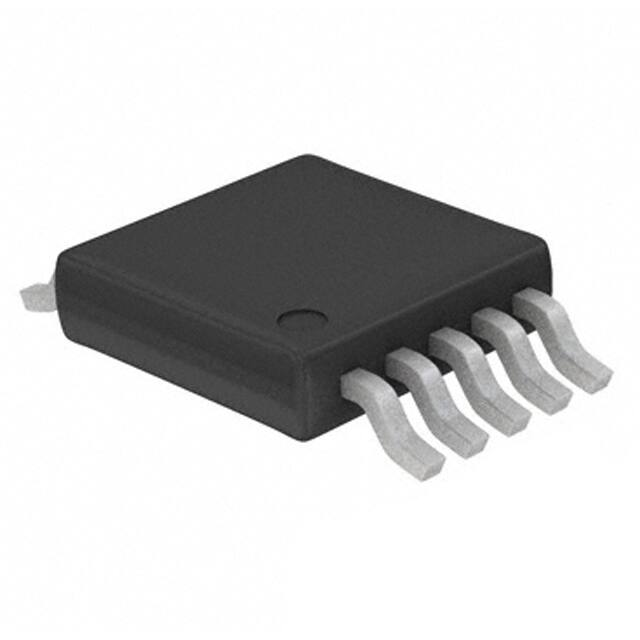
current. The RT8268 is available in the SOP-8 and
MSOP-10 (Exposed Pad) surface mount package.
z
z
z
z
z
z
z
z
z
z
Ordering Information
RT8268
Package Type
S : SOP-8
FP : MSOP-10 (Exposed Pad)
Lead Plating System
G : Green (Halogen Free and Pb Free)
Note :
Richtek products are :
`
Applications
z
z
z
z
Distributive Power Systems
Battery Charger
DSL Modems
Pre-regulator for Linear Regulators
Pin Configurations
(TOP VIEW)
RoHS compliant and compatible with the current requirements of IPC/JEDEC J-STD-020.
`
High Efficiency up to 95%
400kHz Fixed Switching Frequency
Stable with Low ESR Output Ceramic Capacitors
Programmable Soft-Start
Thermal Shutdown Protection
Cycle-By-Cycle Over Current Protection
RoHS Compliant and Halogen Free
Suitable for use in SnPb or Pb-free soldering processes.
Marking Information
For marking information, contact our sales representative
directly or through a Richtek distributor located in your
area.
NC
BOOT
NC
VIN
SW
10
2
3
4
5
9
GND
8
11 7
6
SS
EN
COMP
FB
GND
MSOP-10 (Exposed Pad)
8
SS
VIN
2
7
EN
SW
3
6
COMP
GND
4
5
FB
BOOT
SOP-8
DS8268-02 March 2011
www.richtek.com
1
�RT8268
Typical Application Circuit
VIN
4.75V to 24V
CIN
10µF/25V
BOOT
VIN
CBOOT
L1
15µH
10nF
RT8268
SW
Chip Enable
D1
B220A
EN
COUT
22µF/6.3V
FB
SS
CSS
10nF
R1
25.8k
CC
3.9nF
COMP
GND
VOUT
3.3V
RC
10k
R2
10k
CP
NC
Table 1. Recommended Component Selection
VOUT (V)
R1 (kΩ)
R2 (kΩ)
RC (kΩ)
CC (nF)
L1 (μH)
COU T (μF)
15
153
10
48.7
0.82
33
22
10
100
10
34
1.2
33
22
8
76.8
10
24
1.5
22
22
5
44.2
10
16
2.2
22
22
3.3
25.8
10
10
3.9
15
22
2.5
17
10
7.5
1.5
10
22
1.8
9.31
10
6.04
1.5
10
22
1.2
3
10
6.04
3.9
6.8
22
Function Block Diagram
VIN
VCC
Internal
Regulator
Oscillator
400kHz/120kHz
1µA
EN
10k
3V
VA VCC
Foldback
Control
+
1V
Shutdown
Comparator
VCC
0.5V
UV
Comparator
+
Current
Comparator
Logic
SW
GND
+
+EA
Gm = 920µA/V
0.92V
FB
www.richtek.com
2
VA
BOOT
+
10µA
SS
Current Sense
Slope Comp Amplifier
+
-
COMP
DS8268-02 March 2011
�RT8268
Functional Pin Description
Pin No.
Pin Name
Pin Function
PMSOP-10
SOP-8
1, 3
--
NC
No Internal Connection.
2
1
BOOT
High Side Gate Drive Bootstrap Input. BOOT supplies the drive for the
high side N-MOSFET switch. Connect a 10nF or greater capacitor
from SW to BOOT to power the high side switch.
4
2
VIN
Power Input. VIN supplies the power to the IC, as well as the
step-down converter switches. Bypass VIN to GND with a suitable
large capacitor to eliminate noise on the input to the IC.
5
3
SW
6,
11 (Exposed Pad)
4
GND
7
5
FB
8
6
COMP
9
7
EN
10
8
SS
DS8268-02 March 2011
Power Switching Output. SW is the switching node that supplies
power to the output. Connect the output LC filter from SW to the
output load. Note that a capacitor is required from SW to BOOT to
power the high side switch.
Ground. The exposed pad must be soldered to a large PCB and
connected to GND for maximum power dissipation.
Feedback Input. FB senses the output voltage to regulate said
voltage. The feedback reference voltage is 0.92V typically.
Compensation Node. COMP is used to compensate the regulation
control loop. Connect a series RC network from COMP to GND to
compensate the regulation control loop. In some cases, an additional
capacitor from COMP to GND is required.
Enable Input. EN is a digital input that turns the regulator on or off.
Drive EN higher than 1.4V to turn on the regulator, lower than 0.4V to
turn it off. If the EN pin is open, it will be pulled to high by internal
circuit.
Soft-Start Control Input. SS controls the soft start period. Connect a
capacitor from SS to GND to set the soft-start period. A 10nF
capacitor sets the soft-start period to 1ms.
www.richtek.com
3
�RT8268
Absolute Maximum Ratings
z
z
z
z
z
z
z
z
z
z
(Note 1)
Supply Voltage, VIN ----------------------------------------------------------------------------------------- −0.3V to 26V
Switching Voltage, SW ------------------------------------------------------------------------------------- −0.3V to (VIN + 0.3V)
BOOT Voltage ------------------------------------------------------------------------------------------------ (VSW − 0.3V) to (VSW + 6V)
All Other Voltage --------------------------------------------------------------------------------------------- −0.3V to 6V
Power Dissipation, PD @ TA = 25°C
SOP-8 ---------------------------------------------------------------------------------------------------------- 0.833W
MSOP-10 (Exposed Pad) ---------------------------------------------------------------------------------- 1.163W
Package Thermal Resistance (Note 2)
SOP-8, θJA ---------------------------------------------------------------------------------------------------- 120°C/W
MSOP-10 (Exposed Pad), θJA ---------------------------------------------------------------------------- 86°C/W
MSOP-10 (Exposed Pad), θJC ---------------------------------------------------------------------------- 30°C/W
Junction Temperature --------------------------------------------------------------------------------------- 150°C
Lead Temperature (Soldering, 10 sec.) ----------------------------------------------------------------- 260°C
Storage Temperature Range ------------------------------------------------------------------------------- −65°C to 150°C
ESD Susceptibility (Note 3)
HBM (Human Body Mode) --------------------------------------------------------------------------------- 2kV
MM (Machine Mode) ---------------------------------------------------------------------------------------- 200V
Recommended Operating Conditions
z
z
z
z
(Note 4)
Supply Voltage, VIN ----------------------------------------------------------------------------------------- 4.75V to 24V
Enable Voltage, VEN ----------------------------------------------------------------------------------------- 0V to 5.5V
Junction Temperature Range ------------------------------------------------------------------------------ −40°C to 125°C
Ambient Temperature Range ------------------------------------------------------------------------------ −40°C to 85°C
Electrical Characteristics
(VIN = 12V, TA = 25°C unless otherwise specified)
Parameter
Symbol
Test Conditions
Min
Typ
Max
Unit
0.902
0.92
0.938
V
--
0.18
--
Ω
V EN = 0V, V SW = 0V
---
10
--
-10
Ω
μA
4.75V ≤ V IN ≤ 24V
Feedback Reference Voltage
VFB
High Side Switch-On Resistance
RDS(ON)1
Low Side Switch-On Resistance
Switch Leakage
RDS(ON)2
Current Limit
ILIM
Duty = 90%; VBOOT−SW = 4.8V
--
3
--
A
Current Sense Transconductance
GCS
Output Current to VCOMP
--
2.5
--
A/V
Error Amplifier Tansconductance
Gm
ΔIC = ±10μA
620
920
1220
μA/V
Oscillator Frequency
fSW
--
400
--
kHz
---
120
90
---
kHz
%
--
90
--
ns
3.8
4.2
4.5
V
--
250
--
mV
Short Circuit Oscillation Frequency
Maximum Duty Cycle
DMAX
Minimum On-Time
Under Voltage Lockout Threshold
Rising
Under Voltage Lockout Threshold
Hysteresis
tON
V FB = 0V
V FB = 0.8V
To be continued
www.richtek.com
4
DS8268-02 March 2011
�RT8268
Parameter
Symbol
Test Conditions
Min
Typ
Max
Unit
En input Low Voltage
--
--
0.4
V
En input High Voltage
1.4
--
5.5
V
---
1
22
-36
μA
μA
Enable Pull-up Current
Shutdown Current
ISHDN
VEN = 0V
VEN = 0V
Quiescent Current
IQ
VEN = 2V, VFB = 1V
--
0.6
1
mA
CSS = 10nF
--
1
--
ms
--
150
--
°C
Soft-Start Period
Thermal Shutdown
T SD
Note 1. Stresses listed as the above "Absolute Maximum Ratings" may cause permanent damage to the device. These are for
stress ratings. Functional operation of the device at these or any other conditions beyond those indicated in the
operational sections of the specifications is not implied. Exposure to absolute maximum rating conditions for extended
periods may remain possibility to affect device reliability.
Note 2. θJA is measured in the natural convection at TA = 25°C on a high effective thermal conductivity four layers test board of
JEDEC 51-7 thermal measurement standard. The case point of θJC is on the expose pad for MSOP-10 (Exposed Pad)
package.
Note 3. Devices are ESD sensitive. Handling precaution is recommended.
Note 4. The device is not guaranteed to function outside its operating conditions.
DS8268-02 March 2011
www.richtek.com
5
�RT8268
Typical Operating Characteristics
Efficiency vs. Load Current
Efficiency vs. Load Current
100
100
90
VIN = 12V
90
80
VIN = 24V
80
Efficiency (%)
Efficiency (%)
70
60
50
40
30
VIN = 12V
VIN = 24V
70
60
50
40
30
20
20
10
10
VOUT = 3.3V
VOUT = 5V
0
0
0
0.25
0.5
0.75
1
1.25
1.5
1.75
0
2
0.25
0.5
1
1.25
1.5
1.75
2
Output Voltage vs. Output Current
VREF vs. Temperature
3.295
0.925
3.293
Output Voltage (V)
0.930
0.920
V REF (V)
0.75
Load Current (A)
Load Current (A)
0.915
0.910
3.291
VIN = 24V
VIN = 12V
3.289
3.287
3.285
0.905
VIN = 12V, IOUT = 0A
3.283
0.900
-50
-25
0
25
50
75
100
0
125
0.25
0.5
Temperature (°C)
1
1.25
1.5
1.75
2
Current Limit vs. Duty Cycle
Quiescent Current vs. Temperature
0.75
4.7
0.70
4.2
Current Limit (A)
Quiescent Current (mA)
0.75
Load Current (A)
0.65
0.60
0.55
3.7
3.2
2.7
0.50
VIN = 12V
0.45
2.2
-50
-25
0
25
50
75
Temperature (°C)
www.richtek.com
6
100
125
0
10
20
30
40
50
60
70
80
90
100
Duty Cycle (%)
DS8268-02 March 2011
�RT8268
Switching Frequency vs. Temperature
Switching Frequency vs. Input Voltage
420
Switching Frequency (kHz)
Switching Frequency (kHz)
404
402
400
398
396
394
410
VIN = 12V
400
VIN = 23V
390
380
370
VOUT = 3.3V, IOUT = 0.3A
VOUT = 3.3V, IOUT = 0.3A
360
392
3
6
9
12
15
18
21
24
-50
-25
0
25
50
75
100
125
Temperature (°C)
Input Voltage (V)
Output Ripple Voltage
Output Voltage vs. Input Voltage
3.298
VOUT
(10mV/Div)
Output Voltage (V)
3.296
3.294
IOUT = 2A
IOUT = 0A
3.292
IOUT = 1A
3.290
VSW
(10V/Div)
3.288
IL1
(1A/Div)
3.286
VIN = 12V, VOUT = 3.3V, IOUT = 2A
3.284
3
6
9
12
15
18
21
Time (1μs/Div)
24
Input Voltage (V)
Load Transient Response
Load Transient Response
VOUT
(200mV/Div)
VOUT
(100mV/Div)
IOUT
(1A/Div)
IOUT
(1A/Div)
VIN = 12V, VOUT = 3.3V, IOUT = 0 to 2A
Time (100μs/Div)
DS8268-02 March 2011
VIN = 12V, VOUT = 3.3V, IOUT = 1A to 2A
Time (100μs/Div)
www.richtek.com
7
�RT8268
Power Off from EN
Power On from EN
VIN = 12V, VOUT = 3.3V, IOUT = 2A
VIN = 12V, VOUT = 3.3V, IOUT = 2A
VEN
(5V/Div)
VEN
(5V/Div)
VOUT
(1V/Div)
I IN
(500mA/Div)
VOUT
(1V/Div)
Time (250μs/Div)
www.richtek.com
8
Time (25μs/Div)
DS8268-02 March 2011
�RT8268
Application Information
The RT8268 is an asynchronous high voltage buck
converter that can support the input voltage range from
4.75V to 24V and the output current can be up to 2A.
Output Voltage Setting
The resistive divider allows the FB pin to sense the output
voltage as shown in Figure 1.
V OUT
FB
R2
GND
Figure 1. Output Voltage Setting
The output voltage is set by an external resistive divider
according to the following equation :
VOUT = VFB ⎛⎜ 1+ R1 ⎞⎟
⎝ R2 ⎠
Where VFB is the feedback reference voltage (0.92V typ.).
External Bootstrap Diode
Connect a 10nF low ESR ceramic capacitor between the
BOOT pin and SW pin. This capacitor provides the gate
driver voltage for the high side MOSFET.
It is recommended to add an external bootstrap diode
between an external 5V and the BOOT pin for efficiency
improvement when input voltage is lower than 5.5V or duty
ratio is higher than 65%. The bootstrap diode can be a
low cost one such as 1N4148 or BAT54.
The external 5V can be a 5V fixed input from system or a
5V output of the RT8268.
5V
BOOT
RT8268
The RT8268 contains an external soft-start clamp that
gradually raises the output voltage. The soft-start timming
can be programed by the external capacitor between SS
pin and GND. The chip provides a 10μA charge current for
the external capacitor. If 10nF capacitor is used to set the
soft-start and it’ s period will be 1ms (typ.).
Inductor Selection
R1
RT8268
Soft-Start
10nF
SW
Figure 2. External Bootstrap Diode
The inductor value and operating frequency determine the
ripple current according to a specific input and output
voltage. The ripple current ΔIL increases with higher VIN
and decreases with higher inductance.
V
V
ΔIL = ⎡⎢ OUT ⎤⎥ × ⎡⎢1− OUT ⎤⎥
VIN ⎦
⎣ f ×L ⎦ ⎣
Having a lower ripple current reduces not only the ESR
losses in the output capacitors but also the output voltage
ripple. High frequency with small ripple current can achieve
highest efficiency operation. However, it requires a large
inductor to achieve this goal.
For the ripple current selection, the value of ΔIL = 0.24(IMAX)
will be a reasonable starting point. The largest ripple current
occurs at the highest VIN. To guarantee that the ripple
current stays below the specified maximum, the inductor
value should be chosen according to the following
equation :
⎡ VOUT ⎤ ⎡
VOUT ⎤
L =⎢
⎥ × ⎢1− VIN(MAX) ⎥
f
×
Δ
I
L(MAX)
⎣
⎦ ⎣
⎦
Inductor Core Selection
The inductor type must be selected once the value for L
is known. Generally speaking, high efficiency converters
can not afford the core loss found in low cost powdered
iron cores. So, the more expensive ferrite or
mollypermalloy cores will be a better choice.
The selected inductance rather than the core size for a
fixed inductor value is the key for actual core loss. As the
inductance increases, core losses decrease. Unfortunately,
increase of the inductance requires more turns of wire
and therefore the copper losses will increase.
Ferrite designs are preferred at high switching frequency
due to the characteristics of very low core losses. So,
design goals can focus on the reduction of copper loss
and the saturation prevention.
DS8268-02 March 2011
www.richtek.com
9
�RT8268
Ferrite core material saturates “hard”, which means that
inductance collapses abruptly when the peak design
current is exceeded. The previous situation results in an
abrupt increase in inductor ripple current and consequent
output voltage ripple.
refer to table 3 for more detail.
Do not allow the core to saturate!
Loop stability can be checked by viewing the load transient
response as described in a later section.
Different core materials and shapes will change the size/
current and price/current relationship of an inductor.
Toroid or shielded pot cores in ferrite or permalloy materials
are small and do not radiate energy. However, they are
usually more expensive than the similar powdered iron
inductors. The rule for inductor choice mainly depends
on the price vs. size requirement and any radiated field/
EMI requirements.
Diode Selection
When the power switch turns off, the path for the current
is through the diode connected between the switch output
and ground. This forward biased diode must have a
minimum voltage drop and recovery times. Schottky diode
is recommended and it should be able to handle those
current. The reverse voltage rating of the diode should be
greater than the maximum input voltage, and current rating
should be greater than the maximum load current. For
more detail please refer to Table 4.
CIN and COUT Selection
The input capacitance, C IN, is needed to filter the
trapezoidal current at the source of the high side MOSFET.
To prevent large ripple current, a low ESR input capacitor
sized for the maximum RMS current should be used. The
RMS current is given by :
IRMS = IOUT(MAX)
VOUT
VIN
VIN
−1
VOUT
This formula has a maximum at VIN = 2VOUT, where
I RMS = I OUT /2. This simple worst-case condition is
commonly used for design because even significant
deviations do not offer much relief.
Choose a capacitor rated at a higher temperature than
required. Several capacitors may also be paralleled to
meet size or height requirements in the design.
For the input capacitor, a 10μF low ESR ceramic capacitor
is recommended. For the recommended capacitor, please
www.richtek.com
10
The selection of COUT is determined by the required ESR
to minimize voltage ripple.
Moreover, the amount of bulk capacitance is also a key
for COUT selection to ensure that the control loop is stable.
The output ripple, ΔVOUT , is determined by :
1
⎤
ΔVOUT ≤ ΔIL ⎡⎢ESR +
8fCOUT ⎦⎥
⎣
The output ripple will be highest at the maximum input
voltage since ΔIL increases with input voltage. Multiple
capacitors placed in parallel may be needed to meet the
ESR and RMS current handling requirement. Dry tantalum,
special polymer, aluminum electrolytic and ceramic
capacitors are all available in surface mount packages.
Special polymer capacitors offer very low ESR value.
However, it provides lower capacitance density than other
types. Although Tantalum capacitors have the highest
capacitance density, it is important to only use types that
pass the surge test for use in switching power supplies.
Aluminum electrolytic capacitors have significantly higher
ESR. However, it can be used in cost-sensitive applications
for ripple current rating and long term reliability
considerations. Ceramic capacitors have excellent low
ESR characteristics but can have a high voltage coefficient
and audible piezoelectric effects. The high Q of ceramic
capacitors with trace inductance can also lead to significant
ringing.
Higher values, lower cost ceramic capacitors are now
becoming available in smaller case sizes. Their high ripple
current, high voltage rating and low ESR make them ideal
for switching regulator applications. However, care must
be taken when these capacitors are used at input and
output. When a ceramic capacitor is used at the input
and the power is supplied by a wall adapter through long
wires, a load step at the output can induce ringing at the
input, VIN. At best, this ringing can couple to the output
and be mistaken as loop instability. At worst, a sudden
inrush of current through the long wires can potentially
cause a voltage spike at VIN large enough to damage the
part.
DS8268-02 March 2011
�RT8268
Checking Transient Response
1.2
PD(MAX) = ( TJ(MAX) - TA ) / θJA
Where T J(MAX) is the maximum operation junction
temperature, TA is the ambient temperature and the θJA is
the junction to ambient thermal resistance.
For recommended operating conditions specification of
RT8268, the maximum junction temperature is 125°C. The
junction to ambient thermal resistance θJA for MSOP-10
(Exposed Pad) package is 86°C/W and for SOP-8 is
120°C/W on the standard JEDEC 51-7 four-layers thermal
test board. The maximum power dissipation at TA = 25°C
can be calculated by following formula :
PD(MAX) = (125°C − 25°C) / (86°C/W) = 1.163W for
MSOP-10 (Exposed Pad)
PD(MAX) = (125°C − 25°C) / (120°C/W) = 0.833W for
SOP-8
1
SOP-8
0.9
MSOP-10 (Exposed Pad)
0.8
0.7
0.6
0.5
0.4
0.3
0.2
0.1
0
Thermal Considerations
The maximum power dissipation depends on the thermal
resistance of IC package, PCB layout, the rate of
surroundings airflow and temperature difference between
junction to ambient. The maximum power dissipation can
be calculated by following formula :
Four Layer PCB
1.1
Power Dissipation (W)
The regulator loop response can be checked by looking
at the load transient response. Switching regulators take
several cycles to respond to a step in load current. When
a load step occurs, VOUT immediately shifts by an amount
equal to ΔILOAD (ESR) also begins to charge or discharge
COUT generating a feedback error signal for the regulator
to return VOUT to its steady-state value. During this recovery
time, VOUT can be monitored for overshoot or ringing that
would indicate a stability problem.
0
25
50
75
100
125
Ambient Temperature (°C)
(°C)
Figure 3. Derating Curves for RT8268 Packages
Layout Consideration
Follow the PCB layout guidelines for optimal performance
of the RT8268.
`
Keep the traces of the main current paths as short and
wide as possible.
`
Put the input capacitor as close as possible to the device
pins (VIN and GND).
`
LX node is with high frequency voltage swing and should
be kept at small area. Keep sensitive components away
from the LX node to prevent stray capacitive noise pickup.
`
Place the feedback components to the FB pin as close
as possible.
`
The GND and Exposed Pad should be connected to a
strong ground plane for heat sinking and noise protection.
The maximum power dissipation depends on operating
ambient temperature for fixed T J(MAX) and thermal
resistance θJA. For RT8268 packages, the Figure 3 of
derating curves allows the designer to see the effect of
rising ambient temperature on the maximum power
dissipation allowed.
DS8268-02 March 2011
www.richtek.com
11
�RT8268
CS
SW
CB
V IN
C IN
Input capacitor must
be placed as close
to the IC as possible.
NC
BOOT
NC
VIN
D1 SW
C OUT
The feedback components
must be connected as close
to the device as possible.
CC
10
2
9
3
GND
8
4
11
7
5
6
SS
EN
COMP
FB
GND
RC
CP
R1
V OUT
R2
L1
SW should be connected to inductor by
V OUT wide and short trace. Keep sensitive
components away from this trace.
GND
Figure 4. PCB Layout Guide for MSOP-10 (Exposed Pad)
GND
V IN
SW
CS
CB
Input capacitor must
be placed as close to
the IC as possible.
C IN
BOOT
D1
The parallel distance
between COMP and
FB traces must be as
short as possible.
8
SS
VIN
2
7
EN
SW
3
6
COMP
5
FB
C OUT
4
GND
L1
The output capacitor
must be placed near V OUT
the RT8268.
SW should be connected to
inductor by wide and short trace.
Keep sensitive components away
from this trace.
CC
CP
RC
GND
V OUT
The resistor divider must be
connected as close to the
device as possible.
Figure 5. PCB Layout Guide for SOP-8
www.richtek.com
12
DS8268-02 March 2011
�RT8268
Table 2. Suggested Inductors for Typical Application Circuit
Component Supplier
Series
Dimensions (mm)
TDK
SLF12555T
12.5 x 12.5 x 5.5
TAIYO YUDEN
NR8040
8x8 x4
TDK
SLF12565T
12.5 x 12.5 x 6.5
Table 3. Suggested Capacitors for CIN and COUT
Location
Component Supplier
Part No.
Capacitance (μF)
Case Size
CIN
MURATA
GRM31CR61E106K
10
1206
CIN
TDK
C3225X5R1E106K
10
1206
CIN
TAIYO YUDEN
TMK316BJ106ML
10
1206
COUT
MURATA
GRM32ER61E226M
22
1210
COUT
TDK
C3225X5R0J226M
22
1210
COUT
TAIYO YUDEN
EMK325BJ226MM
22
1210
Table 4. Suggested Diode
Component Supplier
Series
VRRM (V)
IOUT (A)
Package
DIODES
B330A
30
3
SMA
DIODES
B220A
20
2
SMA
PANJIT
SK22
20
2
DO-214AA
PANJIT
SK23
30
2
DO-214AA
DS8268-02 March 2011
www.richtek.com
13
�RT8268
Outline Dimension
H
A
M
J
B
F
C
I
D
Dimensions In Millimeters
Dimensions In Inches
Symbol
Min
Max
Min
Max
A
4.801
5.004
0.189
0.197
B
3.810
3.988
0.150
0.157
C
1.346
1.753
0.053
0.069
D
0.330
0.508
0.013
0.020
F
1.194
1.346
0.047
0.053
H
0.170
0.254
0.007
0.010
I
0.050
0.254
0.002
0.010
J
5.791
6.200
0.228
0.244
M
0.400
1.270
0.016
0.050
8-Lead SOP Plastic Package
www.richtek.com
14
DS8268-02 March 2011
�RT8268
D
L
EXPOSED THERMAL PAD
(Bottom of Package)
U
E
V
E1
e
A2
A
A1
b
Dimensions In Millimeters
Dimensions In Inches
Symbol
Min
Max
Min
Max
A
0.810
1.100
0.032
0.043
A1
0.000
0.100
0.000
0.004
A2
0.750
0.950
0.030
0.037
b
0.170
0.270
0.007
0.011
D
2.900
3.100
0.114
0.122
e
0.500
0.020
E
4.800
5.000
0.189
0.197
E1
2.900
3.100
0.114
0.122
L
0.400
0.800
0.016
0.031
U
1.300
1.700
0.051
0.067
V
1.500
1.900
0.059
0.075
10-Lead MSOP (Exposed Pad) Plastic Package
Richtek Technology Corporation
Richtek Technology Corporation
Headquarter
Taipei Office (Marketing)
5F, No. 20, Taiyuen Street, Chupei City
5F, No. 95, Minchiuan Road, Hsintien City
Hsinchu, Taiwan, R.O.C.
Taipei County, Taiwan, R.O.C.
Tel: (8863)5526789 Fax: (8863)5526611
Tel: (8862)86672399 Fax: (8862)86672377
Email: marketing@richtek.com
Information that is provided by Richtek Technology Corporation is believed to be accurate and reliable. Richtek reserves the right to make any change in circuit
design, specification or other related things if necessary without notice at any time. No third party intellectual property infringement of the applications should be
guaranteed by users when integrating Richtek products into any application. No legal responsibility for any said applications is assumed by Richtek.
DS8268-02 March 2011
www.richtek.com
15
�