®
RT8287A
4A, 21V 500kHz Synchronous Step-Down Converter
General Description
Features
The RT8287A is a synchronous step-down regulator with
an internal power MOSFET. It achieves 4A of continuous
output current over a wide input supply range with excellent
load and line regulation. Current mode operation provides
fast transient response and eases loop stabilization.
z
4A Output Current
z
Adjustable Soft-Start
120mΩ
Ω/40mΩ
Ω Internal Power MOSFET Switch
Internal Compensation Minimizes External Parts
Count
Fixed 500kHz Frequency
Thermal Shutdown Protection
Cycle-by-Cycle Over Current Protection
Wide 4.5V to 21V Operating Input Range
Adjustable Output from 0.808V to 15V
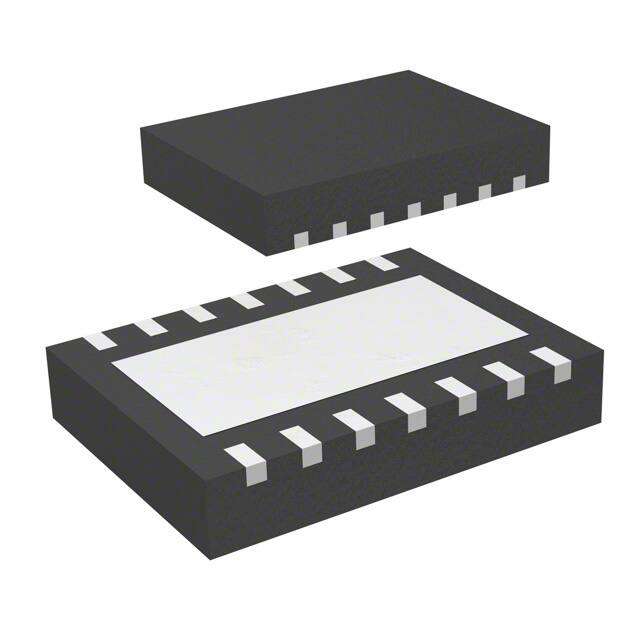
Small 14-Lead WDFN Package
RoHS Compliant and Halogen Free
Fault condition protection includes cycle-by-cycle current
limiting and thermal shutdown. An adjustable soft-start
reduces the stress on the input source at startup.
z
z
z
z
z
z
The RT8287A requires a minimal number of readily
available external components, providing a compact
solution.
Ordering Information
RT8287A
z
z
z
Applications
z
Package Type
QW : WDFN-14L 4x3 (W-Type)
Lead Plating System
Z : ECO (Ecological Element with
Halogen Free and Pb free)
Note :
z
z
z
Distributive Power Systems
Battery Charger
DSL Modems
Pre-Regulator for Linear Regulators
Pin Configurations
Richtek products are :
`
RoHS compliant and compatible with the current requirements of IPC/JEDEC J-STD-020.
`
Suitable for use in SnPb or Pb-free soldering processes.
Marking Information
01 : Product Code
01 YM
DNN
(TOP VIEW)
VIN
SW
SW
SW
SW
BOOT
EN
14
13
1
2
3
4
5
6
7
GND
15
12
11
10
9
8
AGND
GND
GND
VCC
SS
PGOOD
FB
WDFN-14L 4x3
YMDNN : Date Code
Copyright © 2012 Richtek Technology Corporation. All rights reserved.
DS8287A-03 June 2012
is a registered trademark of Richtek Technology Corporation.
www.richtek.com
1
�RT8287A
Typical Application Circuit
1
VIN
BOOT
VIN
CIN
22µF
RT8287A
SW
6
CBOOT
0.1µF
2, 3, 4, 5
L
VOUT
1.2V/4A
9 PGOOD
PGOOD
R3
100k
11
VCC
CC
0.1µF
SS 10
R1
RT
FB 8
COUT
CSS
47nF
R2
7 EN
ON/OFF
AGND GND
14
12, 13, 15 (Exposed Pad)
Table 1. Recommended Components Selection
VOUT (V)
5
3.3
2.5
1.8
1.5
1.2
1.05
R1 (kΩ)
75
75
75
5
5
5
5
R2 (kΩ)
14.46
24.32
35.82
4.07
5.84
10.31
16.69
RT (kΩ)
0
0
0
30
39
47
47
L (μH)
4.7
3.6
3.6
2
2
2
1.5
COUT (μF)
22 x 2
22 x 2
22 x 2
22 x 2
22 x 2
22 x 2
22 x 2
Function Pin Description
Pin No.
Pin Name
Pin Function
1
VIN
Supply Input. VIN supplies the power to the IC, as well as the step-down converter
switches. Drive VIN with a 4.5V to 21V power source. Bypass VIN to GND with a
suitably large capacitor to eliminate noise on the input to the IC.
2, 3, 4, 5
SW
Switch Node. SW is the switching node that supplies power to the output. Connect
the output LC filter from SW to the output load. Note that a capacitor is required
from SW to BOOT to power the high side switch.
6
BOOT
High Side Gate Drive Boost Input. BOOT supplies the drive for the high side
N-MOSFET switch. Connect a 100nF or greater capacitor from SW to BOOT to
power the high side switch.
7
EN
8
FB
9
PGOOD
10
SS
Chip Enable (Active High). For automatic start-up, connect the EN pin to VIN with a
100kΩ resistor.
Feedback Input. FB senses the output voltage to regulate said voltage. Drive FB
with a resistive voltage divider from the output voltage. The feedback threshold is
0.808V.
Power Good Output. The output of this pin is open-drain. Power good threshold is
90% low to high and 70% high to low of regulation value.
Soft-Start Control Input. SS controls the soft-start period. Connect a capacitor from
SS to GND to set the soft-start period.
Copyright © 2012 Richtek Technology Corporation. All rights reserved.
www.richtek.com
2
is a registered trademark of Richtek Technology Corporation.
DS8287A-03 June 2012
�RT8287A
Pin No.
Pin Name
11
Pin Function
Bias Supply. Decouple with 0.1μF to 0.22μF capacitor. The capacitance should be
no more than 0.22μF.
Ground. The exposed pad must be soldered to a large PCB and connected to GND
for maximum power dissipation.
VCC
12, 13
GND
15 (Exposed Pad)
14
AGND
Analog Ground. Connect this pin to the system ground in PCB layout.
Function Block Diagram
VIN
1.2V
EN
Shutdown
Comparator
+
Regulator
-
Current Sense
Amplifier
-
Ramp
Generator
+
VA
VA
5k
VC
-
1µA
3V
+
Oscillator
500kHz
BOOT
S
Lockout
Comparator
Q
+
1.7V
Driver
R
PWM
Comparator
VCC
PGOOD
+
SW
Reference
Error
+ Amplifier
+
-
-
FB
VC
30pF
GND
400k
10µA
SS
Copyright © 2012 Richtek Technology Corporation. All rights reserved.
DS8287A-03 June 2012
1pF
is a registered trademark of Richtek Technology Corporation.
www.richtek.com
3
�RT8287A
Absolute Maximum Ratings
z
z
z
z
z
z
z
z
z
z
(Note 1)
Supply Input Voltage, VIN ---------------------------------------------------------------------------------Switch Voltage, SW ----------------------------------------------------------------------------------------Boot Voltage, BOOT ----------------------------------------------------------------------------------------Other Pins -----------------------------------------------------------------------------------------------------Power Dissipation, PD @ TA = 25°C
WDFN-14L 4x3 -----------------------------------------------------------------------------------------------Package Thermal Resistance (Note 2)
WDFN-14L 4x3, θJA -----------------------------------------------------------------------------------------WDFN-14L 4x3, θJC -----------------------------------------------------------------------------------------Junction Temperature ---------------------------------------------------------------------------------------Lead Temperature (Soldering, 10 sec.) -----------------------------------------------------------------Storage Temperature Range ------------------------------------------------------------------------------ESD Susceptibility (Note 3)
HBM (Human Body Model) ---------------------------------------------------------------------------------
Recommended Operating Conditions
z
z
z
−0.3V to 26V
−0.3V to (VIN + 0.3V)
(SW − 0.3V) to (SW + 6V)
−0.3V to 6V
1.667W
60°C/W
7°C/W
150°C
260°C
−65°C to 150°C
2kV
(Note 4)
Supply Input Voltage, VIN ---------------------------------------------------------------------------------- 4.5V to 21V
Junction Temperature Range ------------------------------------------------------------------------------- −40°C to 125°C
Ambient Temperature Range ------------------------------------------------------------------------------- −40°C to 85°C
Electrical Characteristics
(VIN = 12V, TA = 25°C unless otherwise specified)
Parameter
Symbol
Test Conditions
Min
Typ
Max
Unit
Shutdown Current
ISHDN
VEN = 0
--
0
1
μA
Quiescent Current
IQ
VEN = 2V, VFB = 1V
--
0.7
--
mA
Upper Switch On Resistance
R DS(ON)1
--
120
--
mΩ
Lower Switch On Resistance
R DS(ON)2
--
40
--
mΩ
Switch Leakage
ILEAK
VEN = 0V, VSW = 0V or 12V
--
0
10
μA
Current Limit
ILIMIT
VBOOT − VSW = 4.8V
6.2
7
--
A
Oscillator Frequency
fSW
VFB = 0.75V
425
500
575
kHz
VFB = 0V
--
150
--
kHz
VFB = 0.8V
--
90
--
%
--
100
--
ns
0.82
V
nA
Short Circuit Frequency
Maximum Duty Cycle
D MAX
Minimum On Time
tON
Feedback Voltage
VFB
Feedback Current
IFB
--
10
50
Logic-High
VIH
2
--
5.5
Logic-Low
VIL
--
--
0.4
VEN = 2V
--
1
--
VEN = 0V
--
0
--
EN Threshold
Voltage
Enable Current
4.5V ≤ VIN ≤ 21V
Copyright © 2012 Richtek Technology Corporation. All rights reserved.
www.richtek.com
4
0.796 0.808
V
μA
is a registered trademark of Richtek Technology Corporation.
DS8287A-03 June 2012
�RT8287A
Parameter
Symbol
Min
Typ
Max
Unit
Power Good Rising Threshold
--
90
--
%
Power Good Falling Threshold
--
70
--
%
Power Good Delay
--
20
--
μs
--
--
0.4
V
--
10
--
nA
3.8
4
4.2
V
--
400
--
mV
--
5
--
V
ICC = 5mA
--
5
--
%
CSS = 47nF
--
4.7
--
ms
Power Good Sink Current
Capability
Test Conditions
Sink 4mA
Power Good Leakage Current
Under Voltage Lockout
Threshold
Under Voltage Lockout
Threshold Hysteresis
VUVLO
VIN Rising
ΔVUVLO
VCC Regulator
VCC Load Regulation
Soft-Start Period
tSS
Thermal Shutdown
TSD
--
150
--
°C
Thermal Shutdown Hysteresis
ΔTSD
--
30
--
°C
Note 1. Stresses beyond those listed “Absolute Maximum Ratings” may cause permanent damage to the device. These are
stress ratings only, and functional operation of the device at these or any other conditions beyond those indicated in
the operational sections of the specifications is not implied. Exposure to absolute maximum rating conditions may
affect device reliability.
Note 2. θJA is measured at TA = 25°C on a high effective thermal conductivity four-layer test board per JEDEC 51-7. θJC is
measured at the exposed pad of the package.
Note 3. Devices are ESD sensitive. Handling precaution is recommended.
Note 4. The device is not guaranteed to function outside its operating conditions.
Copyright © 2012 Richtek Technology Corporation. All rights reserved.
DS8287A-03 June 2012
is a registered trademark of Richtek Technology Corporation.
www.richtek.com
5
�RT8287A
Typical Operating Characteristics
Efficiency vs. Output Current
Reference Voltage vs. Input Voltage
100
0.830
90
VIN = 12V
0.825
Reference Voltage (V)
Efficiency (%)
80
VIN = 21V
70
60
50
40
30
20
0.820
0.815
0.810
0.805
0.800
0.795
10
VOUT = 1.22V, IOUT = 0A to 4A
0
0.790
0
0.5
1
1.5
2
2.5
3
3.5
4
4
6
8
10
Output Current (A)
14
16
18
20
22
Input Voltage (V)
Reference Voltage vs. Temperature
Output Voltage vs. Output Current
0.84
1.226
0.83
1.224
0.82
1.222
Output Voltage (V)
Reference Voltage (V)
12
0.81
0.80
0.79
0.78
1.220
1.218
1.216
1.214
0.77
1.212
0.76
1.210
VIN = 12V, VOUT = 1.22V, IOUT = 0A to 4A
-50
-25
0
25
50
75
100
0
125
0.5
1
1.5
Temperature (°C)
Switching Frequency vs. Input Voltage
2.5
3
3.5
4
Switching Frequency vs. Temperature
550
550
525
525
Switching Frequency (kHz)1
Switching Frequency (kHz)1
2
Output Current (A)
500
475
450
425
400
375
500
475
450
425
400
375
VOUT = 1.22V, IOUT = 0.8A
VIN = 12V, VOUT = 1.22V, IOUT = 1A
350
350
4
6
8
10
12
14
16
18
20
Input Voltage (V)
Copyright © 2012 Richtek Technology Corporation. All rights reserved.
www.richtek.com
6
22
-50
-25
0
25
50
75
100
125
Temperature (°C)
is a registered trademark of Richtek Technology Corporation.
DS8287A-03 June 2012
�RT8287A
Current Limit vs. Input Voltage
Current Limit vs. Temperature
12
11
10
Current Limit (A)
Current Limit (A)
10
8
6
4
9
8
7
6
5
2
4
VIN = 12V, VOUT = 1.22V
0
3
4
6
8
10
12
14
16
18
20
22
-50
-25
0
25
50
75
100
Input Voltage (V)
Temperature (°C)
Load Transient Response
Load Transient Response
VOUT
(200mV/Div)
VOUT
(200mV/Div)
IOUT
(2A/Div)
IOUT
(2A/Div)
VIN = 12V, VOUT = 1.22V, IOUT = 1A to 4A
VIN = 12V, VOUT = 1.22V, IOUT = 0A to 4A
Time (100μs/Div)
Time (100μs/Div)
Output Voltage Ripple
Output Voltage Ripple
VOUT
(50mV/Div)
VOUT
(50mV/Div)
VLX
(10V/Div)
VLX
(10V/Div)
IL
(2A/Div)
IL
(2A/Div)
VIN = 12V, IOUT = 1A
Time (1μs/Div)
Copyright © 2012 Richtek Technology Corporation. All rights reserved.
DS8287A-03 June 2012
125
VIN = 12V, IOUT = 4A
Time (1μs/Div)
is a registered trademark of Richtek Technology Corporation.
www.richtek.com
7
�RT8287A
Power Off from VIN
Power On from VIN
VIN
(10V/Div)
VIN
(10V/Div)
VOUT
(1V/Div)
VOUT
(1V/Div)
VPGOOD
(5V/Div)
IL
(5A/Div)
VPGOOD
(5V/Div)
IL
(5A/Div)
VIN = 12V, VOUT = 1.22V, IOUT = 4A
Time (5ms/Div)
Time (50ms/Div)
Power On from EN
Power Off from EN
VEN
(5V/Div)
VEN
(5V/Div)
VOUT
(1V/Div)
VOUT
(1V/Div)
VPGOOD
(5V/Div)
IL
(5A/Div)
VPGOOD
(5V/Div)
IL
(5A/Div)
VIN = 12V, VOUT = 1.22V, IOUT = 4A
Time (2.5ms/Div)
Copyright © 2012 Richtek Technology Corporation. All rights reserved.
www.richtek.com
8
VIN = 12V, VOUT = 1.22V, IOUT = 4A
VIN = 12V, VOUT = 1.22V, IOUT = 4A
Time (50μs/Div)
is a registered trademark of Richtek Technology Corporation.
DS8287A-03 June 2012
�RT8287A
Application Information
The IC is a synchronous high voltage buck converter that
can support the input voltage range from 4.5V to 21V and
the output current can be up to 4A.
Soft-Start
The output voltage is set by an external resistive divider
according to the following equation :
The IC contains an external soft-start clamp that gradually
raises the output voltage. The soft-start timing is
programmed by the external capacitor between SS pin
and GND. The chip provides an internal 10μA charge current
for the external capacitor. If 47nF capacitor is used to set
the soft-start, the period will be 4.7ms (typ.).
VOUT = VFB ⎛⎜ 1+ R1 ⎞⎟
⎝ R2 ⎠
Under Voltage Lockout Threshold
Output Voltage Setting
where VFB is the feedback reference voltage 0.808V
(typical).
The resistive divider allows the FB pin to sense a fraction
of the output voltage as shown in Figure 1.
VOUT
R1
FB
RT8287A
R2
GND
Figure 1. Output Voltage Setting
External Bootstrap Diode
Connect a 100nF low ESR ceramic capacitor between
the BOOT pin and SW pin as shown in Figure 2. This
capacitor provides the gate driver voltage for the high side
MOSFET. It is recommended to add an external bootstrap
diode between an external 5V and BOOT pin for efficiency
improvement when input voltage is lower than 5.5V or duty
ratio is higher than 65% .The bootstrap diode can be a
low cost one such as IN4148 or BAT54. The external 5V
can be a 5V fixed input from system or a 5V output of the
IC. Note that the external boot voltage must be lower than
5.5V.
5V
BOOT
RT8287A
100nF
SW
The IC includes an input Under Voltage Lockout Protection
(UVLO). If the input voltage exceeds the UVLO rising
threshold voltage (4.2V), the converter resets and prepares
the PWM for operation. If the input voltage falls below the
UVLO falling threshold voltage (3.8V) during normal
operation, the device stops switching. The UVLO rising
and falling threshold voltage includes a hysteresis to
prevent noise caused reset.
Chip Enable Operation
The EN pin is the chip enable input. Pulling the EN pin
low (2V,