RT8294
2A, 23V, 340kHz Synchronous Step-Down Converter
General Description
Features
The RT8294 is a high efficiency, monolithic synchronous
step-down DC/DC converter that can deliver up to 2A output
current from a 4.5V to 23V input supply. The RT8294's
current mode architecture and external compensation
allow the transient response to be optimized over a wide
range of loads and output capacitors. Cycle-by-cycle
current limit provides protection against shorted outputs
and soft-start eliminates input current surge during start
up. The RT8294 also provides under voltage protection
and thermal shutdown protection. The low current (< 3µA)
shutdown mode provides output disconnection, enabling
easy power management in battery-powered systems. The
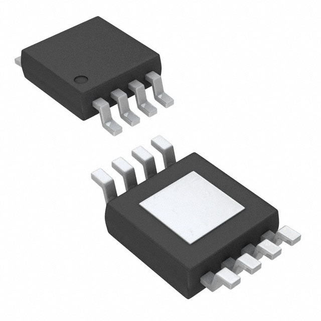
RT8294 is available in SOP-8 and SOP-8 (Exposed Pad)
packages.
l
l
l
l
l
l
l
l
l
l
l
l
l
l
l
±1.5% High Accuracy Feedback Voltage
Input Voltage Range : 4.5V to 23V
2A Output Current
Integrated N-MOSFETs
Current Mode Control
340kHz Fixed Frequency Operation
Output Adjustable Voltage Range : 0.923V to 20V
Efficiency Up to 95%
Programmable Soft-Start
Stable with Low ESR Ceramic Output Capacitors
Cycle-by Cycle Over Current Protection
Input Under Voltage Lockout
Output Under Voltage Protection
Thermal Shutdown Protection
RoHS Compliant and Halogen Free
Ordering Information
Applications
RT8294
Package Type
S : SOP-8
SP: SOP-8(Exposed Pad-Option 1)
Lead Plating System
G : Green (Halogen Free and Pb Free)
Z : ECO (Ecological Element with
Halogen Free and Pb free)
Note :
Richtek products are :
}
l
l
l
l
l
l
Wireless AP/Router
Set-Top-Box
Industrial and Commercial Low Power Systems
LCD Monitors and TVs
Green Electronics/Appliances
Point of Load Regulation of High-Performance DSPs
Pin Configurations
(TOP VIEW)
RoHS compliant and compatible with the current requirements of IPC/JEDEC J-STD-020.
}
Suitable for use in SnPb or Pb-free soldering processes.
BOOT
VIN
SW
GND
8
SS
2
7
EN
3
6
COMP
4
5
FB
8
SS
SOP-8
BOOT
VIN
SW
GND
2
3
GND
7
EN
6
COMP
5
FB
9
4
SOP-8 (Exposed Pad)
DS8294-02 March 2011
www.richtek.com
1
�RT8294
Marking Information
RT8294GS
RT8294GSP
RT8294GSP : Product Number
RT8294GS : Product Number
RT8294
GSYMDNN
RT8294
GSPYMDNN
YMDNN : Date Code
YMDNN : Date Code
RT8294ZSP
RT8294ZSP : Product Number
RT8294
ZSPYMDNN
YMDNN : Date Code
Typical Application Circuit
VIN
4.5V to 23V
2
CIN
10µF
VIN
BOOT
RT8294
SW
REN 100k
CSS
0.1µF
1
7 EN
8 SS
4, 9 (Exposed Pad)
GND
3
CBOOT
L
10nF 10µH
R1
26.1k
FB 5
COMP
6
CC
3.3nF
RC
13k
VOUT
3.3V/2A
COUT
22µF x 2
R2
10k
CP
Open
Table 1. Recommended Component Selection
VOUT (V) R1 (kΩ) R2 (kΩ) RC (kΩ) C C (nF) L (µH)
8
76.8
10
27
3.3
22
5
45.3
10
20
3.3
15
3.3
26.1
10
13
3.3
10
2.5
16.9
10
9.1
3.3
6.8
1.8
9.53
10
5.6
3.3
4.7
1.2
3
10
3.6
3.3
3.6
www.richtek.com
2
COUT (µF)
22 x 2
22 x 2
22 x 2
22 x 2
22 x 2
22 x 2
DS8294-02 March 2011
�RT8294
Functional Pin Description
Pin No.
Pin Name
Pin Function
SOP-8
SOP-8
(Exposed Pad)
1
1
BOOT
Bootstrap for High Side Gate Driver. Connect a 10nF or greater
ceramic capacitor from BOOT to SW pins.
2
2
VIN
Input Supply Voltage, 4.5V to 23V. Must bypass with a suitably large
ceramic capacitor.
3
3
SW
4,
GND
9 (Exposed Pad)
4
5
5
FB
6
6
COMP
Phase Node. Connect this pin to external L-C filter.
Ground. The exposed pad must be soldered to a large PCB and
connected to GND for maximum power dissipation.
Feedback Input Pin. This pin is connected to the converter output. It
is used to set the output of the converter to regulate to the desired
value via an internal resistive voltage divider. For an adjustable
output, an external resistive voltage divider is connected to this pin.
Compensation Node. COMP is used to compensate the regulation
control loop. Connect a series RC network from COMP to GND. In
some cases, an additional capacitor from COMP to GND is required.
7
7
EN
Enable Input pin. A logic high enables the converter; a logic low
forces the RT8294 into shutdown mode reducing the supply current
to less than 3µA. Attach this pin to VIN with a 100kΩ pull up resistor
for automatic startup.
8
8
SS
Soft-Start Control Input. SS controls the soft-start period. Connect a
capacitor from SS to GND to set the soft-start period. A 0.1µF
capacitor sets the soft-start period to 15.5ms .
Function Block Diagram
VIN
Internal
Regulator
Oscillator
Slope Comp
Shutdown
Comparator VA VCC
1.2V
+
Foldback
Control
-
EN
5k
+
UV
Comparator
VA
0.5V
Lockout
Comparator
+
2.7V
3V
Current Sense
Amplifier
+
-
BOOT
S
+
R
Current
Comparator
VCC
Q
130m Ω
SW
Q
130m Ω
GND
6µA
SS
0.923V
FB
DS8294-02 March 2011
+
+
Error Amp
COMP
www.richtek.com
3
�RT8294
Absolute Maximum Ratings
(Note 1)
Supply Voltage, VIN ---------------------------------------------------------------------------------------------Input Voltage, SW -----------------------------------------------------------------------------------------------l VBOOT − VSW ------------------------------------------------------------------------------------------------------l Other Pins Voltages ---------------------------------------------------------------------------------------------l Power Dissipation, PD @ TA = 25°C
SOP-8 ---------------------------------------------------------------------------------------------------------------SOP-8 (Exposed Pad) -------------------------------------------------------------------------------------------l Package Thermal Resistance (Note 2)
SOP-8, θJA ---------------------------------------------------------------------------------------------------------SOP-8 (Exposed Pad), θJA -------------------------------------------------------------------------------------SOP-8 (Exposed Pad), θJC -------------------------------------------------------------------------------------l Junction Temperature -------------------------------------------------------------------------------------------l Lead Temperature (Soldering, 10 sec.) ----------------------------------------------------------------------l Storage Temperature Range -----------------------------------------------------------------------------------l ESD Susceptibility (Note 3)
HBM (Human Body Mode) -------------------------------------------------------------------------------------MM (Machine Mode) --------------------------------------------------------------------------------------------l
l
Recommended Operating Conditions
l
l
l
−0.3V to 25V
−0.3V to (VIN + 0.3V)
−0.3V to 6V
−0.3V to 6V
1.111W
1.333W
90°C/W
75°C
15°C
150°C
260°C
−65°C to 150°C
2kV
200V
(Note 4)
Supply Voltage, VIN ---------------------------------------------------------------------------------------------- 4.5V to 23V
Junction Temperature Range ----------------------------------------------------------------------------------- −40°C to 125°C
Ambient Temperature Range ----------------------------------------------------------------------------------- −40°C to 85°C
Electrical Characteristics
(VIN = 12V, TA = 25°C unless otherwise specified)
Parameter
Symbol
Shutdown Supply Current
Test Conditions
Min
Typ
Max
Unit
VEN = 0V
--
0.5
3
µA
Supply Current
ICC
VEN = 3 V, VFB = 1V
--
0.8
1.2
mA
Feedback Voltage
VFB
4.5V ≦ VIN ≦ 23V
0.909
0.923
0.937
V
--
940
--
µA/V
Error Amplifier Transconductance GEA
ΔIC = ± 10µA
High-Side Switch-On Resistance
RDS(ON)1
--
130
--
mΩ
Low-Side Switch-On Resistance
RDS(ON)2
--
130
--
mΩ
High-Side Switch Leakage Current
VEN = 0V, VSW = 0V
--
0
10
µA
Upper Switch Current Limit
Min.Duty Cycle, VBOOT−SW = 4.8V
--
4.3
--
A
Low Switch Current Limit
COMP to Current Sense
Transconductance
Oscillator Frequency
From Drain to Source
--
1.3
--
A
GCS
--
4
--
A/V
fOSC1
300
340
380
kHz
Short Circuit Oscillation
Frequency
fOSC2
VFB = 0V
--
100
--
kHz
DMAX
tON
VFB = 0.7V
--
93
--
%
--
100
--
ns
Maximum Duty Cycle
Minimum On-Time
To be continued
www.richtek.com
4
DS8294-02 March 2011
�RT8294
Parameter
EN Input Threshold
Voltage
Symbol
Test Conditions
Min
Typ
Max
Unit
Logic High
VIH
2.7
--
5.5
Logic Low
VIL
--
--
0.4
3.8
4.2
4.5
V
--
320
--
mV
VIN Rising
V
Input Under Voltage Lockout Threshold
VUVLO
Input Under Voltage Lockout Hysteresis
∆VUVLO
Soft-Start Current
ISS
VSS = 0V
--
6
--
µA
Soft-Start Period
tSS
C SS = 0.1µF
--
15.5
--
ms
Thermal Shutdown
TSD
--
150
--
°C
Note 1. Stresses listed as the above "Absolute Maximum Ratings" may cause permanent damage to the device. These are for
stress ratings. Functional operation of the device at these or any other conditions beyond those indicated in the
operational sections of the specifications is not implied. Exposure to absolute maximum rating conditions for extended
periods may remain possibility to affect device reliability.
Note 2. θJA is measured in natural convection at TA = 25°C on a high effective thermal conductivity four-layer test board, of
JEDEC 51-7 thermal measurement standard. The measurement case position of θJC is on the exposed pad of the
package.
Note 3. Devices are ESD sensitive. Handling precaution is recommended.
Note 4. The device is not guaranteed to function outside its operating conditions..
DS8294-02 March 2011
www.richtek.com
5
�RT8294
Typical Operating Characteristics
Efficiency vs. Output Current
Reference Voltage vs. Input Voltage
100
0.940
Efficiency (%)
80
Reference Voltage (V)
90
VIN = 4.5V
VIN = 12V
VIN = 23V
70
60
50
40
30
20
0.935
0.930
0.925
0.920
0.915
0.910
0.905
10
VOUT = 3.3V
0
0.900
0
0.25
0.5
0.75
1
1.25
1.5
1.75
2
4
6
8
10
Output Current (A)
Reference Voltage vs. Temperature
16
18
20
22
24
Output Voltage vs. Output Current
3.35
0.935
3.34
0.930
Output Voltage (V)
Reference Voltage (V)
14
3.36
0.940
0.925
0.920
0.915
0.910
3.33
3.32
3.31
3.30
VIN = 4.5V
VIN = 12V
VIN = 23V
3.29
3.28
3.27
3.26
0.905
3.25
0.900
VOUT = 3.3V
3.24
-50
-25
0
25
50
75
100
0
125
0.2
0.4
0.6
Temperature (°C)
0.8
1
1.2
1.4
1.6
1.8
2
Output Current (A)
Frequency vs. Input Voltage
Frequency vs. Temperature
380
380
370
370
360
360
Frequency (kHz)1
Frequency (kHz)1
12
Input Voltage (V)
350
340
330
320
350
340
330
320
310
310
VOUT = 3.3V, VIN = 12V, IOUT = 0A
VOUT = 3.3V, IOUT = 0A
300
300
4
6
8
10
12
14
16
18
Input Voltage (V)
www.richtek.com
6
20
22
24
-50
-25
0
25
50
75
100
125
Temperature (°C)
DS8294-02 March 2011
�RT8294
Current Limit vs. Temperature
Load Transient Response
6.0
Current Limit (A)
5.5
VOUT
(100mV/Div)
5.0
4.5
4.0
IOUT
(1A/Div)
3.5
VIN = 12V, VOUT = 3.3V
VIN = 12V, VOUT = 3.3V, IOUT = 0A to 2A
3.0
-50
-25
0
25
50
75
100
Time (100μs/Div)
125
Temprature (°C)
Load Transient Response
Switching
VOUT
(10mV/Div)
VOUT
(100mV/Div)
IL
(1A/Div)
VSW
(10V/Div)
IOUT
(1A/Div)
VIN = 12V, VOUT = 3.3V, IOUT = 1A to 2A
VIN = 12V, VOUT = 3.3V, IOUT = 2A
Time (100μs/Div)
Time (1μs/Div)
Power On from VIN
Power Off from VIN
VIN
(5V/Div)
VOUT
(2V/Div)
VIN
(5V/Div)
VOUT
(2V/Div)
IL
(1A/Div)
VIN = 12V, VOUT = 3.3V, IOUT = 2A
Time (10ms/Div)
DS8294-02 March 2011
IL
(1A/Div)
VIN = 12V, VOUT = 3.3V, IOUT = 2A
Time (10ms/Div)
www.richtek.com
7
�RT8294
Power On from EN
Power Off from EN
VEN
(2V/Div)
VEN
(2V/Div)
VOUT
(2V/Div)
VOUT
(2V/Div)
IOUT
(2A/Div)
IOUT
(2A/Div)
VIN = 12V, VOUT = 3.3V, IOUT = 2A
Time (10ms/Div)
www.richtek.com
8
VIN = 12V, VOUT = 3.3V, IOUT = 2A
Time (10ms/Div)
DS8294-02 March 2011
�RT8294
Application Information
The RT8294 is a synchronous high voltage buck converter
that can support the input voltage range from 4.5V to 23V
and the output current can be up to 2A.
Output Voltage Setting
The resistive voltage divider allows the FB pin to sense
the output voltage as shown in Figure 1.
Soft-Start
The RT8294 contains an external soft-start clamp that
gradually raises the output voltage. The soft-start timing
can be programmed by the external capacitor between
SS pin and GND. The chip provides a 6µA charge current
for the external capacitor. If 0.1µF capacitor is used to
set the soft-start, the period will be 15.5ms (typ.).
VOUT
Chip Enable Operation
R1
FB
RT8294
R2
GND
Figure 1. Output Voltage Setting
The output voltage is set by an external resistive voltage
divider according to the following equation :
VOUT = VFB 1 + R1
R2
where VFB is the feedback reference voltage 0.923V (typ.).
External Bootstrap Diode
Connect a 10nF low ESR ceramic capacitor between the
BOOT pin and SW pin. This capacitor provides the gate
driver voltage for the high side MOSFET.
It is recommended to add an external bootstrap diode
between an external 5V and BOOT pin for efficiency
improvement when input voltage is lower than 5.5V or duty
ratio is higher than 65% .The bootstrap diode can be a
low cost one such as IN4148 or BAT54. The external 5V
can be a 5V fixed input from system or a 5V output of the
RT8294. Note that the external boot voltage must be lower
than 5.5V
The EN pin is the chip enable input. Pulling the EN pin
low ( 2.7V, < 5.5V) will turn on
the device again. For external timing control (e.g.RC),
the EN pin can also be externally pulled high by adding a
REN* resistor and CEN* capacitor from the VIN pin
(see Figure 5).
An external MOSFET can be added to implement digital
control on the EN pin when no system voltage above 2.5V
is available, as shown in Figure 3. In this case, a 100kΩ
pull-up resistor, REN, is connected between VIN and the
EN pin. MOSFET Q1 will be under logic control to pull
down the EN pin.
2 VIN
VIN
REN
100k
Chip Enable
CIN
BOOT
1
CBOOT
RT8294
7 EN
VOUT
L
SW 3
R1
Q1
8 SS
CSS
4,
9 (Exposed Pad)
GND
COUT
FB 5
COMP
6
CC
RC
R2
CP
Figure 3. Enable Control Circuit for Logic Control with
Low Voltage
5V
BOOT
RT8294
10nF
SW
Figure 2. External Bootstrap Diode
DS8294-02 March 2011
To prevent enabling circuit when VIN is smaller than the
VOUT target value, a resistive voltage divider can be placed
between the input voltage and ground and connected to
the EN pin to adjust IC lockout threshold, as shown in
Figure 4. For example, if an 8V output voltage is regulated
from a 12V input voltage, the resistor, REN2, can be
selected to set input lockout threshold larger than 8V.
www.richtek.com
9
�RT8294
2
VIN
12V
REN1
100k
CIN
10µF
BOOT
VIN
1
CBOOT
L
RT8294
7 EN
SW
3
VOUT
8V
R1
REN2
8 SS
CSS
4,
9 (Exposed Pad)
GND
COUT
FB 5
COMP
6
CC
RC
R2
CP
Figure 4. The Resistors can be Selected to Set IC
Lockout Threshold
Hiccup Mode
For the RT8294, Hiccup Mode Under Voltage Protection
(UVP) is provided. When the FB voltage, VFB, drops below
0.5V, the UVP function will be triggered and the RT8294
will shut down for a period of time and then recover
automatically. The Hiccup Mode UVP can reduce input
current in short circuit conditions.
Inductor Selection
The inductor value and operating frequency determine the
ripple current according to a specific input and output
voltage. The ripple current ∆IL increases with higher VIN
and decreases with higher inductance.
V
V
∆IL = OUT × 1 − OUT
VIN
f ×L
Having a lower ripple current reduces not only the ESR
losses in the output capacitors but also the output voltage
ripple. High frequency with small ripple current can achieve
highest efficiency operation. However, it requires a large
inductor to achieve this goal.
Table 2. Suggested Inductors for Typical
Application Circuit
Component
Supplier
Series
Dimensions
(mm)
TDK
VLF10045
10 x 9.7 x 4.5
TDK
TAIYO
YUDEN
SLF12565
12.5 x 12.5 x 6.5
NR8040
8x8x4
CIN and COUT Selection
The input capacitance, C IN, is needed to filter the
trapezoidal current at the source of the high side MOSFET.
To prevent large ripple current, a low ESR input capacitor
sized for the maximum RMS current should be used. The
RMS current is given by :
V
IRMS = IOUT(MAX) OUT
VIN
VIN
−1
VOUT
This formula has a maximum at VIN = 2VOUT , where
IRMS = I OUT / 2. This simple worst case condition is
commonly used for design because even significant
deviations do not offer much relief.
Choose a capacitor rated at a higher temperature than
required. Several capacitors may also be paralleled to
meet size or height requirements in the design.
For the input capacitor, one 10µF low ESR ceramic
capacitors are recommended. For the recommended
capacitor, please refer to table 3 for more detail.
The selection of COUT is determined by the required ESR
to minimize voltage ripple.
Moreover, the amount of bulk capacitance is also a key
for COUT selection to ensure that the control loop is stable.
Loop stability can be checked by viewing the load transient
response as described in a later section.
For the ripple current selection, the value of ∆IL = 0.24(IMAX)
will be a reasonable starting point. The largest ripple
current occurs at the highest VIN. To guarantee that the
ripple current stays below the specified maximum, the
inductor value should be chosen according to the following
equation :
VOUT
VOUT
L =
× 1− VIN(MAX)
f
×
∆
I
L(MAX)
The output ripple will be highest at the maximum input
The inductor's current rating (caused a 40°C temperature
rising from 25°C ambient) should be greater than the
maximum load current and its saturation current should
be greater than the short circuit peak current limit. Please
see Table 2 for the inductor selection reference.
voltage since ∆IL increases with input voltage. Multiple
capacitors placed in parallel may be needed to meet the
ESR and RMS current handling requirement. Dry tantalum,
special polymer, aluminum electrolytic and ceramic
capacitors are all av ai labl e in surf ace mount
www.richtek.com
10
The output ripple, ∆VOUT , is determined by :
1
∆VOUT ≤ ∆IL ESR +
8fCOUT
DS8294-02 March 2011
�RT8294
Checking Transient Response
packages. Special polymer capacitors offer very low ESR
value. However, it provides lower capacitance density than
other types. Although Tantalum capacitors have the highest
capacitance density, it is important to only use types that
pass the surge test for use in switching power supplies.
Aluminum electrolytic capacitors have significantly higher
ESR. However, it can be used in cost sensitive applications
for ripple current rating and long term reliability
considerations. Ceramic capacitors have excellent low
ESR characteristics but can have a high voltage coefficient
and audible piezoelectric effects. The high Q of ceramic
capacitors with trace inductance can also lead to significant
ringing.
The regulator loop response can be checked by looking
at the load transient response. Switching regulators take
several cycles to respond to a step in load current. When
a load step occurs, VOUT immediately shifts by an amount
equal to ∆ILOAD (ESR) and COUT also begins to be charge
or discharged to generate a feedback error signal for the
regulator to return VOUT to its steady-state value. During
this recovery time, VOUT can be monitored for overshoot or
ringing that would indicate a stability problem.
EMI Consideration
Since parasitic inductance and capacitance effects in PCB
circuitry would cause a spike voltage on SW pin when
high side MOSFET is turned-on/off, this spike voltage on
SW may impact on EMI performance in the system. In
order to enhance EMI performance, there are two methods
to suppress the spike voltage. One way is by placing an
R-C snubber between SW and GND and locating them as
close as possible to the SW pin (see Figure 5). Another
method is by adding a resistor in series with the bootstrap
capacitor, CBOOT , but this method will decrease the driving
capability to the high side MOSFET. It is strongly
recommended to reserve the R-C snubber during PCB
layout for EMI improvement. Moreover, reducing the SW
trace area and keeping the main power in a small loop will
be helpful on EMI performance. For detailed PCB layout
guide, please refer to the section Layout Considerations.
Higher values, lower cost ceramic capacitors are now
becoming available in smaller case sizes. Their high ripple
current, high voltage rating and low ESR make them ideal
for switching regulator applications. However, care must
be taken when these capacitors are used at input and
output. When a ceramic capacitor is used at the input
and the power is supplied by a wall adapter through long
wires, a load step at the output can induce ringing at the
input, VIN. At best, this ringing can couple to the output
and be mistaken as loop instability. At worst, a sudden
inrush of current through the long wires can potentially
cause a voltage spike at VIN large enough to damage the
part.
2
VIN
4.5V to 23V
REN*
Chip Enable
CIN
10µF
VIN
BOOT
1
CBOOT
L
10nF 10µH
RT8294
7 EN
SW
3
RS*
CEN*
8 SS
C SS
4,
0.1µF Exposed Pad(9)
GND
* : Optional
RBOOT*
VOUT
3.3V/2A
R1
26.1k
CS*
COUT
22µFx2
FB 5
COMP
6
CC
3.3nF
RC
13k
R2
10k
CP
NC
Figure 5. Reference Circuit with Snubber and Enable Timing Control
DS8294-02 March 2011
www.richtek.com
11
�RT8294
Thermal Considerations
For continuous operation, do not exceed absolute
maximum operation junction temperature 125°C. The
maximum power dissipation depends on the thermal
resistance of IC package, PCB layout, the rate of
surroundings airflow and temperature difference between
junctions to ambient. The maximum power dissipation can
be calculated by following formula :
PD(MAX) = (TJ(MAX) − TA) / θJA
6.b) reduces the θJA to 64°C/W. Even further, increasing
the copper area of pad to 70mm2 (Figure 6.e) reduces the
θJA to 49°C/W.
The maximum power dissipation depends on operating
ambient temperature for fixed T J(MAX) and thermal
resistance θJA. For RT8294 packages, the of de-rating
curves in Figure 7 allow the designer to see the effect of
rising ambient temperature on the maximum power
dissipation allowed.
where T J(MAX) is the maximum operation junction
temperature, TA is the ambient temperature and the θJA
is the junction to ambient thermal resistance.
P D(MAX) = (125°C − 25°C) / (75°C/W ) = 1. 33W
(min. copper area PCB layout with SOP-8 Exposed Pad)
Four-Layer PCB
2.0
Power Dissipation (W)
For recommended operating conditions specification of
RT8294, the maximum junction temperature is 125°C. The
junction to ambient thermal resistance θJA is layout
dependent. For SOP-8 (Exposed Pad) package, the
thermal resistance θJA is 75°C/W on the standard JEDEC
51-7 four layers thermal test board. For SOP-8 package,
the thermal resistance θJA is 90°C/W on the standard
JEDEC 51-7 four layers thermal test board. The maximum
power dissipation at TA = 25°C can be calculated by
following formula :
2.2
Copper Area
70mm2
50mm2
30mm2
10mm2
Min.Layout
SOP-8
1.8
1.6
1.4
1.2
1.0
0.8
0.6
0.4
0.2
0.0
0
25
50
75
100
125
Ambient Temperature (°C)
Figure 7. Derating Curves for RT8294 Package
P D(MAX) = (125°C − 25°C) / (49°C/W ) = 2. 04W
(70mm2 copper area PCB layout with SOP-8 Exposed
Pad)
P D(MAX) = (125°C − 25°C) / (90°C/W ) = 1. 11W
(min. copper area PCB layout with SOP-8)
The thermal resistance θJA of SOP-8 (Exposed Pad) is
determined by the package architecture design and the
PCB layout design. However, the package architecture
design had been designed. If possible, it's useful to increase
thermal performance by the PCB layout copper design.
The thermal resistance θJA can be decreased by adding
copper area under the exposed pad of SOP-8 (Exposed
Pad) package.
As shown in Figure 6, the amount of copper area to which
the SOP-8 (Exposed Pad) is mounted affects thermal
(a) Copper Area = (2.3 x 2.3) mm2, θJA = 75°C/W
(b) Copper Area = 10mm2, θJA = 64°C/W
performance. When mounted to the standard SOP-8
(Exposed Pad) pad (Figure 6.a), θJA is 75°C/W. Adding
copper area of pad under the SOP-8 (Exposed Pad) (Figure
www.richtek.com
12
DS8294-02 March 2011
�RT8294
Layout Considerations
For best performance of the RT8294, the following layout
guidelines must be strictly followed.
(c) Copper Area = 30mm2 , θJA = 54°C/W
}
Input capacitor must be placed as close to the IC as
possible.
}
SW should be connected to inductor by wide and short
trace. Keep sensitive components away from this trace.
}
The feedback components must be connected as close
to the device as possible
The feedback components
must be connected as close
to the device as possible.
Input capacitor must be placed
as close to the IC as possible.
SW GND
VIN
GND
CSS
(d) Copper Area = 50mm2 , θJA = 51°C/W
CIN
BOOT
RS CS
VIN
2
SW
GND
3
GND
SS
7
EN
6
COMP
5
FB
9
4
COUT
VOUT
CC
8
L1
SW should be connected to inductor by
wide and short trace. Keep sensitive
components away from this trace.
REN VIN
CP
RC
R1
R2
VOUT
GND
Figure 8. PCB Layout Guide
(e) Copper Area = 70mm2 , θJA = 49°C/W
Figure 6. Thermal Resistance vs. Copper Area Layout
Design
Table 3. Suggested Capacitors for CIN and COUT
Location
Component Supplier
Part No.
Capacitance (μF)
Case Size
CIN
MURATA
GRM31CR61E106K
10
1206
CIN
TDK
C3225X5R1E106K
10
1206
CIN
TAIYO YUDEN
TMK316BJ106ML
10
1206
COUT
MURATA
GRM31CR60J476M
47
1206
COUT
TDK
C3225X5R0J476M
47
1210
COUT
MURATA
GRM32ER71C226M
22
1210
COUT
TDK
C3225X5R1C22M
22
1210
DS8294-02 March 2011
www.richtek.com
13
�RT8294
Outline Dimension
H
A
M
J
B
F
C
I
D
Dimensions In Millimeters
Dimensions In Inches
Symbol
Min
Max
Min
Max
A
4.801
5.004
0.189
0.197
B
3.810
3.988
0.150
0.157
C
1.346
1.753
0.053
0.069
D
0.330
0.508
0.013
0.020
F
1.194
1.346
0.047
0.053
H
0.170
0.254
0.007
0.010
I
0.050
0.254
0.002
0.010
J
5.791
6.200
0.228
0.244
M
0.400
1.270
0.016
0.050
8-Lead SOP Plastic Package
www.richtek.com
14
DS8294-02 March 2011
�RT8294
H
A
M
EXPOSED THERMAL PAD
(Bottom of Package)
Y
J
X
B
F
C
I
D
Dimensions In Millimeters
Symbol
Dimensions In Inches
Min
Max
Min
Max
A
4.801
5.004
0.189
0.197
B
3.810
4.000
0.150
0.157
C
1.346
1.753
0.053
0.069
D
0.330
0.510
0.013
0.020
F
1.194
1.346
0.047
0.053
H
0.170
0.254
0.007
0.010
I
0.000
0.152
0.000
0.006
J
5.791
6.200
0.228
0.244
M
0.406
1.270
0.016
0.050
X
2.000
2.300
0.079
0.091
Y
2.000
2.300
0.079
0.091
X
2.100
2.500
0.083
0.098
Y
3.000
3.500
0.118
0.138
Option 1
Option 2
8-Lead SOP (Exposed Pad) Plastic Package
Richtek Technology Corporation
Richtek Technology Corporation
Headquarter
Taipei Office (Marketing)
5F, No. 20, Taiyuen Street, Chupei City
5F, No. 95, Minchiuan Road, Hsintien City
Hsinchu, Taiwan, R.O.C.
Taipei County, Taiwan, R.O.C.
Tel: (8863)5526789 Fax: (8863)5526611
Tel: (8862)86672399 Fax: (8862)86672377
Email: marketing@richtek.com
Information that is provided by Richtek Technology Corporation is believed to be accurate and reliable. Richtek reserves the right to make any change in circuit
design, specification or other related things if necessary without notice at any time. No third party intellectual property infringement of the applications should be
guaranteed by users when integrating Richtek products into any application. No legal responsibility for any said applications is assumed by Richtek.
DS8294-02 March 2011
www.richtek.com
15
�