RT8415
Two-Stage Hysteretic LED Driver
General Description
Features
The RT8415 is a two-stage LED driver controller with
the 2nd stage MOSFET integrated inside. It consists of
a Boost controller on the first stage and a Buck
converter on the second stage. By adapting two-stage
topology, RT8415 is highly compatible with ET
(Electronic Transformer) and performs extremely high
Power Factor in specific MR16 / AR111 LED lighting
z
Two-Stage Topology (Boost + Buck)
2nd Stage MOSFETs Inside
Wide Input Voltage Range : 4.5V to 36V
z
z
Excellent Power Factor
Programmable Boost Output Voltage
z
z
Independent Dual Stage Function
Programmable LED Current with r6% LED
Current Accuracy
Flicker-Free LED
Wide Electronic Transformer Compatibility
Input Under Voltage Lockout Detection
z
z
applications.
z
The Boost converter on the first stage provides
constant output voltage with well inductor current
control. The Buck converter on the second stage
provides constant LED output current by hysteretic
peak current regulation.
z
z
z
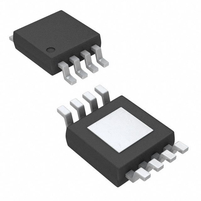
The RT8415 is available in the SOP-8 (Exposed Pad)
Applications
package.
Ordering Information
z
MR16 Lighting
z
Signage and Decorative LED Lighting
Architectural Lighting
High Power LED Lighting
Low Voltage Industrial Lighting
z
RT8415
Package Type
SP : SOP-8 (Exposed Pad-Option 2)
z
Lead Plating System
G : Green (Halogen Free and Pb Free)
z
z
Indicator and Emergency Lighting
Automotive LED Lighting
z
Note :
Pin Configuration
Richtek products are :
f
Thermal Shutdown Protection
SOP-8 (Exposed Pad) Package
z
(TOP VIEW)
RoHS compliant and compatible with the current
requirements of IPC/JEDEC J-STD-020.
f
8
GATE1
CS
2
OVP
3
VCOMP
4
Suitable for use in SnPb or Pb-free soldering processes.
GND
LX2
7
CREG
6
VCC
5
ISN
9
SOP-8 (Exposed Pad)
Simplified Application Circuit
D5
L1
D1
VCC
R1
OVP
D2
VL
AC 12V
ISN
Q1
D3
GATE1
CS
OVP
D4
CS
R4
July 2016
CREG
VCOMP
C1
Copyright © 2016 Richtek Technology Corporation. All rights reserved
COUT
C2
R2
VN
DS8415-00
RT8415
VCC
R3
BLD
RSENSE
ISN
LED+
D6
C5
LED-
C3
L2
LX2
GND
is a registered trademark of Richtek Technology Corporation.
www.richtek.com
1
�RT8415
Marking Information
RT8415
GSPYMDNN
RT8415GSP : Product Number
YMDNN : Date Code
Functional Pin Description
Pin No.
Pin Name
Pin Function
1
GATE1
The 1st stage output gate.
2
CS
The 1st stage current sense input.
3
OVP
Over-voltage protection sense input.
4
VCOMP
Compensation node. A compensation network between VCOMP and GND is
needed.
5
ISN
LED current sense amplifier negative input.
6
VCC
Power supply. For good bypass, place a ceramic capacitor near the VCC pin.
7
CREG
Internal regulator output. Place a 4.7PF Capacitor between CREG and GND
pins.
8
LX2
Switch node. The 2nd Stage Internal MOSFET Drain.
9 (Exposed Pad)
GND
Ground. The Exposed Pad must be soldered to a large PCB and connected to
GND for maximum power dissipation.
Copyright © 2016 Richtek Technology Corporation. All rights reserved
www.richtek.com
2
is a registered trademark of Richtek Technology Corporation.
DS8415-00
July 2016
�RT8415
Functional Block Diagram
ISN VCC
-110mV
V
Regulator
VCC
CREG
UV/OV
LX2
EN2
OVP
VCOMP
Core
Logic
EN2
EN1
Duty
Control
CREG
EN1
GATE1
GND
CS
Operation
The RT8415 VCC is supplied from the first stage Boost output.
The first stage is a constant output voltage Boost topology that controls the inductor current with excellent Power
Factor.
The second stage is a constant output current Buck topology. The current sense voltage threshold between the VCC
and ISN pins is only �110mV to minimize the power loss.
Copyright © 2016 Richtek Technology Corporation. All rights reserved
DS8415-00
July 2016
is a registered trademark of Richtek Technology Corporation.
www.richtek.com
3
�RT8415
Absolute Maximum Ratings (Note 1)
y Supply Voltage, VCC to GND -------------------------------------------------------------------------------------- ��0.3V to 40V
z
CREG, OVP, VCOMP, CS to GND -------------------------------------------------------------------------------- ��0.3V to 6V
z
LX2 to GND ------------------------------------------------------------------------------------------------------------- ��0.3V to 40V
z
VCC to ISN-------------------------------------------------------------------------------------------------------------- ��0.3V to 3V
z
Power Dissipation, PD @ TA = 25°C
z
SOP-8 (Exposed Pad) ---------------------------------------------------------------------------------------------- �2.46W
Package Thermal Resistance (Note 2)
SOP-8 (Exposed Pad), TJA ---------------------------------------------------------------------------------------- 40.6°C/W
SOP-8 (Exposed Pad), TJC ---------------------------------------------------------------------------------------- �2°C/W
z
Lead Temperature (Soldering, 10 sec.) ------------------------------------------------------------------------- �260qC
z
Junction Temperature ----------------------------------------------------------------------------------------------- �150qC
z
Storage Temperature Range -------------------------------------------------------------------------------------- ��65qC to 150qC
z
ESD Susceptibility (Note 3)
HBM (Human Body Model) ---------------------------------------------------------------------------------------- �2kV
MM (Machine Model) ----------------------------------------------------------------------------------------------- �200V
Recommended Operating Conditions (Note 4)
z
Supply Input Voltage, VCC ----------------------------------------------------------------------------------------- �4.5V to 36V
z
Ambient Temperature Range--------------------------------------------------------------------------------------- ��40qC to 85qC
z
Junction Temperature Range -------------------------------------------------------------------------------------- ��40qC to 125qC
Electrical Characteristics
(VCC = 20VDC, No Load, CLOAD = 1nF, TA = 25°C, unless otherwise specified.)
Parameter
Symbol
Test Conditions
Min
Typ
Max
Unit
Supply Voltage
CREG UVLO_ON
VUVLO_ON
OVP = 0V
--
4.2
--
V
CREG UVLO_OFF
VUVLO_OFF
OVP = 0V
--
3.9
--
V
VCC Shutdown Current
ISHDN
VCC = 2V
--
10
--
PA
VCC Quiescent Current
IQ
--
2
--
mA
VCC OVP Trigger Level
VCC_OVP
--
39
--
V
Internal Reference Voltage
VCREG
--
5
--
V
--
4.9
--
V
Supply Current
Internal Reference Voltage
(ICREG = �20mA)
ICREG = �20mA
Boost Converter
Stage 1 OVP
High Level
VOVP_H
--
1.88
--
V
Low Level
VOVP_L
1.52
1.6
1.68
V
--
1
--
PA
--
50
--
k:
OVP Pin Leakage Current
CS Input Impendence
IOVP
CS = �0.2V
Copyright © 2016 Richtek Technology Corporation. All rights reserved
www.richtek.com
4
is a registered trademark of Richtek Technology Corporation.
DS8415-00
July 2016
�RT8415
Parameter
Symbol
Test Conditions
Min
Typ
Max
Unit
UGATE1 Drive Sink
RUGATE1sk
Sink = 50mA
--
2
--
:
LGATE1 Drive Source
RLGATE1sr
Source = �50mA
--
1.5
--
:
GATE1 Default Pull Down
Resistor
RLGATE1sr
--
90
--
k:
103
110
117
mV
(dV1 + dV2) / 2
--
15
--
%
Sink = 100mA
--
0.2
--
:
Over-Temperature Threshold TSD
(Note 5)
--
150
--
o
Over-Temperature Threshold
'TSD
Hysteresis
(Note 5)
--
30
--
o
Buck Converter
ISN Threshold
VCC�VISN
Stage 2 Peak to Peak Sense
Voltage
LX2 Internal Switch RDS(ON)
RDS(ON)_LX2
Temperature Protection
C
C
Note 1. Stresses beyond those listed “Absolute Maximum Ratings” may cause permanent damage to the device. These are
stress ratings only, and functional operation of the device at these or any other conditions beyond those indicated in the
operational sections of the specifications is not implied. Exposure to absolute maximum rating conditions may affect
device reliability.
Note 2. TJA is measured under natural convection (still air) at TA = 25qC with the component mounted on a low
effective-thermal-conductivity two-layer test board on a JEDEC thermal measurement standard. TJC is measured at the
exposed pad of the package.
Note 3. Devices are ESD sensitive. Handling precaution recommended.
Note 4. The device is not guaranteed to function outside its operating conditions.
Note 5. Guaranteed by design.
Copyright © 2016 Richtek Technology Corporation. All rights reserved
DS8415-00
July 2016
is a registered trademark of Richtek Technology Corporation.
www.richtek.com
5
�RT8415
Typical Application Circuit
L1
D1
D5
R1
OVP
D2
LIN
RIN
VL
AC 12V
VCC
C6
RT8415
6
VCC
C2
R2
ISN
VN
CIN
D3
Q1
D4
CS R4
C1
COUT
5
7
1 GATE1
CREG
2 CS
3 OVP
8
LX2
4 VCOMP
R3
BLD
RSENSE
ISN
LED+
D6
C5
LED-
C3
L2
GND
9 (Exposed Pad)
Copyright © 2016 Richtek Technology Corporation. All rights reserved
www.richtek.com
6
is a registered trademark of Richtek Technology Corporation.
DS8415-00
July 2016
�RT8415
Typical Operating Characteristics
Quiescent Current vs. Temperature
2.6
2.4
2.4
Quiescent Current (mA)
Quiescent Current (mA)
Quiescent Current vs. VCC
2.6
2.2
2.0
1.8
1.6
1.4
2.2
2.0
1.8
1.6
1.4
OVP = 5V, VCC = 30V
OVP = 5V
1.2
1.2
0
5
10
15
20
25
30
35
-50
-25
0
25
50
75
100
125
Temperature (°C)
VCC (V)
�
�
VCC OVP vs. Temperature
CREG Voltage vs. VCC
42
7
6
CREG Voltage (V)
VCC OVP (V)
40
38
36
34
5
ICREG = 0mA
ICREG = �20mA
4
3
32
2
30
-50
-25
0
25
50
75
100
0
125
5
10
Temperature (°C)
15
20
25
30
35
VCC (V)
�
�
CREG Voltage vs. Temperature
ISN Sense Threshold vs. VCC
130
ISN Sense Threshold (mV)
5.4
CREG Voltage (V)
5.3
5.2
5.1
ICREG = 0mA
5.0
ICREG = �20mA
4.9
125
120
115
110
105
100
95
90
85
VCC = 30V
80
4.8
-50
-25
0
25
50
75
100
0
125
5
10
15
20
25
30
�
�
Copyright © 2016 Richtek Technology Corporation. All rights reserved
DS8415-00
July 2016
35
VCC (V)
Temperature (°C)
is a registered trademark of Richtek Technology Corporation.
www.richtek.com
7
�RT8415
LX2 RDS(ON) vs. VCC
0.30
130
0.25
LX2 RDS(ON) (Ω)
ISN Sense Threshold (mV)
ISN Sense Threshold vs. Temperature
140
120
110
100
90
0.20
0.15
0.10
0.05
VCC = 20V
80
0.00
-50
-25
0
25
50
75
100
125
Temperature (°C)
0
5
10
15
20
25
30
35
VCC (V)
�
�
�
LX2 RDS(ON) vs. Temperature
0.30
LX2 RDS(ON) (Ω)
0.25
0.20
0.15
0.10
0.05
VCC = 20V
0.00
-50
-25
0
25
50
75
100
125
Temperature (°C)
�
�
Copyright © 2016 Richtek Technology Corporation. All rights reserved
www.richtek.com
8
�
is a registered trademark of Richtek Technology Corporation.
DS8415-00
July 2016
�RT8415
Application Information
The RT8415 consists of a constant voltage Boost
controller and a constant output current Buck controller.
The Boost controller is based on a peak current, well
PFC control architecture, and designed to operate up
VCC Voltage Setting
to 1MHz to use a very small inductor for space
constrained applications.
1.88V, the power switch is turned off. The power switch
can be turned on again once the voltage at the OVP pin
Under-Voltage Lockout (UVLO)
drops below 1.6V. For Boost applications, the output
voltage can be set by the following equation :
The RT8415 includes an under-voltage lockout function
with 300mV hysteresis. The internal MOSFET turns off
when VCC falls below 3.9V (typ.).
VCC(MAX) = 1.88V u §¨1 + R1 ·¸
R2 ¹
©
CREG Regulator
R1 and R2 are the voltage divider resistors from VOUT
to GND with the divider center node connected to the
The CREG pin requires a capacitor for stable operation
and to store the charge for the large GATE switching
currents. Choose a 10V rated low ESR, X7R or X5R,
ceramic capacitor for best performance. A 4.7PF
capacitor will be adequate for many applications. Place
the capacitor close to the IC to minimize the trace
length to the CREG pin and to the IC ground. An
internal current limit on the CREG output protects the
RT8415 from excessive on-chip power dissipation. The
CREG pin has set the output to 4.2V (typ.) to protect
the internal FETs from excessive power dissipation
caused by not being fully enhanced. If the CREG pin is
used to drive extra circuits beside RT8415, the extra
loads should be limited to less than 10mA.
Average Output Current Setting
The output current that flows through the LED string is
set by an external resistor, RSENSE, which is connected
between the VCC and ISN terminal. The relationship
between output current, IOUT, and RSENSE is shown
below :
IOUT = 110mV
RSENSE
LED Current Ripple Reduction
Higher LED current ripple will shorten the LED life time
and increase heat accumulation of LED. To reduce the
LED current ripple, an output capacitor in parallel with
the LED should be added. The typical value of output
capacitor is 4.7PF.
The VCC voltage setting is equipped with an
over-voltage protection (OVP) function. When the
voltage at the OVP pin exceeds threshold approximately
OVP pin. For MR16 LED lamp application, the
minimum voltage of VCC should maintain above 25V for
stable operation.
The VCC voltage setting is equipped with an
Over-Voltage Protection function. When the voltage at
the VCC pin exceeds threshold approximately 39V, the
power switch is turned off.
Step-Down Converter Inductor Selection
The RT8415 implemented a simple high efficiency,
continuous mode inductive step-down converter. The
inductance L2 in Buck converter is determined by the
following factors : inductor ripple current, switching
frequency, VOUT/VCC ratio, internal MOSFET, topology
specifications, and component parameter. The
inductance L2 is calculated according to the following
equation :
L2 t ª¬ VCC(MAX) � VOUT � 0.11� �RDS(ON)_LX2 u IOUT � º¼
u
D2
f
� SW2 u 'IOUT �
where
f SW2 is the switching frequency of Buck controller (Hz).
RDS2(ON)_LX2 is the low-side switch on-resistance of
internal MOSFET M2. The typical value is 0.2:.
D2 is the duty cycle = VOUT / VCC.
IOUT is the required LED current (A).
'IOUT is the inductor peak-peak ripple current
(internally set to 0.3 x IOUT).
VCC is the Buck input voltage (V).
Copyright © 2016 Richtek Technology Corporation. All rights reserved
DS8415-00
July 2016
is a registered trademark of Richtek Technology Corporation.
www.richtek.com
9
�RT8415
VOUT is the total LED forward voltage (V).
L2 is the inductance (H).
The selected inductor must have saturation current
higher than the peak output LED current and
continuous current rating above the required average
output LED current. In general, the inductor saturation
current should be 1.5 times the LED current. In order to
minimize output current ripple, higher values of
inductance are recommended at higher supply
voltages. Because high values of inductance has high
line resistance, it will cause lower efficiency.
Step-Up Converter Inductor Selection
The RT8415 uses a continuous mode and well inductor
control to provide wide electronic transformer compatibility
step-up converter.
higher than the limit current of inductance L1. In
general, the inductor saturation current should be 1.2
times the limit current of inductance L1. A 10PH to
22PH inductor will meet the demand of most of the
RT8415 applications.
1st Stage Current Sense Resistor Selection
The resistor, R4, between CS and GND should be
selected to provide adequate switch current to drive the
application without exceeding the current limit
threshold set by the CS pin sense threshold of the
RT8415. The Sense resistor value can be calculated
according to the following equation :
R4 =
VCL
IL1_LIMIT
Where
Following the continuous mode mechanism, the
inductance L1 is calculated according to the following
equation :
IL1_LIMIT is the limit current of first inductor.
L1 t ª¬ VIN � VFBR � �RDS(ON)_Q1 u IL1 � � �R4 u IL1 � º¼
Diode Selection
u
D1
� fSW1 u 'IL1 �
The limit current of first inductor is calculated according
to the following equation :
VCL is the current limit threshold (0.125V, typ.).
To obtain better efficiency, the Schottky diode is
recommended for its low reverse leakage current, low
recovery time and low forward voltage. With its low
power dissipation, the Schottky diode outperforms
other silicon diodes and increases overall efficiency.
V
I L1_LIMIT = CL
R4
where
f SW1 is the switching frequency of Boost controller (Hz).
RDS(ON)_Q1 is the switch on-resistance of external
MOSFET Q1.
D1 is the duty cycle = (VCC � VIN ) / VCC.
IL1 is the input current. The typical value is 2A for MR16
application.
'IL1 is the inductor peak-peak ripple current (typically
set to 0.055 / R4).
VFBR is the bridge rectifier forward voltage (V).
VIN is the supply input voltage (V).
VCC is the Boost output voltage (V).
VCL is the current limit threshold (0.125V, typ.).
L1 is the inductance (H).
R4 is the CS resistance (:).
The selected inductor must have saturation current
Copyright © 2016 Richtek Technology Corporation. All rights reserved
www.richtek.com
10
Input Capacitor selection
Input capacitor has to supply peak current to the
inductor and flatten the current ripple on the input. The
low ESR condition is required to avoid increasing
power loss. The ceramic capacitor is recommended
due to its excellent high frequency characteristic and
low ESR, which is suitable for the RT8415. For
maximum stability over the entire operating
temperature range, capacitors with better dielectric are
suggested.
Thermal Protection
A thermal protection feature is to protect the RT8415
from excessive heat damage. When the junction
temperature exceeds 150qC, the thermal protection will
turn off the GATE1 and LX2 terminals. When the
junction temperature drops below 125qC, the RT8415
will turn on the GATE1 and LX2 terminals terminal and
return to normal operation.
is a registered trademark of Richtek Technology Corporation.
DS8415-00
July 2016
�RT8415
Thermal Considerations
Maximum Power Dissipation (W)1
3.0
The junction temperature should never exceed the
absolute maximum junction temperature TJ(MAX), listed
under Absolute Maximum Ratings, to avoid permanent
damage to the device. The maximum allowable power
dissipation depends on the thermal resistance of the IC
package, the PCB layout, the rate of surrounding airflow,
and the difference between the junction and ambient
temperatures. The maximum power dissipation can be
calculated using the following formula :
Two-Layer PCB
2.5
2.0
1.5
1.0
0.5
0.0
PD(MAX) = (TJ(MAX) �TA) / TJA
0
where TJ(MAX) is the maximum junction temperature, TA
is the ambient temperature, and TJA is the
25
50
75
100
125
Ambient Temperature (°C)
Figure 1. Derating Curve of Maximum Power
junction-to-ambient thermal resistance.
Dissipation
For continuous operation, the maximum operating
junction temperature indicated under Recommended
Operating Conditions is 125qC. The junction-to-ambient
thermal resistance,�TJA, is highly package dependent.
For a SOP-8 (Exposed Pad) package, the thermal
resistance, TJA, is 40.6qC/W on a standard JEDEC low
effective-thermal-conductivity two-layer test board. The
maximum power dissipation at TA = 25qC can be
calculated as below :
Layout Consideration
PCB layout is very important to design power switching
converter circuits. Some recommended layout
guidelines are suggested as follows :
f
The power components L1, D5, Q1, CIN, and COUT
must be placed as close to each other as possible to
reduce the ac current loop area. The power
PD(MAX) = (125qC ��25qC) / (40.6qC/W) = 2.46W for a
SOP-8 (Exposed Pad) package.
components L2, D6, and LX2 pin of device must be
The maximum power dissipation depends on the
operating ambient temperature for the fixed TJ(MAX) and
the ac current loop area. The PCB trace between
the thermal resistance, TJA. The derating curves in
Figure 1 allows the designer to see the effect of rising
power components must be as short and wide as
possible due to large current flow through these
ambient temperature
dissipation.
traces during operation.
on
the
maximum
placed as close to each other as possible to reduce
power
f
The capacitor COUT, C5 and external resistor,
RSENSE, must be placed as close as possible to the
VCC and ISN pins of the device respectively.
f
The GND should be connected to a strong ground
plane.
f
Keep the main current traces as short and wide as
possible.
Copyright © 2016 Richtek Technology Corporation. All rights reserved
DS8415-00
July 2016
is a registered trademark of Richtek Technology Corporation.
www.richtek.com
11
�RT8415
D5
L1
VIN
VCC
R1
COUT
OVP
R2
RSENSE
C6
ISN
LED+
D6
GND
VL
LIN
D1
D2
RIN
Q1
GATE1
CS
2
OVP
3
VCOMP
4
VN
D3
D4
CIN
R4
C5
L2
C1
GND
8
LX2
7
CREG
6
VCC
5
ISN
9
LED-
C2
C3
GND
CS
Figure 2. PCB Layout Guide
Copyright © 2016 Richtek Technology Corporation. All rights reserved
www.richtek.com
12
is a registered trademark of Richtek Technology Corporation.
DS8415-00
July 2016
�RT8415
Outline Dimension
Dimensions In Millimeters
Symbol
Dimensions In Inches
Min
Max
Min
Max
A
4.801
5.004
0.189
0.197
B
3.810
4.000
0.150
0.157
C
1.346
1.753
0.053
0.069
D
0.330
0.510
0.013
0.020
F
1.194
1.346
0.047
0.053
H
0.170
0.254
0.007
0.010
I
0.000
0.152
0.000
0.006
J
5.791
6.200
0.228
0.244
M
0.406
1.270
0.016
0.050
X
2.000
2.300
0.079
0.091
Y
2.000
2.300
0.079
0.091
X
2.100
2.500
0.083
0.098
Y
3.000
3.500
0.118
0.138
Option 1
Option 2
8-Lead SOP (Exposed Pad) Plastic Package
Richtek Technology Corporation
14F, No. 8, Tai Yuen 1st Street, Chupei City
Hsinchu, Taiwan, R.O.C.
Tel: (8863)5526789
Richtek products are sold by description only. Richtek reserves the right to change the circuitry and/or specifications without notice at any time. Customers should
obtain the latest relevant information and data sheets before placing orders and should verify that such information is current and complete. Richtek cannot assume
responsibility for use of any circuitry other than circuitry entirely embodied in a Richtek product. Information furnished by Richtek is believed to be accurate and
reliable. However, no responsibility is assumed by Richtek or its subsidiaries for its use; nor for any infringements of patents or other rights of third parties which may
result from its use. No license is granted by implication or otherwise under any patent or patent rights of Richtek or its subsidiaries.
Copyright © 2016 Richtek Technology Corporation. All rights reserved
DS8415-00
July 2016
is a registered trademark of Richtek Technology Corporation.
www.richtek.com
13
�


 工商网监
湘ICP备2023018690号
工商网监
湘ICP备2023018690号
