RT8453
Conceptual
High Voltage BUCK LED Driver
General Description
Features
The RT8453 is a Buck current mode PWM regulator for
High Voltage : VIN up to 40V
LED driving applications. It has a 1.5A switch on board
and can be operated with wide input range from 4.5V to
1.5A Switch Current
Current Mode PWM with 800kHz Switching
Frequency
40V. With a 800kHz operating frequency, the external
High efficiency is achieved with a 190mV current sensing.
Easy Dimming : Analog or Digital method
Programmable Soft Start to Avoid Inrush Current
Dimming can be either analog or PWM digital signal driven.
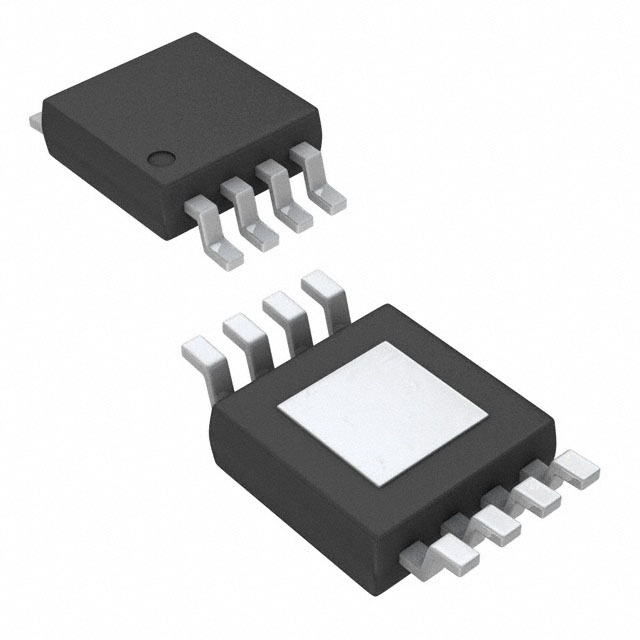
The RT8453 is available in SOP8 (Exposed pad) package.
VIN Under Voltage Lockout and Thermal Shutdown
RoHS Compliant and Halogen Free
PWMinductor and input/output capacitors can all be small.
Ordering Information
Applications
RT8453
GPS, Portable DVD Backlight
Package Type
SP : SOP-8 (Exposed Pad-Option 2)
Operating Temperature Range
G : Green (Halogen Free with Commercial Standard)
Note :
Desk Lights and Room Lighting
Industrial Display Backlight
Pin Configurations
(TOP VIEW)
Richtek Green products are :
RoHS compliant and compatible with the current require-
ISN
ments of IPC/JEDEC J-STD-020.
VC
2
ACTL
3
EN
4
Suitable for use in SnPb or Pb-free soldering processes.
8
GND
9
VCC
7
SW
6
GND
5
SS
SOP-8 (Exposed Pad)
Typical Application Circuit
V IN
4.5V to 40V
R2
190mV
C1
RT8453
8 VCC
Analog
Dimming
ISN 1
R3
3 ACTL
R4
C4
4 EN
5V
2
R1
10k
C2
3.3nF
VC
5 SS
C3
10nF
SW
GND
7
L
22uH
6, Exposed Pad (9)
Figure 1. Analog Dimming BUCK Configuration
DS8453-00C March 2009
www.richtek.com
1
�RT8453
Conceptual
VIN
4.5V to 40V
R2
190mV
C1
RT8453
8 VCC
ISN 1
R3
R4
3 ACTL
PWM
Dimming control
C4
4 EN
5V
2
R1
10k
C2
3.3nF
VC
5 SS
C3
10nF
SW
GND
7
L
22uH
6, Exposed Pad (9)
Figure 2. Digital Dimming BUCK Configuration Through ACTL Pin
Functional Pin Description
Pin No.
Pin Name
Pin Function
1
ISN
2
VC
Current Sense Amplifier Negative Input. Voltage threshold between V CC and ISN is
190mV.
PWM Converter Loop Compensation Node.
3
ACTL
Analog Dimming Control. Effective programming range is between 0.3V and 1.2V.
4
EN
Chip Enable (Active High). When low, chip is in shutdown mode.
5
SS
6,
GND
9 (Exposed Pad)
Soft Start. A capacitor of at least 10nF is required for soft start.
Ground. The exposed pad must be soldered to a large PCB and connected
to GND for maximum power dissipation.
7
SW
PWM Converter Switch Node.
8
VCC
Power Supply of the Chip. For good bypass, a low ESR capacitor is required.
www.richtek.com
2
DS8453-00C March 2009
�RT8453
Conceptual
Function Block Diagram
SW
OSC
S
-
VCC
R
+
4.5V
EN
+
1.4V
R
Shutdown
-
VC
GM
+
6uA
SS
ACTL
ISN
V CC
+
-
GND
V CC – V ISN
(mV)
190
0
0.3
1.2
VACTL (V)
Figure 3
DS8453-00C March 2009
www.richtek.com
3
�RT8453
Conceptual
Absolute Maximum Ratings
(Note 1)
Supply Input Voltage, VCC ----------------------------------------------------------------------------------------------- 45V
SW Pin Voltage at Switching Off, ISP, ISN -------------------------------------------------------------------------- 65V
ACTL ------------------------------------------------------------------------------------------------------------------------- 8V
EN, OVP Pin Voltage ---------------------------------------------------------------------------------------------------- 20V
Power Dissipation, PD @ TA = 25C
SOP-8 (Exposed Pad) --------------------------------------------------------------------------------------------------- 1.429W
Package Thermal Resistance (Note 4)
SOP-8 (Exposed Pad),
JA
--------------------------------------------------------------------------------------------- 75C/W
SOP-8 (Exposed Pad),
JC
--------------------------------------------------------------------------------------------- 28C/W
Junction Temperature ----------------------------------------------------------------------------------------------------- 150C
Lead Temperature (Soldering, 10 sec.) ------------------------------------------------------------------------------- 260C
Storage Temperature Range -------------------------------------------------------------------------------------------- n65C to 150C
ESD Susceptibility (Note 2)
HBM (Human Body Mode) ---------------------------------------------------------------------------------------------- 3kV
MM (Machine Mode) ------------------------------------------------------------------------------------------------------ 250V
Recommended Operating Conditions
(Note 3)
Junction Temperature Range -------------------------------------------------------------------------------------------- n40C to 125C
Ambient Temperature Range -------------------------------------------------------------------------------------------- n40C to 85C
Electrical Characteristics
(VCC = 12V, No Load, TA = 25C, unless otherwise specified)
Parameter
Symbol
Conditions
Min
Typ
Max
Unit
4.5
--
40
V
--
4
6
mA
--
250
--
A
--
1.4
--
V
--
--
0.5
A
170
190
210
mV
Overall
Supply Voltage
V CC
Supply Current
IVCC
VC
Shutdown Current
ISHDN
V EN
Shutdown Threshold
V EN
EN Input Current
0.4V (Switching off)
0.7V
V EN
5V
4.5V
common mode
Current Sense Amplifier
Input Threshold (VCC
VISN)
60V
Input Current
I ISN
V ISN = 24V
--
40
--
A
Output Current
IVC
2.4V > VC > 0.2V
--
20
--
A
--
0.7
--
--
--
3
A
--
0.2
--
V
600k
800k
1M
Hz
VC Threshold for PWM Switch Off
V
LED Dimming
Analog Dimming ACTL Pin Input Current IACTL
LED Current Off Threshold at ACTL
V ACTL
0.3V
VACTL
1.3V
PWM BOOST Converter
Switching Frequency
f SW
To be continued
www.richtek.com
4
DS8453-00C March 2009
�RT8453
Conceptual
Parameter
Maximum Duty Cycle
Symbol
Conditions
(Note 5)
SW On-Voltage
V SW
SW Current Limit
ILIM_SW
ISW = 0.5A
Min
Typ
Max
Unit
--
86
--
%
--
0.4
--
V
1.25
1.5
--
A
--
6
--
A
Soft Start
Soft Start SS Pin Current
ISS
VSS
2V
Note 1. Stresses beyond those listed under “Absolute Maximum Ratings ” may cause permanent damage to the device.
These are stress ratings only, and functional operation of the device at these or any other conditions beyond those
indicated in the operational sections of the specifications is not implied. Exposure to absolute maximum rating
conditions for extended periods may affect device reliability.
Note 2. Devices are ESD sensitive. Handling precaution is recommended.
Note 3. The device is not guaranteed to function outside its operating conditions.
Note 4.
JA
is measured in the natural convection at TA = 25C on a high effective four layers thermal conductivity test board of
JEDEC 51-7 thermal measurement standard.
Note 5. When the natural maximum duty cycle of 1MHz switching frequency is reached, the switching cycle will be skipped
(not reset) as the operating condition requires to effectively stretch and achieve higher on cycle than the natural
maximum duty cycle set by the 1MHz switching frequency.
DS8453-00C March 2009
www.richtek.com
5
�RT8453
Conceptual
Typical Operating Characteristics
(VCC-ISN) Threshold Voltage vs. Input Voltage
(VCC-ISN) Threshold Voltage vs. ACTL Voltage
200
190.0
180
187.5
160
185.0
140
182.5
120
180.0
100
80
177.5
60
175.0
40
172.5
VEN = 3V
170.0
4
7
20
VIN = 12V
0
0
10 13 16 19 22 25 28 31 34 37 40
0.25
0.5
0.75
1
1.25
1.5
ACTL Voltage (V)
Input Voltage (V)
Shutdown Current vs. Input Voltage
120
Efficiency vs. Input Voltage
100
90
100
80
70
80
60
50
60
40
40
30
20
20
VEN = 0V
0
4
7
10 13 16 19
22 25 28 31
10
ILOAD = 300mA
0
34 37 40
12
14
Input Voltage (V)
16
18
20
22
24
Input Voltage (V)
Switching Frequency vs. Temperature
880
Output Current vs. ACTL Voltage
700
870
600
860
500
850
840
400
830
300
820
810
200
800
100
790
VIN = 12V
780
-40 -25 -10
5
20
35
50
65
80
Temperature (C)
www.richtek.com
6
95 110 125
VIN = 12V, R2 = 0.3
0
0
0.25
0.5
0.75
1
1.25
1.5
ACTL Voltage (V)
DS8453-00C March 2009
�RT8453
Conceptual
ACTL Threshold Voltage vs. Input Voltage
Soft Start Current vs. Input Voltage
0.160
5.40
5.35
0.155
5.30
5.25
0.150
5.20
0.145
5.15
5.10
0.140
5.05
5.00
0.135
4.95
4.90
0.130
4
10
16
22
28
34
Input Voltage (V)
40
12
14
16
18
20
22
24
26
28
30
Input Voltage (V)
Power On from EN
3pcs LED Buck Application,
VIN = 12V, IOUT = 300mA
LED
(5V/Div)
VEN
(5V/Div)
IOUT
(200mA/Div)
Time (50s/Div)
DS8453-00C March 2009
www.richtek.com
7
�RT8453
Conceptual
A pplications Information
The RT8453 is specifically designed to be operated in
buck converter applications. This device uses a fixed
frequency, current mode control scheme to provide
excellent line and load regulation. The control loop has a
current sense amplifier to sense the voltage between the
VCC and ISN pins and provides an output voltage at the
VC pin. A PWM comparator then turns off the internal
power switch when the sensed power switch current
exceeds the compensated VC pin voltage. The power
switch will not reset by the oscillator clock in each cycle.
If the comparator does not turn off the switch in a cycle,
the power switch is on for more than a full switching period
until the comparator is tripped. In this manner, the
programmed voltage across the sense resistor is regulated
by the control loop.
The current through the sense resistor is set by the
programmed voltage and the sense resistance. The voltage
across the sense resistor can be programmed by the
analog or digital signal at the ACTL pin.
The protection schemes in RT8453 include overtemperature, and switch current-limit to prevent the
abnormal situation.
Frequency Compensation
The RT8453 has an external compensation pin (VC)
allowing the loop response optimized for specific
application. An external resistor in series with a capacitor
is connected from the VC pin to GND to provide a pole
and a zero for proper loop compensation. The typical value
for RT8453 is 10k and 3.3nF.
LED current Setting
The LED current can be calculated by the following
equation :
ILED(MAX)
VCC VISN
R2
Where,
VCC n VISN is the voltage between VCC and ISN (190mV
typ. if ACTL dimming is not applied) and the R2 is the
resister between VCC and ISN.
Current-Limit Protection
The RT8453 can limit the peak switch current by internal
over current protection feature. In normal operation, the
power switch is turned off when the switch current hits
the loop-set value. The over current protection function
will turn off the power switch independent of the loop control
when the peak switch current reaches around 1.5A.
Over Temperature Protection
The RT8453 has over temperature protection (OTP) function
to prevent the excessive power dissipation from
overheating. The OTP function will shut down switching
operation when the die junction temperature exceeds 150C
. The chip will automatically start to switch again when
the junction temperature cools off .
Inductor Selection
Choose an inductor that can handle the necessary peak
current without saturating, and ensure that the inductor
has a low DCR (copper-wire resistance) to minimize I2R
power losses. A 4.7H to 22H inductor will meet the
Soft Start
demand of most of the RT8453 applications.
The soft-start of RT8453 can be achieved by connecting a
Inductor manufacturers specify the maximum current rating
capacitor from SS pin to GND.
as the current where the inductance falls to certain
The built-in soft-start circuit reduces the start-up current
spike and output voltage overshoot. The soft-start time is
percentage of its nominal value typically 65%.
determined by the external capacitor charged by an internal
discontinuous and continuous modes occurs, the value of
6uA constant charging current. The SS pin directly limits
the required output inductor (L), can be approximated by
the rate of voltage rise on the VC pin, which in turn limits
the following equation :
In Buck application where the transition between
the peak switch current.
The value of the soft-start capacitor is user-defined to
satisfy the designer's request.
www.richtek.com
8
L
f
VOUT
IL(MAX)
1
VOUT
VIN(MAX)
DS8453-00C March 2009
�RT8453
Conceptual
The ripple current IL could be calculated :
IL
VOUT
f L
1
temperature, TA is the ambient temperature and the
JA is
the junction to ambient thermal resistance.
VOUT
VIN
For recommended operating conditions specification of
Where,
RT8453, The maximum junction temperature is 125C.
VOUT = output voltage.
The junction to ambient thermal resistance
is layout
dependent. For SOP-8 (exposed pad) packages, the
VIN = input voltage.
thermal resistance
JA
is 75°C/W on the standard JEDEC
51-7 four layers thermal test board. The maximum power
f = switching frequency.
Schottky Diode Selection
The Schottky diode, with their low forward voltage drop
JA
dissipation at TA = 25C can be calculated by following
formula :
and fast switching speed, is necessary for RT8453
applications. In addition, power dissipation, reverse voltage
PD(MAX) = (125C n 25C) / (75C/W) = 1.333W for
rating and pulsating peak current are the important
parameters of the Schottky diode must be considered.
The maximum power dissipation depends on operating
ambient temperature for fixed T J(MAX) and thermal
The diode's average current rating must exceed the average
resistance
output current. The diode conducts current only when the
power switch is turned off (typically less than 50% duty
derating curves allows the designer to see the effect of
rising ambient temperature on the maximum power
cycle).
dissipation allowed.
SOP-8 (exposed pad)
Capacitor Selection
1.6
The input capacitor reduces current spikes from the input
supply and minimizes noise injection to the converter. For
1.4
most RT8453 applications, a 4.7F ceramic capacitor is
sufficient. A value higher or lower may be used depending
on the noise level from the input supply and the input current
0.4
ESR
1
8 f COUT
Thermal Considerations
For continuous operation, do not exceed absolute
maximum operation junction temperature. The maximum
power dissipation depends on the thermal resistance of
IC package, PCB layout, the rate of surroundings airflow
SOP-8 (Exposed Pad)
0.8
In Buck Application, the output capacitor is typically a
ceramic capacitor and is selected based on the output
IL
Four Layers PCB
1.0
0.6
VOUT
For RT8453 packages, the Figure 3 of
1.2
to the converter.
voltage ripple requirements. The output ripple, VOUT, is
determined by the following equation :
JA.
0.2
0.0
0
25
50
75
100
125
Ambient Temperature (°C)
Figure 3. Derating Curves for RT8453 Package
Layout Guideline
PCB layout is very important to design power switching
converter circuits. Some recommended layout guide lines
are suggested as follows:
and temperature difference between junction to ambient.
The power components L1, D1 and C1 must be placed
The maximum power dissipation can be calculated by
as close to each other as possible to reduce the ac
following formula :
current loop area. The PCB trace between power
components must be as short and wide as possible
PD(MAX) = ( TJ(MAX) n TA ) /
JA
Where T J(MAX) is the maximum operation junction
DS8453-00C March 2009
due to large current flow through these traces during
operation.
www.richtek.com
9
�RT8453
Conceptual
Place L1 and D1 connected to SW pin as close as
possible. The trace should be as short and wide as
possible.
The input capacitors C1 must be placed as close to
VCC pin as possible.
Place the compensation components to VC pin as close
as possible to avoid noise pick up.
R2
C4
C1
ISN
VC
R1
C2
ACTL
EN
8
2
3
4
GND
9
Locate the compensation
components to VC pin as
close as possible.
VCC
7
SW
6
GND
5
SS
D1
L1
Place these components
as close as possible.
Locate input capacitor as
close VCC as possible.
C3
Figure 4
www.richtek.com
10
DS8453-00C March 2009
�RT8453
Conceptual
Datasheet Revision History
Version
00C
Data
2009/3/18
DS8453-00C March 2009
Page No.
Item
Description
first edition
www.richtek.com
11
�RT8453
Conceptual
Outline Dimension
H
A
M
EXPOSED THERMAL PAD
(Bottom of Package)
Y
J
X
B
F
C
I
D
Dimensions In Millimeters
Symbol
Dimensions In Inches
Min
Max
Min
Max
A
4.801
5.004
0.189
0.197
B
3.810
4.000
0.150
0.157
C
1.346
1.753
0.053
0.069
D
0.330
0.510
0.013
0.020
F
1.194
1.346
0.047
0.053
H
0.170
0.254
0.007
0.010
I
0.000
0.152
0.000
0.006
J
5.791
6.200
0.228
0.244
M
0.406
1.270
0.016
0.050
X
2.000
2.300
0.079
0.091
Y
2.000
2.300
0.079
0.091
X
2.100
2.500
0.083
0.098
Y
3.000
3.500
0.118
0.138
Option 1
Option 2
8-Lead SOP (Exposed Pad) Plastic Package
Richtek Technology Corporation
Richtek Technology Corporation
Headquarter
Taipei Office (Marketing)
5F, No. 20, Taiyuen Street, Chupei City
Hsinchu, Taiwan, R.O.C.
8F, No. 137, Lane 235, Paochiao Road, Hsintien City
Taipei County, Taiwan, R.O.C.
Tel: (8863)5526789 Fax: (8863)5526611
Tel: (8862)89191466 Fax: (8862)89191465
Email: marketing@richtek.com
Information that is provided by Richtek Technology Corporation is believed to be accurate and reliable. Richtek reserves the right to make any change in circuit design,
specification or other related things if necessary without notice at any time. No third party intellectual property infringement of the applications should be guaranteed
by users when integrating Richtek products into any application. No legal responsibility for any said applications is assumed by Richtek.
www.richtek.com
12
DS8453-00C March 2009
�


 工商网监
湘ICP备2023018690号
工商网监
湘ICP备2023018690号