®
RT8477A
High Voltage High Current LED Driver
General Description
Features
The RT8477A is a current mode PWM controller designed
to drive an external MOSFET for high current LED
applications with wide input voltage (4.5V to 50V) and
output voltage (up to 50V) ranges. With internal 380kHz
operating frequency, the size of the external PWM inductor
and input/output capacitors can be minimized. High
efficiency is achieved by a 100mV current sensing control.
LED Dimming control can be done by analog.
Buck Constant Current Converter
High Voltage : VIN up to 50V, VOUT up to 50V
380kHz Fixed Switching Frequency
Analog or PWM Control Signal for LED Dimming
Internal Soft-Start to Avoid Inrush Current
Under-Voltage Lockout
Thermal Shutdown
Applications
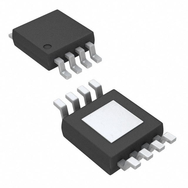
The RT8477A is now available in the SOP-8 (Exposed
Pad) package.
Desk Lights and Room Lighting
Industrial Display Backlight
Ordering Information
Pin Configurations
RT8477A
Package Type
SP : SOP-8 (Exposed Pad-Option 1)
(TOP VIEW)
8
VCC
Lead Plating System
G : Green (Halogen Free and Pb Free)
Note :
ISP
2
ISN
3
VC
4
GND
CREG
7
DRV
6
SENS
5
CTL
9
Richtek products are :
SOP-8 (Exposed Pad)
RoHS compliant and compatible with the current requirements of IPC/JEDEC J-STD-020.
Marking Information
Suitable for use in SnPb or Pb-free soldering processes.
RT8477AGSP : Product Number
RT8477A
GSPYMDNN
YMDNN : Date Code
Simplified Application Circuit
D1
R1
VIN
C1
R5
C4
RT8477A
...
VCC
LEDs
ISP
C6
L1
ISN
CTL
Analog Dimming
CREG
C2
GND
Copyright © 2014 Richtek Technology Corporation. All rights reserved.
DS8477A-01
December 2014
M1
DRV
SENS
R3
R4
VC
C3
R2
C5
is a registered trademark of Richtek Technology Corporation.
www.richtek.com
1
�RT8477A
Functional Pin Description
Pin No.
Pin Name
Pin Function
1
VCC
Supply Voltage Input. For good bypass, a low ESR capacitor is required.
2
ISP
Positive Input Current Sense.
3
ISN
Negative Input Current Sense. Voltage threshold between ISP and ISN is 100mV.
4
VC
VC Compensation Node for Current Loop.
5
CTL
Analog Dimming Control Input. Effective programming range is 0.33V to 2V.
6
SENS
Current Sense Input for LED Current. Connect the current sense resistor
between external N-MOSFET switch and the ground.
7
DRV
External MOSFET Switch Gate Driver Output.
8
CREG
Regulator Output. Placed 1F capacitor to stabilize the 5V regulator output.
GND
Ground. The exposed pad must be soldered to a large PCB and connected to
GND for maximum power dissipation.
9 (Exposed Pad)
Function Block Diagram
S
OSC
-
VCC
4.5V
CREG
R
+
DRV
R
5V
LDO
+
-
VC
SENS
Soft-Start
GM
+
CTL
ISN
ISP
+
-
GND
Copyright © 2014 Richtek Technology Corporation. All rights reserved.
www.richtek.com
2
is a registered trademark of Richtek Technology Corporation.
DS8477A-01
December 2014
�RT8477A
Operation
The RT8477A is a current mode PWM controller designed
to drive an external MOSFET for high current LED
applications. This device uses a fixed frequency, currentmode control scheme to provide excellent line and load
regulation.
The control loop has a current sense amplifier which
senses the voltage between the ISP and ISN pins.
A PWM comparator then turns off the external power
switch when the sensed power switch current exceeds
the internal compensated voltage. The power switch will
not be reset by the oscillator clock in each cycle. If the
comparator does not turn off the switch in a cycle, the
power switch will be on for more than a full switching period
until the comparator is tripped. In this manner, the
programmed voltage across the sense resistor is regulated
by the control loop.
The current through the sense resistor is set by the
programmed voltage and the sense resistance. The voltage
across the sense resistor can be programmed by the
analog or digital signal at the CTL pin with good dimming
linearity. The max sense threshold of 100mV can be
obtained with CTL pin voltage greater than 2V (max
dimming point). The sense threshold is intentionally forced
to zero by an internal comparator when the CTL pin voltage
is less than around 0.33V (min dimming point). Because
of that, the actual sense threshold right before cut off may
vary from part to part over process variation.
The RT8477A provides protection functions which include
over-temperature, and switch current limit to prevent
abnormal situations.
Copyright © 2014 Richtek Technology Corporation. All rights reserved.
DS8477A-01
December 2014
is a registered trademark of Richtek Technology Corporation.
www.richtek.com
3
�RT8477A
Absolute Maximum Ratings
(Note 1)
Supply Input Voltage, VCC ------------------------------------------------------------------------------------ −0.3V to 60V
ISP, ISN ------------------------------------------------------------------------------------------------------------ −0.3V to 60V
SENS, DRV, CREG, VC Pin Voltage ----------------------------------------------------------------------- −0.3V to 5.5V
CTL Pin Voltage ------------------------------------------------------------------------------------------------- −0.3V to 20V (Note 2)
Power Dissipation, PD @ TA = 25°C
SOP-8 (Exposed Pad) ----------------------------------------------------------------------------------------- 3.26W
Package Thermal Resistance (Note 3)
SOP-8 (Exposed Pad), θJA ------------------------------------------------------------------------------------ 30.6°C/W
SOP-8 (Exposed Pad), θJC ----------------------------------------------------------------------------------- 3.4°C/W
Junction Temperature ------------------------------------------------------------------------------------------- 150°C
Lead Temperature (Soldering, 10 sec.) --------------------------------------------------------------------- 260°C
Storage Temperature Range ---------------------------------------------------------------------------------- −65°C to 150°C
ESD Susceptibility (Note 4)
HBM (Human Body Model) ------------------------------------------------------------------------------------ 2kV
Recommended Operating Conditions
(Note 5)
Supply Input Voltage, VCC ------------------------------------------------------------------------------------ 4.5V to 50V
Junction Temperature Range ---------------------------------------------------------------------------------- −40°C to 125°C
Ambient Temperature Range ---------------------------------------------------------------------------------- −40°C to 85°C
Electrical Characteristics
(VCC = 12V, TA = 25°C, unless otherwise specified)
Parameter
Symbol
Test Conditions
Min
Typ
Max
Unit
4.5
5
5.5
V
mA
Overall
Regulator Output Voltage
VCREG
ICREG = 20mA
Supply Current
IVCC
VCTL = 3V
--
--
3
VIN Under Voltage Lockout
Threshold
VUVLO
VIN Rising
--
4.25
4.5
VIN Falling
--
4.2
--
4.5 Common Mode 20V
95
100
105
IISP
VISP = 24V
--
150
--
IISN
VISN = 24V
--
50
--
IVC
2.4V > VC > 0.3V
--
10
--
A
--
0.4
--
V
--
1
2
A
V
Current Sense Amplifier
Input Threshold (VISP VISN)
Input Current
Output Current
VC Threshold for CTL Switch Off
mV
A
LED Dimming
0.2V VCTL 1.2V
Input Current of CTL Pin
ICTL
LED Current Off Threshold at CTL
VCTL_OFF
--
0.33
0.4
V
LED Current On Threshold at CTL
VCTL_ON
--
2
2.5
V
Copyright © 2014 Richtek Technology Corporation. All rights reserved.
www.richtek.com
4
is a registered trademark of Richtek Technology Corporation.
DS8477A-01
December 2014
�RT8477A
Parameter
Symbol
Test Conditions
Min
Typ
Max
Unit
330
380
430
kHz
--
--
100
%
--
200
--
ns
4.5
5
5.5
V
Gate Driver Source
1
2.5
--
A
Gate Driver Sink
1
3.5
--
A
--
2
--
ms
100
150
--
mV
PWM Converter
Switch Frequency
f SW
Maximum Duty Cycle
DMAX
(Note 6)
Minimum On-Time
Gate High Voltage
VGATE_H
Soft-Start Time
Sense Current Limit Threshold
IGATE = 20mA
(Note 7)
ISENS_LIM
Over-Temperature Protection
Thermal Shutdown Temperature
TSD
--
150
--
C
Thermal Shutdown Hysteresis
T SD
--
20
--
C
Note 1. Stresses beyond those listed “Absolute Maximum Ratings” may cause permanent damage to the device. These are
stress ratings only, and functional operation of the device at these or any other conditions beyond those indicated in
the operational sections of the specifications is not implied. Exposure to absolute maximum rating conditions may
affect device reliability.
Note 2. If connected with a 20kΩ serial resistor, CTL can go up to 40V.
Note 3. θJA is measured at TA = 25°C on a high effective thermal conductivity four-layer test board per JEDEC 51-7. θJC is
measured at the exposed pad of the package.
Note 4. Devices are ESD sensitive. Handling precaution is recommended.
Note 5. The device is not guaranteed to function outside its operating conditions.
Note 6. When the natural maximum duty cycle of the switching frequency is reached, the switching cycle will be skipped (not
reset) as the operating condition requires to effectively stretch and achieve higher on cycle than the natural maximum
duty cycle set by the switching frequency.
Note 7. Guaranteed by design, not subjected to production test.
Copyright © 2014 Richtek Technology Corporation. All rights reserved.
DS8477A-01
December 2014
is a registered trademark of Richtek Technology Corporation.
www.richtek.com
5
�RT8477A
Typical Application Circuit
D1
R1
VIN
4.5V to 50V
C1
10µF
0.1
RT8477A
1
C6
1µF
Analog Dimming
VCC
LEDs
ISP 2
L1
22µH
ISN 3
5 CTL
8
CREG
C2
1µF 9
GND
DRV
7
SENS 6
4
VC
C4
1µF
...
R5
10
M1
R3 51
R4 10k
C3
1nF
R2
0.03
C5
3.3nF
Figure 1. Buck Configuration
Copyright © 2014 Richtek Technology Corporation. All rights reserved.
www.richtek.com
6
is a registered trademark of Richtek Technology Corporation.
DS8477A-01
December 2014
�RT8477A
Typical Operating Characteristics
Efficiency vs. Input Voltage
Supply Current vs. VCC
100
1.5
VOUT
VOUT
VOUT
VOUT
Efficiency (%)
96
94
=
=
=
=
21V
18V
15V
12V
Supply Current (mA)
Buck, LED Current = 2A, L = 22μH
98
92
VOUT = 9V
90
88
86
VOUT = 6V
84
1.4
1.3
1.2
1.1
82
80
1.0
5
15
25
35
45
55
0
5
10
15
25
30
35
40
45
50
VCC (V)
Input Voltage (V)
ISP - ISN Threshold vs. Temperature
LED Current vs. VCTL
120
450
LED Current = 300mA, LED = 6pcs
ISP - ISN Threshold (mV)
400
350
LED Current (mA)
20
300
250
200
150
100
110
100
90
80
50
VCC = 24V
70
0
0.3
0.6
0.9
1.2
1.5
1.8
2.1
2.4
2.7
-40
3
-10
20
50
80
VCTL (V)
Temperature (°C)
Frequency vs. VCC
Power On from VIN
110
140
410
Frequency (kHz)1
400
VIN
(20V/Div)
390
VOUT
(10V/Div)
380
370
IOUT
(2A/Div)
VIN = 30V, IOUT = 2A, LED = 42pcs, L = 47μH
360
0
5
10
15
20
25
30
35
40
45
50
Time (2.5ms/Div)
VCC (V)
Copyright © 2014 Richtek Technology Corporation. All rights reserved.
DS8477A-01
December 2014
is a registered trademark of Richtek Technology Corporation.
www.richtek.com
7
�RT8477A
Power Off from VIN
VIN
(20V/Div)
VOUT
(10V/Div)
IOUT
(2A/Div)
VIN = 30V, IOUT = 2A, LED = 42pcs, L = 47μH
Time (25ms/Div)
Copyright © 2014 Richtek Technology Corporation. All rights reserved.
www.richtek.com
8
is a registered trademark of Richtek Technology Corporation.
DS8477A-01
December 2014
�RT8477A
Application Information
The RT8477A is a current mode PWM controller designed
to drive an external MOSFET for high current LED
applications. This device uses a fixed frequency, current
mode control scheme to provide excellent line and load
regulation. The control loop has a current sense amplifier
which senses the voltage between the ISP and ISN pins.
The power switch will not be reset by the oscillator clock
in each cycle. If the comparator does not turn off the
switch in a cycle, the power switch will be on for more
than a full switching period until the comparator is tripped.
In this manner, the programmed voltage across the sense
resistor is regulated by the control loop.
Frequency Compensation
The RT8477A has an external compensation pin, allowing
the loop response to be optimized for specific applications.
An external resistor in series with a capacitor is connected
from the VC pin to GND to provide a pole and a zero for
proper loop compensation. The typical value for the
RT8477A is 10k and 3.3nF.
LED Current Setting
The LED current can be calculated by the following
equation :
V(ISP ISN)
ILED(MAX) =
R1
where V(ISP − ISN) is the voltage between ISP and ISN
(100mV typ. if CTL dimming is not applied) and the R1 is
the resister between ISP and ISN.
Sense Resistor Selection
The resistor, R2, between the Source of the external NMOSFET and GND should be selected to provide adequate
switch current to drive the application without exceeding
the current limit threshold set by the SENSE pin sense
threshold of RT8477A. The Sense resistor value can be
calculated according to the formula below :
R2
Current Limlit Threshold Minimum Value
IOCP
where IOCP is about 1.33 to 1.5 times of inductor peak
current IPEAK.
The placement of R2 should be close to the source of the
N-MOSFET and the IC GND of the RT8477A. The SENSE
Copyright © 2014 Richtek Technology Corporation. All rights reserved.
DS8477A-01
December 2014
pin input to RT8477 should be a Kelvin sense connection
to the positive terminal of R2.
Over-Temperature Protection
The RT8477A has Over-Temperature Protection (OTP)
function to prevent the excessive power dissipation from
overheating. The OTP function will shut down switching
operation when the die junction temperature exceeds
150°C. The chip will automatically start to switch again
when the die junction temperature cools off.
Inductor Selection
The converter operates in discontinuous conduction mode
when the inductance value is less than the value LBCM.
With an inductance greater than LBCM, the converter
operates in Continuous Conduction Mode (CCM). The
inductance LBCM is determined by the following equations.
For Buck application :
LBCM
VOUT
VIN VOUT
2 IOUT f
VIN
where
VOUT = output voltage.
VIN = input voltage.
f = operating frequency.
IOUT = LED current.
Choose an inductance based on the operating frequency,
input voltage and output voltage to provide a current mode
ramp signal during the MOSFET on period for PWM control
loop regulation. The inductance also determines the
inductor ripple current. Operating the converter in CCM is
recommended, which will have the smaller inductor ripple
current and hence the less conduction losses from all
converter components.
As a design example, to design the peak to peak inductor
ripple to be ±30% of the output current, the following
equations can be used to estimate the size of the needed
inductance :
For Buck application :
L=
VOUT
VIN VOUT
2 0.3 IOUT f
VIN
is a registered trademark of Richtek Technology Corporation.
www.richtek.com
9
�RT8477A
The inductor must also be selected with a saturation
current rating greater than the maximum inductor current
during normal operation. The maximum inductor current
can be calculated by the following equations.
For Buck application :
IPEAK = IOUT +
VOUT VIN VOUT
2 L f
VIN
where
η is the efficiency of the power converter.
Schottky Diode Selection
Thermal Considerations
For continuous operation, do not exceed absolute
maximum junction temperature. The maximum power
dissipation depends on the thermal resistance of the IC
package, PCB layout, rate of surrounding airflow, and
difference between junction and ambient temperature. The
maximum power dissipation can be calculated by the
following formula :
PD(MAX) = (TJ(MAX) − TA) / θJA
where TJ(MAX) is the maximum junction temperature, TA is
the ambient temperature, and θJA is the junction to ambient
thermal resistance.
The Schottky diode, with their low forward voltage drop
and fast switching speed, is necessary for RT8477A
applications. In addition, power dissipation, reverse voltage
rating and pulsating peak current are important parameters
of the Schottky diode that must be considered. The diode's
average current rating must exceed the average output
current. The diode conducts current only when the power
switch is turned off (typically less than 50% duty cycle).
For recommended operating condition specifications, the
maximum junction temperature is 125°C. The junction to
ambient thermal resistance, θJA, is layout dependent. For
SOP-8 (Exposed Pad) package, the thermal resistance,
θJA, is 30.6°C/W on a standard JEDEC 51-7 four-layer
Capacitor Selection
PD(MAX) = (125°C − 25°C) / (30.6°C/W) = 3.26W for
SOP-8 (Exposed Pad) package
VOUT
1
IL ESR +
8 f COUT
The maximum power dissipation depends on the operating
ambient temperature for fixed T J(MAX) and thermal
resistance, θJA. The derating curve in Figure 2 allows the
designer to see the effect of rising ambient temperature
on the maximum power dissipation.
3.6
Maximum Power Dissipation (W)1
The input capacitor reduces current spikes from the input
supply and minimizes noise injection to the converter. For
most RT8477A applications, a 4.7μF ceramic capacitor is
sufficient. A value higher or lower may be used depending
on the noise level from the input supply and the input
current to the converter. In Buck application, the output
capacitor is typically ceramic and selection is mainly
based on the output voltage ripple requirements. The
output ripple, ΔVOUT, is determined by the following
equation :
thermal test board. The maximum power dissipation at TA
= 25°C can be calculated by the following formula :
Four-Layer PCB
3.2
2.8
2.4
2.0
1.6
1.2
0.8
0.4
0.0
0
25
50
75
100
125
Ambient Temperature (°C)
Figure 2. Derating Curve of Maximum Power Dissipation
Copyright © 2014 Richtek Technology Corporation. All rights reserved.
www.richtek.com
10
is a registered trademark of Richtek Technology Corporation.
DS8477A-01
December 2014
�RT8477A
Layout Considerations
PCB layout is very important when designing power
switching converter circuits. Some recommended layout
guide lines are as follows :
The power components M1, L1, D1 and C4 must be
placed as close to each other as possible to reduce the
ac current loop area. The PCB trace between power
components must be as short and wide as possible
due to large current flow through these traces during
operation.
Place M1, L1 and D1 as close to each other as possible.
The trace should be as short and wide as possible.
The input capacitor C6 must be placed as close to VCC
pin as possible.
VIN power trace to ISP
must be wide and short.
Keep the ISP and ISN with
The Kelvin sense connection.
ISP
VIN
R1
C1
ISN
D1
...
Locate input capacitor as
close VCC as possible.
R5
L1
C2
VCC
C6
R4
ISP
2
ISN
3
VC
4
GND
8
CREG
7
DRV
6
SENS
5
CTL
9
Power trace must be wide
and short when compared
to the normal trace.
M1
R3
C3
C5
C4
Place these components as
close as possible.
R2
GND
Locate the compensation Components
to VC pin as Close as possible.
Normal trace.
Figure 3. PCB Layout Guide
Copyright © 2014 Richtek Technology Corporation. All rights reserved.
DS8477A-01
December 2014
is a registered trademark of Richtek Technology Corporation.
www.richtek.com
11
�RT8477A
Outline Dimension
H
A
M
EXPOSED THERMAL PAD
(Bottom of Package)
Y
J
X
B
F
C
I
D
Dimensions In Millimeters
Symbol
Dimensions In Inches
Min
Max
Min
Max
A
4.801
5.004
0.189
0.197
B
3.810
4.000
0.150
0.157
C
1.346
1.753
0.053
0.069
D
0.330
0.510
0.013
0.020
F
1.194
1.346
0.047
0.053
H
0.170
0.254
0.007
0.010
I
0.000
0.152
0.000
0.006
J
5.791
6.200
0.228
0.244
M
0.406
1.270
0.016
0.050
X
2.000
2.300
0.079
0.091
Y
2.000
2.300
0.079
0.091
X
2.100
2.500
0.083
0.098
Y
3.000
3.500
0.118
0.138
Option 1
Option 2
8-Lead SOP (Exposed Pad) Plastic Package
Richtek Technology Corporation
14F, No. 8, Tai Yuen 1st Street, Chupei City
Hsinchu, Taiwan, R.O.C.
Tel: (8863)5526789
Richtek products are sold by description only. Richtek reserves the right to change the circuitry and/or specifications without notice at any time. Customers should
obtain the latest relevant information and data sheets before placing orders and should verify that such information is current and complete. Richtek cannot
assume responsibility for use of any circuitry other than circuitry entirely embodied in a Richtek product. Information furnished by Richtek is believed to be
accurate and reliable. However, no responsibility is assumed by Richtek or its subsidiaries for its use; nor for any infringements of patents or other rights of third
parties which may result from its use. No license is granted by implication or otherwise under any patent or patent rights of Richtek or its subsidiaries.
www.richtek.com
12
DS8477A-01
December 2014
�


 工商网监
湘ICP备2023018690号
工商网监
湘ICP备2023018690号
