®
RT9073A
1μ
μA IQ, 250mA Low-Dropout Linear Regulator
General Description
Features
The RT9073A is a low-dropout (LDO) voltage regulators
with enable function that operates from 1.2V to 5.5V. It
provides up to 250mA of output current and offers lowpower operation in miniaturized packaging.
The features of low quiescent current as low as 1μA and
almost zero disable current is ideal for powering the battery
equipment to a longer service life. The RT9073A is stable
with the ceramic output capacitor over its wide input range
from 1.2V to 5.5V and the entire range of output load
current (0mA to 250mA).
Ordering Information
RT9073APackage Type
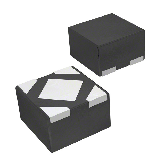
QZ : ZQFN-4L 1x1 (Z-Type)
(ZDFN-4L 1x1)
Y : SC-82
Lead Plating System
G : Green (Halogen Free and Pb Free)
Output Voltage
09 : 0.9V
1K : 1.05V
12 : 1.2V
15 : 1.5V
18 : 1.8V
19 : 1.9V
1μ
μA Ground Current at no Load
PSRR = 75dB at 1kHz
±2% Output Accuracy
250mA (VIN ≥ 2.3V) Output Current with EN
Low (0.1μ
μA) Disable Current
1.2V to 5.5V Operating Input Voltage
Dropout Voltage : 0.5V at 250mA when VOUT ≥ 3V
Support Fixed Output Voltage 0.9V, 1.05V, 1.2V, 1.5V,
1.8V, 1.9V, 2.5V, 2.7V, 2.8V, 2.9V, 3V, 3.3V
Stable with Ceramic or Tantalum Capacitor
Current Limit Protection
Over Temperature Protection
ZQFN-4L 1x1 (ZDFN-4L 1x1), SC-82 Packages
Available
Applications
Portable, Battery Powered Equipment
Ultra Low Power Microcontrollers
Notebook computers
Marking Information
For marking information, contact our sales representative
directly or through a Richtek distributor located in your
area.
25 : 2.5V
27 : 2.7V
28 : 2.8V
29 : 2.9V
30 : 3.0V
33 : 3.3V
Special Request: Any Voltage
Between 0.9V and 3.3V under
specific business agreement
Note :
Richtek products are :
RoHS compliant and compatible with the current require-
Suitable for use in SnPb or Pb-free soldering processes.
ments of IPC/JEDEC J-STD-020.
Copyright © 2015 Richtek Technology Corporation. All rights reserved.
DS9073A-00 April 2015
is a registered trademark of Richtek Technology Corporation.
www.richtek.com
1
�RT9073A
Pin Configurations
(TOP VIEW)
VOUT
4
1
VIN
SGND
GND
2
5
3
VIN
VOUT
4
3
2
EN
EN
ZQFN-4L 1x1 (ZDFN-4L 1x1)
GND
SC-82 (SSOT-24)
Functional Pin Description
Pin No.
ZQFN-4L 1x1 (ZDFN-4L 1x1) SC-82 (SSOT-24)
Pin Name
Pin Function
1
3
VOUT
Output of the Regulator.
2
2
GND
Ground.
3
1
EN
Enable Control Input.
4
4
VIN
Supply Voltage Input.
5 (Exposed Pad)
--
SGND
Substrate of Chip. Leave floating or tie to GND.
Copyright © 2015 Richtek Technology Corporation. All rights reserved.
www.richtek.com
2
is a registered trademark of Richtek Technology Corporation.
DS9073A-00 April 2015
�RT9073A
Function Block Diagram
VIN
VOUT
Current/Thermal
Sense
GND
R1
Bandgap
Reference
+
-
EN
R2
Operation
Basic operation
Current Limit Protection
The RT9073A is a low quiescent current linear regulator
designed especially for low external components system.
The input voltage range is from 1.2V to 5.5V.
The RT9073A provides current limit function to prevent
the device from damages during over-load or shorted-circuit
condition. This current is detected by an internal sensing
transistor.
Output Transistor
The RT9073A builds in a P-MOSFET output transistor
which provides a low switch-on resistance for low dropout
voltage applications.
Error Amplifier
The Error Amplifier compares the internal reference voltage
with the output feedback voltage from the internal divider,
and controls the Gate voltage of P-MOSFET to support
good line regulation and load regulation at output voltage.
Over Temperature Protection
The over temperature protection function will turn off the
P-MOSFET when the junction temperature exceeds 150°C
(typ.), VIN ≥ 1.5V and the output current exceeds 30mA.
Once the junction temperature cools down by
approximately 20°C, the regulator will automatically
resume operation.
Enable
The RT9073A delivers the output power when it is set to
enable state. When it works in disable state, there is no
output power and the operation quiescent current is almost
zero.
Copyright © 2015 Richtek Technology Corporation. All rights reserved.
DS9073A-00 April 2015
is a registered trademark of Richtek Technology Corporation.
www.richtek.com
3
�RT9073A
Absolute Maximum Ratings
(Note 1)
VIN, VOUT, EN to GND --------------------------------------------------------------------------------------------------- −0.3V to 6.5V
VOUT to VIN ---------------------------------------------------------------------------------------------------------------- −6.5V to 0.3V
Power Dissipation, PD @ TA = 25°C
ZQFN-4L 1x1 (ZDFN-4L 1x1) -------------------------------------------------------------------------------------------- 1.07W
SC-82 ------------------------------------------------------------------------------------------------------------------------ 0.28W
Package Thermal Resistance (Note 2)
ZQFN-4L 1x1 (ZDFN-4L 1x1), θJA -------------------------------------------------------------------------------------- 92.7°C/W
ZQFN-4L 1x1 (ZDFN-4L 1x1), θJC ------------------------------------------------------------------------------------- 62.3°C/W
SC-82, θJA ------------------------------------------------------------------------------------------------------------------- 345.6°C/W
Lead Temperature (Soldering, 10 sec.) ------------------------------------------------------------------------------- 260°C
Junction Temperature ----------------------------------------------------------------------------------------------------- 150°C
Storage Temperature Range -------------------------------------------------------------------------------------------- −65°C to 150°C
ESD Susceptibility (Note 3)
HBM (Human Body Model) ---------------------------------------------------------------------------------------------- 2kV
MM (Machine Model) ------------------------------------------------------------------------------------------------------ 200V
Recommended Operating Conditions
(Note 4)
Input Voltage, VIN --------------------------------------------------------------------------------------------------------- 1.2V to 5.5V
Junction Temperature Range -------------------------------------------------------------------------------------------- −40°C to 125°C
Ambient Temperature Range -------------------------------------------------------------------------------------------- −40°C to 85°C
Electrical Characteristics
(VOUT + 1 < VIN < 5.5V, TA = 25°C, unless otherwise specified)
Parameter
Output Voltage Range
Symbol
Dropout Voltage (ILOAD =
250mA) (Note 5)
VCC Consumption Current
VDROP
VDROP
IQ
Copyright © 2015 Richtek Technology Corporation. All rights reserved.
www.richtek.com
4
Min
Typ
Max
Unit
0.9
--
3.3
V
ILOAD = 1mA
2
--
2
%
0.9V VOUT 1.2V
--
0.5
0.65
1.2V VOUT 1.5V
--
0.3
0.4
1.5V VOUT 1.8V
--
0.2
0.24
1.8V VOUT 2.5V
--
0.15
0.18
2.5V VOUT 3V
--
0.1
0.15
3V VOUT
--
0.08
0.12
0.9V VOUT 1.2V
--
1.25
1.45
1.2V VOUT 1.5V
--
1
1.2
1.5V VOUT 1.8V
--
0.81
0.9
1.8V VOUT 2.5V
--
0.68
0.8
2.5V VOUT 3V
--
0.51
0.6
3V VOUT
--
0.45
0.6
ILOAD = 0mA, VOUT ≦ 5.5V
--
1
3
VOUT
DC Output Accuracy
Dropout Voltage (ILOAD = 50mA)
(Note 5)
Test Conditions
V
V
A
is a registered trademark of Richtek Technology Corporation.
DS9073A-00 April 2015
�RT9073A
Parameter
Symbol
Test Conditions
Min
Typ
Max
Unit
Shutdown GND Current
VEN = 0V
--
0.1
0.5
A
Shutdown Leakage
Current
VEN = 0V, VOUT = 0V
--
0.1
0.5
A
VEN = 5.5V
--
--
0.1
A
1.2V VIN 1.5V
--
--
0.6
1.5V VIN 1.8V
--
--
0.3
1.8V VIN 2.1V
--
--
0.1
2.1V VIN 5.5V
--
--
0.15
EN Input Current
IEN
LINE
Line Regulation
ILOAD = 10mA
%
Load Regulation
LOAD
1mA < ILOAD < 200mA
--
--
1
%
Power Supply Rejection
Ratio
PSRR
VIN = 3V, ILOAD = 50mA,
COUT = 1F, VOUT = 2.5V, f = 1kHz
--
75
--
dB
VOUT = 0.9V
--
39
--
VOUT = 1.2V
--
46
--
VOUT = 1.8V
--
48
--
VOUT = 3.3V
--
58
--
Peak output current
260
350
500
mA
VOUT = 0.5 x VOUT(normal)
190
270
350
mA
COUT = 1F,
ILOAD = 30mA,
BW = 10Hz to
100kHz,
VIN = VOUT + 2V
Output Voltage Noise
Output Current Limit
ILIM
Fold-Back Current Limit
VRMS
Logic-High
VIH
VIN = 5V
1.2
--
--
Logic-Low
VIL
VIN = 5V
--
--
0.4
Thermal Shutdown
Temperature
TSD
ILOAD = 30mA, VIN 1.5V
--
150
--
C
Thermal Shutdown
Hysteresis
TSD
--
20
--
C
Enable Input
Voltage
V
Note 1. Stresses beyond those listed “Absolute Maximum Ratings” may cause permanent damage to the device. These are
stress ratings only, and functional operation of the device at these or any other conditions beyond those indicated in
the operational sections of the specifications is not implied. Exposure to absolute maximum rating conditions may
affect device reliability.
Note 2. θJA is measured at TA = 25°C on a high effective thermal conductivity four-layer test board per JEDEC 51-7. θJC is
measured at the exposed pad of the package.
Note 3. Devices are ESD sensitive. Handling precaution is recommended.
Note 4. The device is not guaranteed to function outside its operating conditions.
Note 5. The dropout voltage is defined as VIN − VOUT, when VOUT is 98% of the normal value of VOUT.
Copyright © 2015 Richtek Technology Corporation. All rights reserved.
DS9073A-00 April 2015
is a registered trademark of Richtek Technology Corporation.
www.richtek.com
5
�RT9073A
Typical Application Circuit
RT9073A
VIN
EN
4
CIN
1µF
3
VIN
VOUT
1
COUT
1µF
VOUT
EN
GND
2
Copyright © 2015 Richtek Technology Corporation. All rights reserved.
www.richtek.com
6
is a registered trademark of Richtek Technology Corporation.
DS9073A-00 April 2015
�RT9073A
Typical Operating Characteristics
Output Voltage vs. Temperature
Output Voltage vs. Temperature
0.91
3.32
0.90
Output Voltage (V)
Output Voltage (V)
3.31
3.30
3.29
ILOAD = 1mA
ILOAD = 250mA
3.28
3.27
ILOAD = 1mA
ILOAD = 250mA
0.89
0.88
0.87
3.26
VIN = 5V, VOUT = 3.3V
VIN = 5V, VOUT = 0.9V
0.86
3.25
-50
-25
0
25
50
75
100
-50
125
-25
0
25
50
75
100
125
Temperature (°C)
Temperature (°C)
Output Voltage vs. Input Voltage
Output Voltage vs. Output Current
3.33
0.904
0.902
Output Voltage (V)
Outout Voltage (V)
3.32
0.900
0.898
0.896
0.894
3.31
3.3
3.29
0.892
VOUT = 0.9V, ILOAD = 1mA
VIN = 5V, VOUT = 3.3V
3.28
0.890
1
1.5
2
2.5
3
3.5
4
4.5
5
0
5.5
30
90
120
150
180
210
240
Ground Current vs. Temperature
Ground Current vs. Input Voltage
2.1
1.5
1.8
1.4
Ground Current (μA)
Ground Current (μA)
60
Output Current (mA)
Input Voltage (V)
1.5
1.2
0.9
0.6
1.3
1.2
1.1
1
0.9
0.3
VIN = 5V, VOUT = 3.3V
VOUT = 0.9V
0.8
0
1
1.5
2
2.5
3
3.5
4
4.5
5
Input Voltage (V)
Copyright © 2015 Richtek Technology Corporation. All rights reserved.
DS9073A-00 April 2015
5.5
-50
-25
0
25
50
75
100
125
Temperature (°C)
is a registered trademark of Richtek Technology Corporation.
www.richtek.com
7
�RT9073A
Shutdown Current vs. Temperature
Shutdown Current vs. Input Voltage
0.50
VOUT = 0.9V, VEN = 0V
Shutdown Current (μA)1
0.45
Shutdown Current (μA)1
0.30
0.40
0.35
0.30
0.25
0.20
0.15
0.10
VEN = 0V
0.25
0.20
0.15
0.10
VIN = 5V
VIN = 3.5V
0.05
0.05
0.00
0.00
1.2 1.6
2
2.4 2.8 3.2 3.6
4
-50
4.4 4.8 5.2 5.6
-25
0
Input Voltage (V)
EN Threshold vs. Input Voltage
0.70
25
50
75
100
125
Temperature (°C)
EN Threshold vs. Temperature
1.00
EN_H
0.60
0.80
EN_L
EN Threshold (V)
EN Threshold (V)
0.65
0.55
0.50
0.45
0.40
EN_H
0.60
EN_L
0.40
0.20
0.35
VIN = 5V
0.00
0.30
1.2 1.6
2
2.4 2.8 3.2 3.6
4
-50
4.4 4.8 5.2 5.6
-25
0
Dropout Voltage vs. Temperature
0.40
50
75
100
125
Dropout Voltage vs. Output Current
1.6
VIN = 3.3V
0.35
VOUT = 0.9V
1.4
0.30
0.25
Dropout Voltage (V)
Dropout Voltage (V)
25
Temperature (°C)
Input Voltage (V)
ILOAD = 100mA
0.20
0.15
ILOAD = 50mA
0.10
ILOAD = 20mA
0.05
1.2
1.0
TA = 125°C
TA = 85°C
TA = 25°C
TA = −40°C
0.8
0.6
0.4
0.2
0.00
0.0
-50
-25
0
25
50
75
100
Temperature (°C)
Copyright © 2015 Richtek Technology Corporation. All rights reserved.
www.richtek.com
8
125
0
50
100
150
200
250
Output Current (mA)
is a registered trademark of Richtek Technology Corporation.
DS9073A-00 April 2015
�RT9073A
Dropout Voltage vs. Output Current
1.4
Dropout Voltage vs. Output Current
1.2
VOUT = 1.5V
1.0
Dropout Voltage (V)
Dropout Voltage (V)
1.2
VOUT = 2.5V
1.0
0.8
0.6
TA = 125°C
TA = 85°C
TA = 25°C
TA = −40°C
0.4
0.2
0.8
TA = 125°C
TA = 85°C
TA = 25°C
TA = −40°C
0.6
0.4
0.2
0.0
0.0
0
50
100
150
200
0
250
50
Output Current (mA)
Fold-Back Current Limit (mA)
VIN = 5V
Current Limit (mA)
480
VOUT = 0.9V
380
VOUT = 3.3V
330
-50
GND Current (μA)
250
VIN = 5V
370
VOUT = 0.9V
320
VOUT = 3.3V
270
220
280
200
200
Fold-Back Current Limit vs. Temperature
420
430
150
Output Current (mA)
Current Limit vs. Temperature
530
100
-25
0
25
50
75
100
125
-50
-25
0
25
50
75
Temperature (°C)
Temperature (°C)
Ground Current vs. Load Current
Power On from EN
100
125
VIN = 5V
150
VIN
(2V/Div)
VEN
(2V/Div)
VOUT
(2V/Div)
100
TA = −40°C
TA = 25°C
TA = 125°C
50
I LOAD
(100mA/Div)
0
0.01
0.1
1
10
100
1000
10000
VIN = 5V
Time (50μs/Div)
Load Current (mA)
Copyright © 2015 Richtek Technology Corporation. All rights reserved.
DS9073A-00 April 2015
is a registered trademark of Richtek Technology Corporation.
www.richtek.com
9
�RT9073A
Power Off from EN
Line Transient
VIN
(2V/Div)
VEN
(2V/Div)
VOUT
(2V/Div)
VIN
(2V/Div)
VOUT
(5mV/Div)
I LOAD
(100mA/Div)
VIN = 5V
VIN = 2.4V to 5.5V, VOUT = 0.9V, ILOAD = 10mA
Time (25μs/Div)
Time (250μs/Div)
Load Transient
PSRR vs. Frequency
0
VIN
(200mV/Div)
VIN = 3.5V, ILOAD = 150mA
VIN = 3V, ILOAD = 50mA
VIN = 3.5V, ILOAD = 50mA
PSRR (dB)
-20
-40
-60
-80
I LOAD
(100mA/Div)
VIN = 5V, VOUT = 3.3V, ILOAD = 10mA to 250mA
VOUT = 2.5V, COUT = 2.2μF
-100
Time (250μs/Div)
10
100
1000
10000
100000
1000000
Frequency (Hz)
Output
Noise
Output Noise
VIN = 2.9V, VOUT = 0.9V, ILOAD = 100mA
COUT = 1μF, f = 10Hz to 100kHz
Noise(μV)
Noise(μV)
Output
Output Noise
Noise
300
270
240
210
180
150
120
90
60
30
0
-30
-60
-90
-120
-150
-180
-210
-240
-270
-300
0
1
2
3
4
5
6
7
8
sec (m)
Copyright © 2015 Richtek Technology Corporation. All rights reserved.
www.richtek.com
10
9
10
300
270
240
210
180
150
120
90
60
30
0
-30
-60
-90
-120
-150
-180
-210
-240
-270
-300
VIN = 5.3V, VOUT = 3.3V, ILOAD = 100mA
COUT = 1μF, f = 10Hz to 100kHz
0
1
2
3
4
5
6
7
8
9
10
sec (m)
is a registered trademark of Richtek Technology Corporation.
DS9073A-00 April 2015
�RT9073A
Application Information
Like any low dropout linear regulator, the RT9073A’s
external input and output capacitors must be properly
selected for stability and performance. Use a 1μF or larger
input capacitor and place it close to the IC's VIN and GND
pins. Any output capacitor meeting the minimum 1mΩ
ESR (Equivalent Series Resistance) requirement may be
used. Place the output capacitor close to the IC's VOUT
and GND pins. Increasing capacitance and decreasing ESR
can improve the circuit's PSRR and line transient response.
Enable
The RT9073A has an EN pin to turn on or turn off the
regulator, When the EN pin is in logic high, the regulator
will be turned on. The shutdown current is almost 0μA
typical. The EN pin may be directly tied to VIN to keep the
part on. The Enable input is CMOS logic and cannot be
left floating.
resistance, θJA, is layout dependent. For ZQFN-4L 1x1
(ZDFN-4L 1x1) package, the thermal resistance, θJA, is
92.7°C/W on a standard JEDEC 51-7 four-layer thermal
test board. For SC-82 (SSOT-24) package, the thermal
resistance, θJA, is 345.6°C/W on a standard JEDEC 51-7
four-layer thermal test board. The maximum power
dissipation at TA = 25°C can be calculated by the following
formula :
PD(MAX) = (125°C − 25°C) / (92.7°C/W) = 1.07W for
ZQFN-4L 1x1 (ZDFN-4L 1x1) package
PD(MAX) = (125°C − 25°C) / (345.6°C/W) = 0.28W for
SC-82 (SSOT-24) package
The maximum power dissipation depends on the operating
ambient temperature for fixed T J(MAX) and thermal
resistance, θJA. The derating curve in Figure 1 allows the
designer to see the effect of rising ambient temperature
on the maximum power dissipation.
Current Limit
Thermal Considerations
For continuous operation, do not exceed absolute
maximum junction temperature. The maximum power
dissipation depends on the thermal resistance of the IC
package, PCB layout, rate of surrounding airflow, and
difference between junction and ambient temperature. The
maximum power dissipation can be calculated by the
following formula :
1.6
Maximum Power Dissipation (W)1
The RT9073A contains an independent current limiter,
which monitors and controls the pass transistor's gate
voltage, limiting the output current to 0.35A (typ.). The
current limiting level is reduced to around 250mA named
fold-back current limit when the output voltage is further
decreased. The output can be shorted to ground indefinitely
without damaging the part.
Four-Layer PCB
1.2
ZQFN-4L 1x1 (ZDFN-4L 1x1)
0.8
0.4
SC-82 (SSOT-24)
0.0
0
25
50
75
100
125
Ambient Temperature (°C)
Figure 1. Derating Curve of Maximum Power Dissipation
PD(MAX) = (TJ(MAX) − TA) / θJA
where TJ(MAX) is the maximum junction temperature, TA is
the ambient temperature, and θJA is the junction to ambient
thermal resistance.
For recommended operating condition specifications the
maximum junction temperature is 125°C and TA is the
ambient temperature. The junction to ambient thermal
Copyright © 2015 Richtek Technology Corporation. All rights reserved.
DS9073A-00 April 2015
is a registered trademark of Richtek Technology Corporation.
www.richtek.com
11
�RT9073A
Outline Dimension
1
1
2
2
DETAIL A
Pin #1 ID and Tie Bar Mark Options
Note : The configuration of the Pin #1 identifier is optional,
but must be located within the zone indicated.
Symbol
Dimensions In Millimeters
Dimensions In Inches
Min.
Max.
Min.
Max.
A
0.300
0.400
0.012
0.016
A1
0.000
0.050
0.000
0.002
A3
0.117
0.162
0.005
0.006
b
0.175
0.275
0.007
0.011
D
0.900
1.100
0.035
0.043
D2
0.450
0.550
0.018
0.022
E
0.900
1.100
0.035
0.043
E2
0.450
0.550
0.018
0.022
e
L
0.625
0.200
0.025
0.300
0.008
0.012
H
0.039
0.002
H1
0.064
0.003
Z-Type 4L QFN 1x1 Package
Copyright © 2015 Richtek Technology Corporation. All rights reserved.
www.richtek.com
12
is a registered trademark of Richtek Technology Corporation.
DS9073A-00 April 2015
�RT9073A
D
e
H
L
B
C
b1
b
A
A1
e
Symbol
Dimensions In Millimeters
Dimensions In Inches
Min
Max
Min
Max
A
0.800
1.100
0.031
0.043
A1
0.000
0.100
0.000
0.004
B
1.150
1.350
0.045
0.053
b
0.150
0.400
0.006
0.016
b1
0.350
0.500
0.014
0.020
C
1.800
2.450
0.071
0.096
D
1.800
2.200
0.071
0.087
e
1.300
0.051
H
0.080
0.260
0.003
0.010
L
0.200
0.460
0.008
0.018
SC-82 Surface Mount Package
Richtek Technology Corporation
14F, No. 8, Tai Yuen 1st Street, Chupei City
Hsinchu, Taiwan, R.O.C.
Tel: (8863)5526789
Richtek products are sold by description only. Richtek reserves the right to change the circuitry and/or specifications without notice at any time. Customers should
obtain the latest relevant information and data sheets before placing orders and should verify that such information is current and complete. Richtek cannot
assume responsibility for use of any circuitry other than circuitry entirely embodied in a Richtek product. Information furnished by Richtek is believed to be
accurate and reliable. However, no responsibility is assumed by Richtek or its subsidiaries for its use; nor for any infringements of patents or other rights of third
parties which may result from its use. No license is granted by implication or otherwise under any patent or patent rights of Richtek or its subsidiaries.
DS9073A-00 April 2015
www.richtek.com
13
�