RT9114B
Dual Channel Digital Audio System with EQ and Frequency
DRC Control
General Description
Features
The RT9114B is a high efficiency, I2S-input, stereo
channel audio power amplifier delivering 2x20W into 8
BTL speaker loads. It can deliver over 90% power
efficiency and eliminate the need for heat-sink.
The built-in anti-pop functions can reduce the speaker’s
pop noise under all kind of scenarios. Built-in protection
circuits can provide over-temperature, over-current,
over-voltage, and under-voltage protections and report
error status.
The RT9114B is an I2S device receiving all clocks from
external sources. It can support both master and slave
mode with wide input sampling rate from 8kHz to 96kHz.
A fully programmable data path routes these channels
to the internal speaker drivers.
Equalization
Programmable Coefficients for DRC Filters and
Supporting Multi-Compression Ratios
Built-In DC Blocking Filters
Protection Features : UVLO, OVP, OCP, OTP and
DCP
Filter-Less Application
VQFN-28L Thermally-Enhanced Package
RoHS Compliant and Halogen Free
The RT9114B features three band DRC and flexible
multi-band biquads for anti-clipping, power limiting, and
speaker equalization.
Wide Input Supply Range : 8V to 26.4V
2x20W at into 8 BTL at 20V
2x9W at into 8 BTL at 12V
Support Stereo Channels Output
Sampling Frequency from 8kHz to 96kHz
Built-In Anti-Pop Function for BTL BD
Modulations
> 24 Programmable Biquads for Speaker
Applications
LCD-TV
Monitors
Home Audio
Amusement Equipment
Electronic Music Equipment
Simplified Application Circuit
3.3V
8V to 26.4V
DVDD PVDDL/PVDDR
Digital
Audio
Interface
BSTPL
MCLK
SCLK
LRCK
VOUTPL
SDI
SDO
VOUTNL
LC
Filter
BSTNL
RT9114B
2
I C
Control
SDA
SCL
BSTPR
VOUTTPR
Control
Inputs
PWDNN
RESETB
VOUTTNR
FAULTB
BSTNR
LC
Filter
A_SEL
Copyright © 2021 Richtek Technology Corporation. All rights reserved.
DS9114B-03
November 2021
is a registered trademark of Richtek Technology Corporation.
www.richtek.com
1
�RT9114B
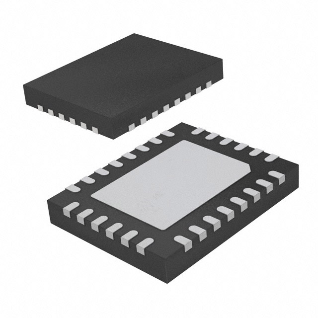
Pin Configuration
Ordering Information
(TOP VIEW)
RT9114B
SCL
SDA
A_SEL
FAULTB
PWDNN
BSTPL
Package Type
QV : VQFN-28L 4x5 (V-Type)
Lead Plating System
G : Green (Halogen Free and Pb Free)
28 27 26 25 24 23
SDI
SDO
RESETB
LRCK
SCLK
MCLK
DVSS
VR_DIG
Note :
Richtek products are :
RoHS compliant and compatible with the current
requirements of IPC/JEDEC J-STD-020.
Suitable for use in SnPb or Pb-free soldering processes.
1
22
2
21
3
20
4
PVSS
5
6
19
18
17
7
29
8
16
15
VOUTPL
PVDDL
VOUTNL
BSTNL
BSTNR
VOUTNR
PVDDR
VOUTPR
9 10 11 12 13 14
0E=YM
DNN
DVDD
AVSS
AVCC
GVDD
VR_ANA
BSTPR
Marking Information
0E= : Product Code
YMDNN : Date Code
VQFN-28L 4x5
Functional Pin Description
Pin No.
Pin Name
IO
Pin Function
2
1
SDI
DI
I S data input.
2
SDO
DO
I2S data output.
3
RESETB
DI
Reset, low active.
4
LRCK
DI
I2S L/R clock input.
5
SCLK
DI
I2S bit clock input.
6
MCLK
DI
Master clock input.
7
DVSS
P
Ground for digital circuits.
8
VR_DIG
P
1.8V digital supply voltage generated by internal LDO.
9
DVDD
P
3.3V power supply for I/O and HP.
10
AVSS
P
Ground for analog circuits.
11
AVCC
P
26.4V power supply for analog circuits.
12
GVDD
P
Internal power supply generated by LDO.
13
VR_ANA
P
Analog reference voltage.
14
BSTPR
P
Bootstrap supply for VOUTPR.
15
VOUTPR
16
PVDDR
17
VOUTNR
18
BSTNR
AO
P
AO
P
Positive output of RCH.
26.4V power supply for RCH.
Negative output of RCH.
Bootstrap supply of VOUTNR.
Copyright © 2021 Richtek Technology Corporation. All rights reserved.
www.richtek.com
2
is a registered trademark of Richtek Technology Corporation.
DS9114B-03
November 2021
�RT9114B
Pin No.
Pin Name
IO
19
BSTNL
20
VOUTNL
21
PVDDL
22
VOUTPL
23
BSTPL
P
Bootstrap supply for VOUTPL.
24
PWDNN
DI
Power down pin, low active.
25
FAULTB
DO
Fault indicator (low active).
26
A_SEL
DI
Slave address selection
27
SDA
DIO
28
SCL
DI
I2C clock input.
P
Ground.
29
PVSS
(Exposed Pad)
P
Pin Function
AO
P
AO
Bootstrap supply of VOUTNL.
Negative output of LCH.
26.4V power supply for LCH.
Positive output of LCH.
I2C data input/output.
Copyright © 2021 Richtek Technology Corporation. All rights reserved.
DS9114B-03
November 2021
is a registered trademark of Richtek Technology Corporation.
www.richtek.com
3
�RT9114B
Functional Block Diagram
SCL
Reg
Control
2
I C
SDA
LRCK
SCLK
Audio
Interface
SDI
DSP Function
(Mixer/DC-Block Filter/EQ/Gain/DRC)
Digital
Filter
SRC
DAC
SDO
Power
Stage
De-pop
control
Clock
Management
PLL
Detection
Power
Sequence
Control
OC/OT/
OV/UV/DC
Protection
PWDNN
MCLK
Speaker
Operation
Error Reporting
pin turns-ON/OFF.
The FAULTB pin is error report output pin. Any fault
will pull FAULTB to low. This pin is open-drain
Over-Current Protection
configuration, need pull-up resistor.
device from damages during overload or short-circuit
conditions. The current are detected by an internal
sensing circuit. Once overload happens, the OCP
function is designed to operate the latch mode.
Clock Detection
The RT9114B can accept SCLK to be as 32fs, 48fs
and 64fs and support only a 1xfs LRCK. The internal
oscillator will check MCLK or SCLK input constantly. If
clock is lost, the RT9114B will mute and shutdown the
power stage automatically.
Volume Control
The RT9114B have master volume MS_VOL and
each channel volume CH1_VOL, CH2_VOL control.
The step of each volume is 0.0625dB per step, from
24dB to mute. CH1 and CH2 also have each mute
control, CH1_MUTE and CH2_MUTE.
Built-In Anti-POP Function
An internal soft-start function controls the Duty rampup rate of the output PWM voltage to minimize the
POP noise during start-up. Similarly, when power
shut-down, the duty also ramp-down to eliminate the
POP noise. This function also acts when the PWDNN
Copyright © 2021 Richtek Technology Corporation. All rights reserved.
www.richtek.com
4
The RT9114B provides OCP function to prevent the
Under-Voltage Protection
The RT9114B monitors the voltage on PVDD voltage
threshold. When the voltage on PVDDL/R pin falls
below the under-voltage threshold, 6.5V (typ.), the
UVP circuit turns off the output immediately. Or the
latch mode can be configured to use.
Over-Voltage Protection
The RT9114B monitors the voltage on PVDD voltage
threshold. When the voltage on PVDDL/R pin rise
behind the over-voltage threshold, 30V, the OVP
circuit turns off the output immediately and operates in
cycle by cycle auto-recovery mode. Or the latch mode
can be configured to use.
Over-Temperature Protection
The over-temperature protection function will turn off
is a registered trademark of Richtek Technology Corporation.
DS9114B-03
November 2021
�RT9114B
the power MOSFET when the junction temperature
exceeds 150°C. Once the junction temperature cools
down by approximately 30°C, the regulator will
automatically resume operation. Or the latch mode
can be configured to use.
Copyright © 2021 Richtek Technology Corporation. All rights reserved.
DS9114B-03
November 2021
is a registered trademark of Richtek Technology Corporation.
www.richtek.com
5
�RT9114B
Absolute Maximum Ratings
(Note 1)
Supply Voltage, AVCC, PVDDL, PVDDR ------------------------------------------------------------- 0.3V to 32V
Supply Voltage, DVDD ------------------------------------------------------------------------------------- 0.3V to 3.6V
Speaker Amplifier Output Voltage, VOUTXX --------------------------------------------------------- 0.3V to 32V
BSTXX to PVSS DC ---------------------------------------------------------------------------------------- 0.3V to 37V
SCL, SDA ----------------------------------------------------------------------------------------------------- 0.3V to 6V
LRCK, SCLK, SDI, MCLK, PWDNN, A_SEL, RESETB-------------------------------------------- 0.3V to DVDD + 0.3V
GND to PVSS ------------------------------------------------------------------------------------------------ 0.3V to 0.3V
VOUTPR, VOUTNR, VOUTPL, VOUTNL ------------------------------------------------------------- 10V to 37V
Power Dissipation, PD @ TA = 25C
(Note 5)
VQFN-28L 4x5 ----------------------------------------------------------------------------------------------- 4.56W
Package Thermal Resistance
(Note 2)
VQFN-28L 4x5, JA ----------------------------------------------------------------------------------------- 27.4C/W
VQFN-28L 4x5, JC ----------------------------------------------------------------------------------------- 1.7C/W
Lead Temperature (Soldering, 10sec.) ----------------------------------------------------------------- 260C
Junction Temperature -------------------------------------------------------------------------------------- 150C
Storage Temperature Range ----------------------------------------------------------------------------- 65C to 150C
ESD Susceptibility
(Note 3)
HBM (Human Body Model) ------------------------------------------------------------------------------- 2kV
Recommended Operating Conditions
(Note 4)
Supply Input Voltage, DVDD ----------------------------------------------------------------------------- 3.0V to 3.6V
Supply Input Voltage, PVDDL, PVDDR, AVCC ------------------------------------------------------ 8V to 26.4V
Supply Input Voltage, PVDDL, PVDDR ---------------------------------------------------------------- 8V to 26.4V
Ambient Temperature Range----------------------------------------------------------------------------- 40C to 85C
Junction Temperature Range ---------------------------------------------------------------------------- 40C to 150C
Electrical Characteristics
(PVDD = 12V, DVDD = 3.3V, RL = 8, TA = 25C, unless otherwise specified)
Parameter
VIH : High-LevelPWDNN, Input Voltage
A_SEL
VIL : Low-LevelInput Voltage
FAULTB
VOL : Low-LevelOutput Voltage
DVDD Quiescent Current
(Normal Mode)
Symbol
Min
Typ
Max
DVDD
x0.7
--
--
--
--
DVDD
x0.3
IPULLUP = 3mA
--
--
0.4
PWDNN = 3.3V, 0dBFS input, for
DVDD, no load, no LC filter
--
10
15
PWDNN = 3.3V, switch 50% duty
for DVDD, no load, No LC filter
--
8
12
VIH
VIL
VOL
IQ_D
Copyright © 2021 Richtek Technology Corporation. All rights reserved.
www.richtek.com
6
Test Conditions
Unit
V
V
mA
is a registered trademark of Richtek Technology Corporation.
DS9114B-03
November 2021
�RT9114B
Parameter
Symbol
Test Conditions
Min
Typ
Max
Unit
DVDD Shutdown Current
ISD_D
PWDNN = 0.8V, for DVDD, no
load, no LC filter
--
--
1
mA
PVDD Quiescent Current
(Normal Mode)
IQ_P
PWDNN = 3.3V,switch 50% duty
for PVDD, no load, no LC filter
--
25
40
mA
PVDD Shutdown Current
ISD_P
PWDNN = 0.8V,no load for
PVDD, no load, no LC filter
--
--
2
mA
Drain-Source On-State
Resistance
RDS(ON)
PVDD = 12V, IO =
500mA, TJ = 25°C
High side
110
150
185
Low side
100
130
155
--
5
--
V
--
5
--
V
0.5
--
0.5
dB
GVDD
1mA
VR_ANA
m
Speaker Gain variation
AV(SPK_AMP)
Startup Time from Shutdown
tON
--
75
--
ms
Shut Down Time from Enable
tOFF
--
60
--
ms
300
--
500
kHz
THD + N = 10%, (BTL)
8
9
--
THD + N = 1%, (BTL)
--
6.5
--
PVCC = 20V, THD + N = 1%,
(BTL)
--
20
--
PWM Switching Frequency
RMS Output Power
BD Modulation
PO
W
Total Harmonic Distortion +
Noise
THD+N
PO =1W (BTL)
--
0.03
0.1
%
Output Integrated Noise
Vn
20Hz to 20kHz, A-weighted
--
100
200
V
Output Offset Voltage
VOS
--
--
20
mV
Cross-Talk
XTALK
Output power = 1W
--
75
--
dB
Signal-to-Noise Ratio
SNR
1% THD + N
--
100
--
dB
Power Supply Rejection Ratio
PSRR
Frequency @1kHz
--
70
--
dB
Dynamic Range
DR
Input level 60dBFS
--
100
--
dB
Efficiency
η
Output Power = 10W+10W
--
90
--
%
Over-Temperature Protection
OTP
Guaranteed by design
150
160
175
°C
--
30
--
°C
Thermal Hysteresis
Over-Current Protection
OCP
5
6.3
7.5
A
PVDDL/PVDDR Over-Voltage
OVP
29.5
30
30.9
V
PVDDL/PVDDR UnderVoltage
UVP
6
6.5
7
V
Inductor = 22H, PVDD < 16V
3.6
--
--
Inductor = 22H, PVDD = 24V
5.4
--
--
Inductor = 10H, PVDD < 16V
3.6
--
--
Inductor = 10H, PVDD = 20V
5.3
--
--
Inductor = 10H, PVDD = 24V
7
--
--
(Note 6)
--
2
--
Minimum Load Impedance
2
I C Interface Electrical Characteristics
Pull-Down Current
IFO2
Copyright © 2021 Richtek Technology Corporation. All rights reserved.
DS9114B-03
November 2021
A
is a registered trademark of Richtek Technology Corporation.
www.richtek.com
7
�RT9114B
Parameter
Symbol
Test Conditions
Typ
Max
Unit
--
--
0.4
V
Digital Output Low (SDA)
VOL
Clock Operating Frequency
f SCL
--
--
400
kHz
Bus Free Time Between Stop
and Start Condition
tBUF
1.3
--
--
s
Hold Time After (Repeated)
Start Condition
tHD,STA
0.6
--
--
s
Repeated Start Condition
Setup Time
tSU,STA
0.6
--
--
s
Stop Condition Time
tSU,STD
0.6
--
--
s
tHD,DAT (OUT)
225
--
--
ns
tHD,DAT (IN)
0
--
900
ns
Data Setup Time
tSU,DAT
100
--
--
ns
Clock Low Period
tLOW
1.3
--
--
s
Clock High Period
tHIGH
0.6
--
--
s
Clock Data Fall Time
tF
20
--
300
ns
Clock Data Rise Time
tR
20
--
300
ns
Spike Suppression Time
tSP
--
--
20
ns
Data Hold Time
Input Data Hold Time
IPULLUP = 3mA
Min
2
Slave Mode I S Interface Electrical Characteristics
High-level input voltage
VIH
2
--
--
V
Low-level input voltage
VIL
--
--
0.8
V
--
3.3
--
SDOUT
VOH : High-Level
Output Voltage
VOH
VOL : Low-Level
Output Voltage
VOL
--
V
--
--
1.024
--
0.4
Frequency
f SCLKIN
Setup Time, LRCK to SCLK
Rising Edge
tsu1
10
--
--
ns
Hold Time, LRCK from SCLK
Rising Edge
th1
10
--
--
ns
Setup Time, SDIN to SCLK
Rising Edge
tsu2
10
--
--
ns
th2
10
--
--
ns
tr/tf
--
--
8
ns
%
40
--
60
%
Hold Time, SDIN from SCLK
Rising Edge
Rise/Fall Time for
SCLK/LRCK
I2S Duty Cycle for Rising
12.288 MHz
Note 1. Stresses beyond those listed “Absolute Maximum Ratings” may cause permanent damage to the device. These are stress
ratings only, and functional operation of the device at these or any other conditions beyond those indicated in the
operational sections of the specifications is not implied. Exposure to absolute maximum rating conditions may affect
device reliability.
Note 2. JA is measured in the natural convection at TA = 25C on a high effective four layers thermal conductivity test board of
JEDEC 51-7 thermal measurement standard. The case point of JC is measured at the top of the package.
Note 3. Devices are ESD sensitive. Handling precaution recommended.
Note 4. The device is not guaranteed to function outside its operating conditions.
Copyright © 2021 Richtek Technology Corporation. All rights reserved.
www.richtek.com
8
is a registered trademark of Richtek Technology Corporation.
DS9114B-03
November 2021
�RT9114B
Note 5. The switching terminal should be used within AC peak limits. Overshoot and undershoot must be less than 100ns.
Note 6. The capability of the receiver to pull down the SDA line when during the acknowledge clock pulse.
tr
tf
SCLK
th1
tsu1
LRCK
tsu2
th2
SDIN
/SDO
Figure 2. Timing Diagram of Slave Mode I 2S Interface
Copyright © 2021 Richtek Technology Corporation. All rights reserved.
DS9114B-03
November 2021
is a registered trademark of Richtek Technology Corporation.
www.richtek.com
9
�RT9114B
Typical Application Circuit
RT9114B
PVDD
8
PVDDL
VR_DIG
1μF
PVDD
DVDD
AVCC
1μF
10 AVSS
BSTPL
VOUTPL
25
FAULTB
VOUTNL
I S
Digital
Audio
Source
2
24
27
28
3
RESETB
DVDD
3.3V
0.1μF
1nF
470nF
10μH
22
0.47μF
20
10μH
19
0.47μF
470nF
6 MCLK
4 LRCK
5 SCLK
1 SDI
2 SDO
2
I C
Control
23
26 A_SEL
BSTNR
PWDNB
47μF
11
BSTNL
A_SEL
13
1μF
10K
FAULTB
VR_ANA
21
VOUTNR
VOUTPR
BSTPR
18
470nF
10μH
17
0.47μF
15
10μH
14
0.47μF
470nF
PVDD
PVDDR
16
PWDNB
GVDD
SDA
12
47μF
0.1μF
1nF
1μF
SCL
RESETB
9
1μF
DVDD
7
DVSS
PVSS
29
Copyright © 2021 Richtek Technology Corporation. All rights reserved.
www.richtek.com
10
is a registered trademark of Richtek Technology Corporation.
DS9114B-03
November 2021
�RT9114B
Timing Diagram
Power On Timing Diagram
PVDD ≥ 8V
PVDD
t1 > 0ms
t
t1
rising time ≤10ms
DVDD
t2 ≥ 1ms
t
t2
RESETB
t3 ≥ 0ms
t
t3
PWDNN
t4 ≥ 15ms
t
t4
2
I C
Initialize
2
Noted : MCLK, SCLK and LRCK clock should be ready before I C initialize
MCLK/
SCLK/
LRCK
Clock
Clock
Clock
Clock
2
Noted : I S clock do not any demands for RESET and PWDNN
SDI
Audio Data
Data Start
PWM
Output
t
Start Up Time
Audio Out
t
Volume Ramp Up Time
Power on Procedures:
2
1. Configure A_SEL pin for I C slave address.
2. PVDD(≥ 8V) need bring up first before DVDD.
3. When power supplies are stable, the RESETB go to high and wait 1ms (t2) at least, then the PWDNN
go to high.
2
4. When clock (MCLK.SLK and LRCK) are stable and PWDNN is high, set initialize via I C and wait
15ms (t4) at least.
5. The device is normal operation.
Figure 3. Power On Sequence
Copyright © 2021 Richtek Technology Corporation. All rights reserved.
DS9114B-03
November 2021
is a registered trademark of Richtek Technology Corporation.
www.richtek.com
11
�RT9114B
Power Off Timing Diagram
PVDD
t8 ≥ 0ms, PVDD off after t7
t
t8
DVDD
t
RESETB
t
PWDNN
t
2
I C
2
Noted : I C can not be accessed when PWDNN = Low.
MCLK/
SCLK/
LRCK
Clock
Clock
Clock
Clock
t6 ≥ 0ms, MCLK,SCLK,LRCK off after t5
t7 ≥ 0ms, after t6
Audio Data
SDI
t6
t7
PWM
Output
t
Audio Out
t
t5
Volume Ramp Down Time
Power off Procedures:
1. Normal operation.
2. Configure the Reg [0x05h] => B[6] = b’1 or pull PWDNN pin to low
3. Wait at least t5 (this time depends on ramp down time)
2
4. Turn off I S clock.
5. Bring down DVDD and Pull RESETB pin to low.
6. Bring down PVDD.
7. The device enters shutdown mode and powered off.
Figure 4. Power Off Sequence
Copyright © 2021 Richtek Technology Corporation. All rights reserved.
www.richtek.com
12
is a registered trademark of Richtek Technology Corporation.
DS9114B-03
November 2021
�RT9114B
Initial Sequence
Sequence reg_addr reg_size
reg_value
Description
SW reset, can be removed if
hardware reset is already applied
1
0x80
1
0x80
2
0x07
2
0x01, 0x80
3
0x62
4
0x00, 0x00, 0x00, 0xA0
4
0x1A
1
0x41
Class D gain setting = 4.5x gain
(Depends on application)
5
0x05
1
0x02
Amp turn on
Copyright © 2021 Richtek Technology Corporation. All rights reserved.
DS9114B-03
November 2021
Master volume = 0dB
Post IDF gain setting = 2dB
(Depends on application)
Initial setting
Amp turn on
is a registered trademark of Richtek Technology Corporation.
www.richtek.com
13
�RT9114B
Typical Operating Characteristics
Efficiency vs. Output power
100
100
90
90
80
80
70
70
Efficiency (%)
I CC (mA)
Current Consumption vs. Power Supply Voltage
60
L = 10μH, C = 0.47μF
50
40
30
20
8
6
60
50
40
30
20
10
Mute PWDNN = 0.8V
10
0
PVDD = 19.5V, Gain = 8x
0
5
10
15
20
25
30
0
5
PVDD (V)
15
20
Total Output Power (W)
Efficiency vs. Output power
Current Consumption vs. Output Power
100
3.5
90
3.0
8
6
80
2.5
70
60
I CC (A)
Efficiency ( %)
10
50
40
30
6
8
2.0
1.5
1.0
20
0.5
10
PVDD = 19.5V, Gain = 8x
PVDD = 12V, Gain = 8x
0.0
0
0
5
10
15
0
20
5
Current Consumption vs. Output Power
2.5
30
Output Power (W/CH)
35
2.0
I CC (A)
15
20
25
30
Output Power vs. PVDD
3.0
6
8
1.5
10
Output Power (W/Ch)
Total Output Power (W)
1.0
0.5
thermal limit
25
thermal limit
20
10% THD + N
15
1% THD + N
10
5
R = 8,Gain = 8x
PVDD = 12V, Gain = 8x
0
0.0
0
5
10
Output Power (W/Ch)
Copyright © 2021 Richtek Technology Corporation. All rights reserved.
www.richtek.com
14
15
6
8
10
12 14 16 18 20 22
24 26 28 30
PVDD (V)
is a registered trademark of Richtek Technology Corporation.
DS9114B-03
November 2021
�RT9114B
FFT of Output Noise
Output Power vs. PVDD
40
Output Power (W/CH)
35
thermal limit
30
thermal limit
dBV
25
10% THD + N
20
15
OUT 1
OUT 2
1% THD + N
10
5
R = 6,Gain = 8x
PVDD = 19.5V, R= 8,Gain = 8x
0
6
8
10
12 14 16 18 20 22
24 26 28 30
Hz
PVDD (V)
Output Level vs. Frequency
FFT of Output Noise
OUT 1
OUT 2
dBrA
dBV
OUT 2
Hz
Frequency (Hz)
Output Level vs. Frequency
THD + N vs. Output Power
OUT 2
OUT 1
PVDD = 19.5V, PO = 10W, R= 6,Gain = 8x
Frequency (Hz)
Copyright © 2021 Richtek Technology Corporation. All rights reserved.
DS9114B-03
PVDD = 19.5V, PO = 10W, R= 8,Gain = 8x
November 2021
6kHz
1kHz
100Hz
THD + N (%)
dBrA
PVDD = 19.5V, R= 6,Gain = 8x
OUT 1
PVDD = 19.5V, R= 8,Gain = 8x, A-weighting
Output Power (W)
is a registered trademark of Richtek Technology Corporation.
www.richtek.com
15
�RT9114B
THD + N vs. Frequency
THD + N (%)
6kHz
1kHz
100Hz
THD + N (%)
THD + N vs. Output Power
OUT 1
OUT 2
PVDD = 19.5V, PO = 1W, R= 8,Gain = 8x
Output Power (W)
Frequency (Hz)
THD + N vs. Frequency
Crosstalk vs. Frequency
Crosstalk (dB)
THD + N (%)
PVDD = 19.5V, R= 6,Gain = 8x, A-weighting
OUT 1
OUT 2
OUT 2
OUT 1
PVDD = 19.5V, PO = 1W, R= 6,Gain = 8x
Frequency (Hz)
PVDD = 19.5V , PO = 1W, R= 8,Gain = 8x
Frequency (Hz)
THD + N (%)
Crosstalk vs. Frequency
OUT 1
OUT 2
PVDD = 19.5V , PO = 1W, R= 6,Gain = 8x
Frequency (Hz)
Copyright © 2021 Richtek Technology Corporation. All rights reserved.
www.richtek.com
16
is a registered trademark of Richtek Technology Corporation.
DS9114B-03
November 2021
�RT9114B
Signal Path
HPF_L
HPF
L
78
1 BQ
79
79
1 BQ
1 BQ
MB_EQ3
MB_EQ4
HPF_R
HPF
R
78
1 BQ
VOL 1
L3P
DRC_GAIN
L_MO
0
MB
FREQ_DRC_MODE
DRC 2
0x03[7]
HPF_L
53_1
7A
1 BQ
1 BQ
7B
1 BQ
7B
1 BQ
MB_EQ3
MB_EQ4
7C
7C
R3P
X
26 to 29
4 BQ
2E to 2F
4 BQ
58 to 59
2 BQ
EQ_L
2 BQ
1 BQ
1 BQ
L1P
VOL 1
DRC_GAIN
L_HO
DRC_GAIN
R_HO
X
53_0
54_1
X
30 to 33
34 to 37
38 to 39
5A to 5B
4 BQ
4 BQ
2 BQ
2 BQ
+
HPF_R
R_MO
0
FREQ_DRC_MODE
2A to 2D
HB
HPF_L
DRC_GAIN
VOL 2
1. EQ1 to 12
2. EQ_BYPASS[0:11]
+
HPF_R
7A
EQ_R
7E
7E
1 BQ
1 BQ
DRC 3
VOL 2
R1P
1. EQ1 to 12
2. EQ_BYPASS[12:23]
X
54_0
5E
5E
5F
1 BQ
1 BQ
1 BQ
VOL2
R2P
DRC_GAIN
R_LO
0
LB
5C
5C
5D
1 BQ
1 BQ
1 BQ
DRC 1
FREQ_DRC_MODE
DRC_GAIN
VOL1
L2P
L_LO
0
FREQ_DRC_MODE
0x60
L_LO
X
L_MO
X
L_HO
X
FDRC_L
0x51
X
+
+
X
DRC_GAIN
X
X
DRC4
R_LO
X
R_MO
X
0x03[6]
X
+
+
X
X
FDRC_R
0x52
0x57
0x56
CH1 & CH2
RMS Level meter
DRC_GAIN
X
0x62
Copyright © 2021 Richtek Technology Corporation. All rights reserved.
November 2021
HPF
0x03[4]
0x61
DS9114B-03
0x21
0x22
X
X
R_HO
HPF
X
Compensation
Filter
is a registered trademark of Richtek Technology Corporation.
www.richtek.com
17
�RT9114B
Input High Pass Filter
Block Diagram & Description
There are DC-Cut filter for each output filter. The cut off frequency is 1.5Hz
0x53_1
HPF_L
X
DC cutoff
+
L
HPF
R
HPF
HPF_L
X
HPF_R
0x53_0
0x54_1
HPF_R
X
HPF_L
0x03[7]
+
X
HPF_R
0x54_0
Address
BITS
Name
0x03
7
HPF_EN
Description
1 : Input high pass filter enable
0 : Input high pass filter disable
Output High Pass Filter
Block Diagram & Description
There are DC-Cut filter for each output filter. The cut off frequency is 1.5Hz
Output High Pass Filter
0x60
X
0x51
FDRC_L
X
X
+
+
X
X
DRC_GAIN
X
X
DRC4
X
X
HPF
X
0x03[6]
0x21
0x22
CH1 & CH2
RMS Level meter
X
+
+
X
X
0x57
0x56
DRC_GAIN
X
HPF
X
X
FDRC_R
0x52
0x03[4]
0x62
0x61
Address
BITS
Name
0x03
6
HPF_POS_EN
Copyright © 2021 Richtek Technology Corporation. All rights reserved.
www.richtek.com
18
Compensation
Filter
Description
1 : Post high pass filter enable
0 : Post high pass filter disable
is a registered trademark of Richtek Technology Corporation.
DS9114B-03
November 2021
�RT9114B
EQ
Block Diagram & Description
There are 12 bands of Bi-Quad filter for each channel. 26 bits coefficient for each parameter. If multi-band DRC
is disabled, the max band is 14 bands. EQ_BYPASS can bypass the EQ path in signal path. Each EQ band has
disable bit.
EQ parameter : b0/b1/b2/a1/a2
Update coefficient after writing 5 coefficients
X(n)
N
b0
N(h)
y(n)
+
Q
Z-1
Z-1
N
N
a1
b1
Z-1
Z-1
N
Address
0x26
b2
a2
BITS
Name
159:128
CH1_bq_1_b0
u[31:26], b0[25:0]
u : Unused
127:96
CH1_bq_1_b1
u[31:26], b1[25:0]
u : Unused
95:64
CH1_bq_1_b2
u[31:26], b2[25:0]
u : Unused
63:32
CH1_bq_1_a1
u[31:26], a1[25:0]
u : Unused
31:0
CH1_bq_1_a2
u[31:26], a2[25:0]
u : Unused
0x39
BITS
Name
159:128
CH2_bq_10_b0
u[31:26], b0[25:0]
u : Unused
127:96
CH2_bq_10_b1
u[31:26], b1[25:0]
u : Unused
95:64
CH2_bq_10_b2
u[31:26], b2[25:0]
u : Unused
63:32
CH2_bq_10_a1
u[31:26], a1[25:0]
u : Unused
31:0
CH2_bq_10_a2
u[31:26], a2[25:0]
u : Unused
Copyright © 2021 Richtek Technology Corporation. All rights reserved.
DS9114B-03
November 2021
N
Description
.
.
.
.
.
.
Address
yt(n)
Description
is a registered trademark of Richtek Technology Corporation.
www.richtek.com
19
�RT9114B
EQ Link
Block Diagram & Description
Link L/R channel EQ parameter automatically, and using the same parameter
0x46 b08 to b19 is mapping to CH1_bq_1 to CH1_bq_12
0x46 b20 to b31 is mapping to CH2_bq_1 to CH2_bq_12
L channel EQ Bypass for EQ1 to 12 is [0:11]
R channel EQ Bypass for EQ1 to 12 is [12:23]
BQ
1. L_EQ1~12
2. EQ_BYPASS[0:11]
0x26 to 0x29
0x2A to 0x2D
0x53_1
HPF_L
X
+
HPF_L
L
HPF
R
HPF
4 BQ
2 BQ
0x30 to 0x33
0x34 to 0x37
0x38 to 0x39
0x5A to 0x5B
4 BQ
4 BQ
2 BQ
2 BQ
X
HPF_R
0x54_1
HPF_L
X
0x03[7]
+
X
HPF_R
0x54_0
0x46
0x58 to 0x59
2 BQ
0x53_0
HPF_R
Address
0x2E to 0x2F
4 BQ
BITS
Name
1. R_EQ1~12
2. EQ_BYPASS[12:23]
Description
0 : L/R Can be written independently
1 : L and R are ganged for EQ biquads; a write to leftchannel BQ is also written to right-channel BQ. (0x26–
0x2F is ganged to 0x30–0x39.Also 0x58–0x59 is
ganged to 0x5A–0x5B)
Adjust separate channel EQ.
When link, two channel EQ will be the same.
5
EQ_LINK
Address
BITS
Name
0xC3
7:0
EQ_L_GAIN_
BOOST_1_8
Control L channel bq1 to bq8 gain boost
The high/low shelf filter, it can boost up to 24dB
0xC4
7:0
EQ_R_GAIN_
BOOST_1_8
Control R channel bq1 to bq8 gain boost
The high/low shelf filter, it can boost up to 24dB
0x77
7:4
EQ_L_GAIN_
BOOST_9_12
Control L channel bq9 to bq12 gain boost
The high/low shelf filter, it can boost up to 24dB
0x77
3:0
EQ_R_GAIN_
BOOST_9_12
Control R channel bq9 to bq12 gain boost
The high/low shelf filter, it can boost up to 24dB
EQ Gain Boost
Copyright © 2021 Richtek Technology Corporation. All rights reserved.
www.richtek.com
20
Description
is a registered trademark of Richtek Technology Corporation.
DS9114B-03
November 2021
�RT9114B
Multi-Band DRC
DRC Description
Address
DRC_T : Threshold
0x40, 0x43, 0x4A,
0xA6
DRC_K : Compress ratio
0x41, 0x44, 0x4B,
0xA7
DRC_O : Make up gain
0x42, 0x45, 0x4C,
0xA8
Description
Output Level
DRC_K
Compressor/Limit
DRC_N_T : Noise gate
threshold
0xA2
Noise gate enable
0x72
Address
DRC_O
DRC_T
DRC_N_T
Input Level
BITS
Name
7
DRC4_N_EN
1 : DRC4 Noise gate enable
0 : DRC4 Noise gate disable
6
DRC3_N_EN
1 : DRC3 Noise gate enable
0 : DRC3 Noise gate disable
5
DRC2_N_EN
1 : DRC2 Noise gate enable
0 : DRC2 Noise gate disable
4
DRC1_N_EN
1 : DRC1 Noise gate enable
0 : DRC1 Noise gate disable
Address
BITS
Name
0x40
31:0
DRC1_T[31:0]
t1[31:0], DRC1 Threshold
0x41
31:0
DRC1_K[31:0]
u[31:26], K1[25:0] DRC1 compression ratio
0x42
31:0
DRC1_O[31:0]
u[31:26], O1[25:0] DRC1 make up gain
0x43
31:0
DRC2_T[31:0]
t2[31:0], DRC2 Threshold
0x44
31:0
DRC2_K[31:0]
u[31:26], K2[25:0] DRC2 compression ratio
0x45
31:0
DRC2_O[31:0]
u[31:26], O2[25:0] DRC2 make up gain
0x4A
31:0
DRC3_T[31:0]
t3[31:0], DRC3 Threshold
0x4B
31:0
DRC3_K[31:0]
u[31:26], K3[25:0] DRC3 compression ratio
0x4C
31:0
DRC3_O[31:0]
u[31:26], O3[25:0] DRC3 make up gain
0xA6
31:0
DRC4_T[31:0]
T[31:0], DRC4 Threshold
0xA7
31:0
DRC4_K[25:0]
u[31:26], K4[25:0] DRC4 compression ratio
0xA8
31:0
DRC4_O[25:0]
u[31:26], O4[25:0] DRC4 make up gain
0xA2
31:0
DRC_N_T[31:0]
N_T[31:0] DRC1, 2, 3, 4 Noise gate of the DRC
0x72
Copyright © 2021 Richtek Technology Corporation. All rights reserved.
DS9114B-03
November 2021
Description
Description
is a registered trademark of Richtek Technology Corporation.
www.richtek.com
21
�RT9114B
DRC Timing Equation
DRC Description
AA/AE/AD Timing, which is 3.23
format
Equation
Equation : AA = (1-e-1/(ta*fs)) x 223
ta = AA/AD/AE timing,
fs = sampling rate
Ex : ta = 0.1ms, fs = 48K
AA = (1-e-1/(0.0001*48000)) x 223 = 1577592
DEC = 1577592
HEX = 0x181278
Threshold
0.1ms
T_Dec
1577592
T_Hex
0x181278/0067ED88
400ms
436
0x0001B4/007FFE4C
.
.
.
.
.
.
1-AA/1-AE/1-AD Timing
.
.
.
.
.
.
.
.
.
Equation: 1-AA = (0x800000-AA timing)
Ex : If AA = 0x000001B4
1-AA = (0x800000 - 0x000001B4)
HEX = 0x007FFE4C
1-AA/1-AD, must be follow the equations AA+(1-AA) = 1, AD+(1-AD) = 1 for RMS
and peak mode.
For peak mode, 1-AE, must be defined by users and there is no limitation.
For RMS mode, 1-AE, must be calculated and follow the equation AE + (1-AE) =
1.
Copyright © 2021 Richtek Technology Corporation. All rights reserved.
www.richtek.com
22
.
.
.
is a registered trademark of Richtek Technology Corporation.
DS9114B-03
November 2021
�RT9114B
DRC Description
Equation
T is the threshold of the DRC
Equation: T = (Threshold-24)/6.0206 (dB)
Ex : T = 4.5dB,
(4.5-24)/6.0206 = 4.733747
T_Dec = 4.733747*2^23= 39709551
T_Hex = DEC2HEX (39709551) = 0xFDA21490
DRC_T : Threshold
Threshold
0dB
T_Dec
33439622
T_Hex
0xFE01C079
4.5dB
39709551
0xFDA21490
.
.
.
.
.
.
.
.
.
.
.
.
.
.
.
.
.
.
K is the compression ratio of the DRC
Equation : K = (1/Ratio-1) + 8
EX : Ratio = 8
(1/8-1) + 8 = 7.125
K_Dec = 7.125*2^23 = 59768832
K_Hex = DEC2HEX (59768832) = 0x3900000
DRC_K : Compress ratio
Ratio
Full Comp
K_Dec
58720256
K_Hex
0x3800000
8
59768832
0x3900000
.
.
.
.
.
.
.
.
.
.
.
.
.
.
.
.
.
.
O is the offset of the DRC
Equation : O = 10(Offset-24)/20
EX : Offset = 0dB
10^(0-24/20) = 0.063095
DRC_O : Make up gain
O_Dec = 0.063095*2^23 = 529285
O_Hex = DEC2HEX (529285) = 0x0081385
Offset
0dB
O_Dec
529285
O_Hex
0x0081385
5dB
941217
0x00E5CA1
.
.
.
.
.
.
Copyright © 2021 Richtek Technology Corporation. All rights reserved.
DS9114B-03
November 2021
.
.
.
.
.
.
.
.
.
.
.
.
is a registered trademark of Richtek Technology Corporation.
www.richtek.com
23
�RT9114B
Bypass DRC
Block Diagram & Description
Separate each channel of the DRC, If MB_BYPASS = 1, the output signals will be mix of HB and LB
78
78
1 BQ
1 BQ
79
79
1 BQ
1 BQ
VOL 1
L3P
L_Middle Band
DRC_GAIN
BQ_L
0
Middle Band
7A
1 BQ
7A
BQ_R
1 BQ
7B
1 BQ
FREQ_DRC_MODE
DRC 2
7B
1 BQ
R_Middle Band
DRC_GAIN
VOL 2
R3P
0
0x60
FREQ_DRC_MODE
2 BQ
EQ_L
1 BQ
1 BQ
7C
7C
L1P
VOL 1
L_High Band
DRC_GAIN
X
X
FDRC_L
+
X
High Band
EQ_R
2 BQ
DRC 3
7E
7E
1 BQ
1 BQ
R_High Band
VOL 2
X
DRC_GAIN
R1P
X
+
X
5E
5E
5F
1 BQ
1 BQ
1 BQ
VOL2
R2P
R_Low Band
DRC_GAIN
FDRC_R
0x61
0
DRC 1
Low Band
5C
5C
5D
1 BQ
1 BQ
1 BQ
VOL1
FREQ_DRC_MODE
L_Low Band
L2P
DRC_GAIN
0
FREQ_DRC_MODE
Copyright © 2021 Richtek Technology Corporation. All rights reserved.
www.richtek.com
24
is a registered trademark of Richtek Technology Corporation.
DS9114B-03
November 2021
�RT9114B
Address
BITS
6
0x46
0x72
Name
DRC_EQ_LINK
0: DRC EQ L/R Can be written independently
1 : L and R are ganged for EQ biquads; a write to leftchannel BQ is also written to right-channel BQ. (0x5C,
0x5D is ganged to 0x5E–0x5F. Also 0x78–0x79 is
ganged to 0x7A, 0x7B, and 0x7C is ganged to 0x7E)
Adjust separate channel DRC EQ.
When link, two channel DRC EQ will be the same.
DRC4 Enable
1 : Enable
0 : Disable,
When disable, input signal is the same as output
signal.
Final Stage DRC enable (DRC4)
DRC3 Enable
1 : Enable
0 : Disable
When disable, input signal is the same as output
signal.
DRC 3 enable (High band)
DRC2 Enable
1 : Enable
0 : Disable
When disable, input signal is the same as output
signal.
DRC 2 enable (Middle band)
DRC1 Enable
1 : Enable
0 : Disable
When disable, input signal is the same as output
signal.
DRC 1 enable (Low band)
3
DRC4_ON
2
DRC3_ON
1
DRC2_ON
0
DRC1_ON
3
MB_BYPASS
0: Normal mode
1 : By pass
When bypass, the output signal is 0
2
LB_BYPASS
0: Normal mode
1 : By pass
When bypass, the output signal is 0
1
HB_BYPASS
0: Normal mode
1 : By pass
When bypass, the output signal is 0
Copyright © 2021 Richtek Technology Corporation. All rights reserved.
DS9114B-03
Description
November 2021
is a registered trademark of Richtek Technology Corporation.
www.richtek.com
25
�RT9114B
Multi Band DRC EQ
Block Diagram & Description
To adjust the cut off frequency of the DRC1, 2, 3
VOL 1 is 0x08 CH_1 Volume add 0x07 Master Volume, and VOL 2 is 0x09 CH_2 Volume add 0x07 Master
Volume
78
78
79
79
1 BQ
1 BQ
1 BQ
1 BQ
VOL 1
BQ_L
EQ_L
Middle Band
EQ_R
7A
DRC 2
7A
1 BQ
1 BQ
7C
7C
1 BQ
1 BQ
BQ_L
EQ_R
7B
1 BQ
DRC 3
7E
7E
1 BQ
1 BQ
VOL 2
5E
5E
5F
1 BQ
1 BQ
1 BQ
VOL2
Low Band
EQ_L
Address
0x5C
DRC 1
5C
5C
5D
1 BQ
1 BQ
1 BQ
VOL1
BITS
Name
159:128
LB_CH1_bq_1_b0
u[31:26], b0[25:0]
u : Unused
127:96
LB_CH1_bq_1_b1
u[31:26], b1[25:0]
u : Unused
95:64
LB_CH1_bq_1_b2
u[31:26], b2[25:0]
u : Unused
63:32
LB_CH1_bq_1_a1
u[31:26], a1[25:0]
u : Unused
31:0
LB_CH1_bq_1_a2
u[31:26], a2[25:0]
u : Unused
Copyright © 2021 Richtek Technology Corporation. All rights reserved.
www.richtek.com
26
VOL 2
VOL 1
High Band
BQ_R
7B
1 BQ
BQ_R
Description
is a registered trademark of Richtek Technology Corporation.
DS9114B-03
November 2021
�RT9114B
Address
0x5F
Address
0x78
Address
0x7F
BITS
Name
159:128
LB_CH2_bq_2_b0
u[31:26], b0[25:0]
u : Unused
127:96
LB_CH2_bq_2_b1
u[31:26], b1[25:0]
u : Unused
95:64
LB_CH2_bq_2_b2
u[31:26], b2[25:0]
u : Unused
63:32
LB_CH2_bq_2_a1
u[31:26], a1[25:0]
u : Unused
31:0
LB_CH2_bq_2_a2
u[31:26], a2[25:0]
u : Unused
BITS
Name
159:128
MB_CH1_bq_1_b0
u[31:26], b0[25:0]
u : Unused
127:96
MB_CH1_bq_1_b1
u[31:26], b1[25:0]
u : Unused
95:64
MB_CH1_bq_1_b2
u[31:26], b2[25:0]
u : Unused
63:32
MB_CH1_bq_1_a1
u[31:26], a1[25:0]
u : Unused
31:0
MB_CH1_bq_1_a2
u[31:26], a2[25:0]
u : Unused
BITS
Name
159:128
HB_CH2_bq_2_b0
u[31:26], b0[25:0]
u : Unused
127:96
HB_CH2_bq_2_b1
u[31:26], b1[25:0]
u : Unused
95:64
HB_CH2_bq_2_b2
u[31:26], b2[25:0]
u : Unused
63:32
HB_CH2_bq_2_a1
u[31:26], a1[25:0]
u : Unused
31:0
HB_CH2_bq_2_a2
u[31:26], a2[25:0]
u : Unused
Copyright © 2021 Richtek Technology Corporation. All rights reserved.
DS9114B-03
November 2021
Description
Description
Description
is a registered trademark of Richtek Technology Corporation.
www.richtek.com
27
�RT9114B
MBDRC first order setting
Block Diagram & Description
78
78
79
79
1 BQ
1 BQ
1 BQ
1 BQ
L_HPF
EQ_R
7A
H_LPF
7A
1 BQ
1 BQ
7C
7C
1 BQ
1 BQ
BQ_L
7E
1 BQ
1 BQ
VOL 2
VOL 2
5E
5E
5F
1 BQ
1 BQ
VOL2
APB
5C
5C
5D
1 BQ
1 BQ
1 BQ
Copyright © 2021 Richtek Technology Corporation. All rights reserved.
www.richtek.com
28
7B
1 BQ
VOL 1
1 BQ
L_LPF
EQ_L
7B
DRC 3
7E
BQ_R
DRC 2
1 BQ
BQ_R
H_HPF
EQ_R
VOL 1
BQ_L
EQ_L
DRC 1
VOL1
is a registered trademark of Richtek Technology Corporation.
DS9114B-03
November 2021
�RT9114B
Address
BITS
Name
7
SKIP_BQ1_L_MBAND
(register 0x78)
0 : Coefficients applied to 2 identical BQ stages
1 : Coefficients applied to 1 stage only, 1 is skipped
6
SKIP_BQ2_L_MBAND
(register 0x79)
0 : Coefficients applied to 2 identical BQ stages
1 : Coefficients applied to 1 stage only, 1 is skipped
5
SKIP_BQ1_R_MBAND
(register 0x7A)
0 : Coefficients applied to 2 identical BQ stages
1 : Coefficients applied to 1 stage only, 1 is skipped
4
SKIP_BQ2_R_MBAND
(register 0x7B)
0 : Coefficients applied to 2 identical BQ stages
1 : Coefficients applied to 1 stage only, 1 is skipped
3
SKIP_BQ1_L_HBAND
(register 0x7C)
0 : Coefficients applied to 2 identical BQ stages
1 : Coefficients applied to 1 stage only, 1 is skipped
2
SKIP_BQ1_R_HBAND
(register 0x7E)
0 : Coefficients applied to 2 identical BQ stages
1 : Coefficients applied to 1 stage only, 1 is skipped
1
SKIP_BQ1_L_LBAND
(register 0x5C)
0 : Coefficients applied to 2 identical BQ stages
1 : Coefficients applied to 1 stage only, 1 is skipped
0
SKIP_BQ1_R_LBAND
(register 0x5E)
0 : Coefficients applied to 2 identical BQ stages
1 : Coefficients applied to 1 stage only, 1 is skipped
BITS
Name
4
SKIP_DRC_L_HPF
L_HPF for MB and HB DRC
0 : Normal Mode
1 : SKIP
3
SKIP_DRC_H_LPF
H_LPF for MB DRC
0 : Normal Mode
1 : SKIP
2
SKIP_DRC_H_HPF
H_HPF for HB DRC
0 : Normal Mode
1 : SKIP
1
SKIP_DRC_L_LPF
L_LPF for LB DRC
0 : Normal Mode
1 : SKIP
0
SKIP_DRC_APB
0xC1
Address
0xC2
Copyright © 2021 Richtek Technology Corporation. All rights reserved.
DS9114B-03
November 2021
Description
Description
APB for LB DRC
0 : Normal Mode
1 : SKIP
is a registered trademark of Richtek Technology Corporation.
www.richtek.com
29
�RT9114B
DRC4 is final stage of DRC. It can be configure as the final DRC to limit the output power.
Block Diagram & Description
Make the audio output signal lately. Maximum value is 0x8F
DRC detect compression
DRC detect compression
Threshould
Threshould
Gain
Gain
Input Signal
without delay
Input Signal
with delay
Add delay
DRC detect compression
DRC detect compression
Threshould
Threshould
Gain
Gain
Output Signal
without Delay
Output Signal
with Delay
Delay = (DRC4_Delay) * 1 / sample rate
Address
BITS
Name
Description
DRC4_DELAY
The delay make the audio signal output delay
0x0A
7:0
DRC4_DELAY[7:0]
Copyright © 2021 Richtek Technology Corporation. All rights reserved.
www.richtek.com
30
Delay = (DRC4_DELAY) * 1 / sample rate
This maximum value is 0x8F, if the setting is larger
than 0x8F, it will limit at 0x8F
is a registered trademark of Richtek Technology Corporation.
DS9114B-03
November 2021
�RT9114B
Peak Mode RMS Mode
Block Diagram & Description
The detecting threshold using different calculated methods.
Peak mode : AE and 1-AE is independent
RMS mode : AE + (1-AE) = 1
RMS Mode
Peak Mode
AE
Address
0x70
1-AE
1-AE
BITS
Name
7
DRC4_PEAK
1 : Peak mode 0 : RMS mode
6
DRC3_PEAK
1 : Peak mode 0 : RMS mode
5
DRC2_PEAK
1 : Peak mode 0 : RMS mode
4
DRC1_PEAK
1 : Peak mode 0 : RMS mode
Copyright © 2021 Richtek Technology Corporation. All rights reserved.
DS9114B-03
AE
November 2021
Description
is a registered trademark of Richtek Technology Corporation.
www.richtek.com
31
�RT9114B
Input Mixer / Pre-Scale / Post-Scale / Output Mixer
Input Mixer, pre-scale and post-scale are also provided by the RT9114B.
Input Mixer
Block Diagram & Description
Input mixer range is from mute to 12dB, fixed point design, bit25 is sign bit.
Input Mixer
0x53_1
HPF_L
X
+
HPF_L
L
HPF
R
HPF
X
HPF_R
0x53_0
0x54_1
HPF_R
X
HPF_L
0x03[7]
+
X
HPF_R
0x54_0
MIX_0 is from HPF_R
MIX_1 is from HPF_L
Address
BITS
Name
63:32
CH1_IN_MIX_1
u[31:26],mix_1[25:0]
u : Unused
31:0
CH1_IN_MIX_0
u[31:26],mix_0[25:0]
u : Unused
63:32
CH2_IN_MIX_1
u[31:26],mix_1[25:0]
u : Unused
31:0
CH2_IN_MIX_0
u[31:26],mix_0[25:0]
u : Unused
0x53
0x54
Copyright © 2021 Richtek Technology Corporation. All rights reserved.
www.richtek.com
32
Description
is a registered trademark of Richtek Technology Corporation.
DS9114B-03
November 2021
�RT9114B
Input / Output / MBDRC Mixer Gain Setting
Address
BITS
Name
Equation
Equation : 20Log (Dec / 8388608)
Range : 12dB (0X1ffffff) to Mute (0x00000000)
Ex : 6dB, Hex = 0x1000000
Dec = 16777216
Gain = 20Log (16777216 / 8388608) = 6dB
0x51, 0x52,
0x53, 0x54,
0x60, 0x61
25:0
mix_2[25:0], mix_1[25:0],
mix_0[25:0]
Gain
12dB
6dB
Dec
33554431
16777216
Hex
0X1FFFFFF
0X1000000
0
8388608
0X0800000
.
.
.
.
.
.
.
.
.
.
.
.
.
.
.
.
.
.
Mixer Inverse Phase Setting
Address
BITS
Name
Equation
Equation : Hex = DEC2HEX
Ex : Gain = 6dB,
Hex = 0x1000000
Phase Inverse : Hex = DEC2HEX (16777216) = 0xFF000000
0x51, 0x52,
0x53, 0x54,
0x60, 0x61
25:0
bit25 is sign bit, 3.23
format
Gain
12dB
6dB
Dec
33554431
16777216
Hex
0XFE000001
0XFF000000
0
8388608
0XF800000
.
.
.
.
.
.
Copyright © 2021 Richtek Technology Corporation. All rights reserved.
DS9114B-03
November 2021
.
.
.
.
.
.
.
.
.
.
.
.
is a registered trademark of Richtek Technology Corporation.
www.richtek.com
33
�RT9114B
Output Mixer
Block Diagram & Description
Output Mixer
0x60
X
FDRC_L
0x51
X
X
+
X
X
X
X
X
+
+
X
X
+
X
X
0x57
0x56
X
X
FDRC_R
0x52
0x61
Address
BITS
Name
63:32
CH1_OUT_MIX_1
u[31:26], mix_1[25:0]
u : Unused
31:0
CH1_OUT_MIX_0
u[31:26], mix_0[25:0]
u : Unused
63:32
CH2_OUT_MIX_1
u[31:26], mix_1[25:0]
u : Unused
31:0
CH2_OUT_MIX_0
u[31:26], mix_0[25:0]
u : Unused
0x51
0x52
Copyright © 2021 Richtek Technology Corporation. All rights reserved.
www.richtek.com
34
Description
is a registered trademark of Richtek Technology Corporation.
DS9114B-03
November 2021
�RT9114B
Pre-scale
Block Diagram & Description
The gain stage after mixer output
Pre-Scale
0x60
X
0x51
FDRC_L
X
X
+
X
X
X
X
X
X
+
FDRC_R
+
X
X
+
X
X
0x57
0x56
X
0x52
0x61
Address
BITS
Name
Description
Equation : 20Log (Dec / 131072)
Range : 24dB (0X200000) to Mute (0x00000000)
Ex : 24dB, Hex = 0x200000
Dec = 2097152
Gain = 20Log (2097152 / 131072) = 24dB
0x57
31:0
PRE_SCALE, u[31:26],
pre[25:0], 9.17 format
Bit 25 is sign bit
Gain
24dB
20dB
Dec
2097152
1310720
Hex
0x200000
0X140000
10dB
414187
0x651EB
.
.
.
.
.
.
Copyright © 2021 Richtek Technology Corporation. All rights reserved.
DS9114B-03
November 2021
.
.
.
.
.
.
.
.
.
.
.
.
is a registered trademark of Richtek Technology Corporation.
www.richtek.com
35
�RT9114B
Post-scale
Block Diagram & Description
The gain stage after pre-scale output
Post-Scale
0x60
X
0x51
FDRC_L
X
X
+
X
X
X
X
X
+
X
X
+
X
X
0x57
0x56
X
FDRC_R
X
+
0x52
0x61
Address
0x56
BITS
31:0
Name
POST_SCALE, 3.23
format, u[31:26],
post[25:0]
Bit 25 is sign bit
Description
Equation : 20Log (Dec / 8388608)
Range : 12dB (0X01ffffff) to Mute (0x00000000)
Ex : 9.5dB, Hex = 0x01800000
Dec = 25165824
Gain = 20Log (25165824 / 8388608) = 9.5dB
Gain
12dB
Dec
33554431
Hex
0x01ffffff
6dB
16777216
0x01000000
.
.
.
.
.
.
Copyright © 2021 Richtek Technology Corporation. All rights reserved.
www.richtek.com
36
.
.
.
.
.
.
.
.
.
.
.
.
is a registered trademark of Richtek Technology Corporation.
DS9114B-03
November 2021
�RT9114B
RMS Level Meter
Block Diagram & Description
The final stage of whole signal path is RMS level meter. It output the final level of each channel before digital filter.
0x60
X
X
RMS Level Meter
0x51
FDRC_L
X
+
+
X
X
DRC_GAIN
X
X
DRC4
X
X
X
HPF
X
+
+
X
X
0x57
0x56
DRC_GAIN
X
HPF
X
FDRC_R
0x52
0x03[4]
Compensation
Filter
0x62
BITS
Name
Description
001 : EQ output
010 : DRC/Mixer/Gain output
011 : Final output
100 : RMS output
other : No output
0x73
6:4
SDO_SEL[2:0]
Address
BITS
Name
0xB0
31:0
CH1_RMS[31:0]
To read the final RMS output
0xB1
31:0
CH2_RMS[31:0]
To read the final RMS output
Copyright © 2021 Richtek Technology Corporation. All rights reserved.
DS9114B-03
CH1 & CH2
RMS Level meter
X
0x61
Address
0x21
0x22
0x03[6]
November 2021
Description
is a registered trademark of Richtek Technology Corporation.
www.richtek.com
37
�RT9114B
Application Information
I2C Bus Specification
2
The RT9114B supports the I C protocol via the input
ports SCL and SDA. This protocol defines any device
that sends data on to the bus as a transmitter and any
device that reads the data as a receiver. The device that
controls the data transfer is known as the master and
the other as the slave. The master always starts the
transfer and provides the serial clock for
synchronization. The RT9114B is always a slave device
in all of its communications. It can operate at up to
400kb/s. The RT9114B I2C interface is a slave only
interface.
Device Addressing
The RT9114B Support I2C Control interface. The default
device address is 0011011 when A_SEL = High or
0011010 when A_SEL = Low. A_SEL will latch from the
power on or software reset, then define the address
depends on the low, or high.
A_SEL
Device Address
High
0011011
Low
0011010
I2C Write Control
Communication Protocol
Data changes on the SDA line must only occur when
the SCL clock is low. SDA transition while the clock is
high is used to identify a START or STOP condition.
START is identified by a high to low transition of the data
bus SDA signal while the clock signal SCL is stable in
the high state. A START condition must precede any
command for data transfer. STOP is identified by low to
high transition of the data bus SDA signal while the
clock signal SCL is stable in the high state. A STOP
condition terminates communication between the
RT9114B and the bus master. During the data input, the
RT9114B samples the SDA signal on the rising edge of
clock SCL. For correct device operation, the SDA signal
must be stable during the rising edge of the clock and
the data can change only when the SCL line is low.
Copyright © 2021 Richtek Technology Corporation. All rights reserved.
www.richtek.com
38
Following the START condition, the master sends a
device select code with the RW bit set to 0. The
RT9114B acknowledges this and the writes for the byte
of internal address. After receiving the internal byte
address, the RT9114B again responds with an
acknowledgement.
I2C Read Control
Following the START condition the master sends a
device select code with the RW bit set to 1. The
RT9114B acknowledges this and then responds by
sending one byte of data. The master then terminates
the transfer by generating a STOP condition.
is a registered trademark of Richtek Technology Corporation.
DS9114B-03
November 2021
�RT9114B
Read Function
■ Reading One Indexed Byte of Data from RT (With 1-Byte)
Acknowledge from RT
S
Slave Address
Acknowledge from RT
0
A
Acknowledge from RT
Register Address
R/W
A Sr
Slave Address
Repeated Start
Acknowledge from Master
1
A
Data Byte
R/W
A P
1Byte
■ Reading n Indexed Words of Data from RT (With N-Byte)
Acknowledge from RT
S
Slave Address
Acknowledge from RT
0
A
Acknowledge from RT
Register Address
R/W
A Sr
Slave Address
Repeated Start
Acknowledge from Master
A
Data Byte
1st Byte
A
R/W
Acknowledge from Master
Data Byte
1
Acknowledge from Master
…
A
2nd Byte
Acknowledge from Master
Data Byte
A
(n-1) th Byte
Data Byte
A P
nth Byte
Write Function
■ Writing One Byte of Data to RT (With 1-Byte)
Acknowledge from RT
S
Slave Address
Acknowledge from RT
0
A
Register Address
Acknowledge from RT
A
R/W
Data Byte
A P
1st Byte
■ Writing n Bytes of Data to RT (With N-Byte)
Acknowledge from RT
S
Slave Address
Acknowledge from RT
0
A
Register Address
R/W
Acknowledge from RT
A
Data Byte
Acknowledge from RT
A
Data Byte
1st Byte
(n-1) th Byte
Copyright © 2021 Richtek Technology Corporation. All rights reserved.
DS9114B-03
November 2021
…
2nd Byte
Acknowledge from RT
Data Byte
A
Acknowledge from RT
A
Data Byte
A P
nth Byte
is a registered trademark of Richtek Technology Corporation.
www.richtek.com
39
�RT9114B
Audio Interface
The RT9114B supports three kinds of audio interface, I2S, Left justify and Right justify. Each kind of interface
support 24bits, 20bits, 18bits and 16 bits format. The timing diagram is shown below.
Left Channel
Right Channel
MSB
MSB
I2S Format
Right Channel
Left Channel
MSB
MSB
Left Justify
Right Channel
Left Channel
LSB
LSB
Right Justify
Address
0x04
BITS
3:0
Name
AUD_MODE
Copyright © 2021 Richtek Technology Corporation. All rights reserved.
www.richtek.com
40
Description
0000 : 16bits Right Justify
0001 : 20bits Right Justify
0010 : 24bits Right Justify
0011 : 16bits I2S
0100 : 20bits I2S
0101 : 24bits I2S
0110 : 16bits Left Justify
0111 : 20bits Left Justify
1000 : 24bits Left Justify
others : no define
is a registered trademark of Richtek Technology Corporation.
DS9114B-03
November 2021
�RT9114B
Amplification Gain
Digital
Analog
Speaker
D (dBFS)
DSP
SPK
DAC
Volume Gain (dB)
x3.5 = 10.9dB
Output voltage calculation formula = 10
(D+Vol_Gain)/20
SPK_Gain : Class-D Output Gain
0x1A b[6:4]000 : 3x
001 : 3.5x
010 : 4x
011 : 4.5x
100 : 5x
101 : 5.5x
110 : 6.15x
111 : 8x
x 3.5 X Output_Gain (Vp)
Address
BITS
Name
Description
0x1A
6:4
D_SPK_GAIN[2:0]
Class D output gain,
111 = 8x, 110 = 6.15x, 101 = 5.5x, 100 = 5x, 011 = 4.5x,
010 = 4x, 001 = 3.5x, 000 = 3x
Copyright © 2021 Richtek Technology Corporation. All rights reserved.
DS9114B-03
November 2021
is a registered trademark of Richtek Technology Corporation.
www.richtek.com
41
�RT9114B
POST_IDF Gain
Address
BITS
Name
Equation
Equation : 20Log (Dec / 128)
Range : 6dB (0xFF) to Mute (0x00)
Ex : 6dB, Hex = 0xFF
Dec = 255
Gain = 20Log (255 / 128) = 6dB
0x62
7:0
POST_IDF[7:0]
Gain
6dB
5dB
Dec
255
226
Hex
0xFF
0XE2
0dB
128
0x80
.
.
.
.
.
.
.
.
.
.
.
.
.
.
.
.
.
.
Master Volume Gain
Address
BITS
Name
Equation
Equation : 24dB - (Dec x 0.0625)
Range : 24dB (0X000) to mute (0x7ff)
Ex : 10dB, Hex = 0xE0
Dec = 224
Gain = 24dB - (224 x 0.0625) = 10dB
0x07
10:0
MS_VOL[10:0]
Gain
24dB
10dB
Dec
0
224
Hex
0x00
0XE0
0dB
384
0x180
.
.
.
.
.
.
Copyright © 2021 Richtek Technology Corporation. All rights reserved.
www.richtek.com
42
.
.
.
.
.
.
.
.
.
.
.
.
is a registered trademark of Richtek Technology Corporation.
DS9114B-03
November 2021
�RT9114B
Compensate Filter
Compensation filter is purpose to compensate internal gain from DAC, this filter can also compensate the
frequency response affected by LC filter, recommended setting will based on different application circuit to fit the
curve.
Output
(dB)
Output
(dB)
Compensation
Filter
Frequency
(Hz)
Frequency
(Hz)
0x21 COMP_B0, COMP_B1
0x22 COMP_B2, COMP_B3
Compensate Description
Equation
y[n] = B3*x[n-6]+B2*x[n-5]+B1*x[n-4]+B0*x[n-3]+B1*x[n-2]+B2*x[n-1]+B3*x[n]
Compensate
B0, B1, B2, B3 : Compensate coefficient
N : Input signal when applied
Address
BITS
Name
0x03
4
COMP_EN
31:16
COMP_B0[15:0]
15:11
Reserved
10:0
COMP_B1[10:0]
31:8
Reserved
26:16
COMP_B2[10:0]
15:9
Reserved
8:0
COMP_B3[8:0]
0x21
0x22
Description
1 : Compensation filter enable
0 : Compensation filter disable
Compensate B0, B1 coefficient
Compensate B2, B3 coefficient
After Compensate
No Compensate
Copyright © 2021 Richtek Technology Corporation. All rights reserved.
DS9114B-03
November 2021
is a registered trademark of Richtek Technology Corporation.
www.richtek.com
43
�RT9114B
Volume Ramp
000 : 1 step in every sample
001 : mute 40dB, every sample with 1 step. 40dB 24dB, 2 sample with 1 step.
010 : mute 40dB, 2 sample with 1 step. 40dB 24dB, 4 sample with 1 step.
Others : mute 40dB, 4 sample with 1 step. 40dB 24dB, 8 sample with 1 step.
Address
BITS
0x0C
2:0
Name
Description
000 : 1 step in every sample
001 : mute 40dB, every sample with 1 step. 40dB
24dB, 2 sample with 1 step.
VOL_RAMP_MODE[2:0] 010 : mute 40dB, 2 sample with 1 step. 40dB
24dB, 4 sample with 1 step.
Others : mute 40dB, 4 sample with 1 step. 40dB
24dB, 8 sample with 1 step.
Hard Clip Function
To clip the signal with different threshold, operate in time domain.
Clip level = 3dB
Clip level = 0dB
Clip level = 3dB
3dB
0dB
3dB
Address
BITS
Name
31
HARD_CLIP_EN
30
FINAL_HARD_CLIP_EN
0x62
18:8
HARD_CLIP_TH[10:0]
Copyright © 2021 Richtek Technology Corporation. All rights reserved.
www.richtek.com
44
Description
1 : Enable hard clip
0 : Disable hard clip
1 : Enable final hard clip
0 : Disable final hard clip
Hard Clip Threshold for Hard clip & Final Hard clip
11'h000 : 24dB
11'h180 : 0dB
0.0625db per step
is a registered trademark of Richtek Technology Corporation.
DS9114B-03
November 2021
�RT9114B
DC Protection Function
It is to use to protect the loudspeaker, when there are some DC exists at the output. The method is to detect DC at
final stage (PWM), calculate the difference of the PWM and a sinc filter to decide the DC level. The IC will shut
down when detect the DC.
PWM_P
PWM_N
Address
PWM difference
detection
BITS
Name
7
DC_FLAG
6
Reserved
DC_Flag
Description
DC Flag report
1 : DC happen
DC threshold for DC detection
00 : No available
01 : 12.5%
10 : 18.75%
11 : 25%
5:4
DC_TH[1:0]
2
DC_FREQ_SEL
Select clock frequency for DC detection
0 : Prohibited
1 : 384K
1
DC_TIME_SEL
Detection time
0 : 342ms
1 : 684ms
0
DC_EN
0x76
Copyright © 2021 Richtek Technology Corporation. All rights reserved.
DS9114B-03
Sinc fliter
November 2021
1 : DC protection enable
0 : DC Protection disable
is a registered trademark of Richtek Technology Corporation.
www.richtek.com
45
�RT9114B
PBTL Function
It can be configure by the hardware, also need to change the software setting
The Input signal, can be configured by the input mixer, from register 0x53 to configure the input signal.
Address
BITS
Name
Description
7:3
Reserved
2
D_PBTL
0 : BTL, 1 : PBTL
D_NOISE_AMP[1:0]
Nosie amplitude for SSC
00 = 5kHz
01 = 10kHz
10 = 15kHz
11 = 20kHz
0x84
1:0
Address
BITS
Name
Description
63:32
CH1_IN_MIX_1
u[31:26], mix_1[25:0]
u : Unused
31:0
CH1_IN_MIX_0
u[31:26], mix_0[25:0]
u : Unused
0x53
Mono PBTL Application Circuit
RT9114B
PVDD
8
PVDDL
VR_DIG
1uF
DVDD
BSTPL
VOUTPL
10K
25
FAULTB
FAULTB
VOUTNL
BSTNL
A_SEL
I S
Digital
Audio
Source
PWDNB
2
I C
Control
RESETB
DVDD3.3V
23
27
28
3
0.1μF
1nF
470nF
20
19
10uH
470nF
6 MCLK
4 LRCK
5 SCLK
1 SDI
2 SDO
24
47μF
22
26 A_SEL
BSTNR
2
13
1μF
11
AVCC
1μF
10 AVSS
PVDD
VR_ANA
21
VOUTNR
VOUTPR
BSTPR
18
0.47μF
470nF
10uH
17
0.47μF
15
14
470nF
PVDD
PVDDR
16
PWDNB
GVDD
SDA
12
47μF
0.1μF
1nF
1μF
SCL
RESETB
9
1μF 7
DVDD
DVSS
PVSS
29
Copyright © 2021 Richtek Technology Corporation. All rights reserved.
www.richtek.com
46
is a registered trademark of Richtek Technology Corporation.
DS9114B-03
November 2021
�RT9114B
Mono Configuration
To use the mono configuration, It can be configured by register setting.
Address
BITS
Name
7
D_LPFR_EN
Enable DAC RCH LPF,
0 : Disable,
1 : Enable
6
D_LPFL_EN
Enable DAC LCH LPF,
0 : Disable,
1 : enable
5
D_EN_RCH_PWR
RCH PWR stage enable,
0 : Disable,
1 : Enable
4
D_EN_LCH_PWR
LCH PWR stage enable,
0 : Disable,
1 : Enable
3
D_DAC_RCH_EN
Enable DAC_RCH,
0 : Disable,
1 : Enable
2
D_DAC_LCH_EN
Enable DAC LCH,
0 : Disable,
1 : enable
1
D_SPK_RCH_EN
Enable ClassD RCH SPK,
0 : Disable,
1 : Enable
0
D_SPK_LCH_EN
Enable ClassD LCH SPK,
0 : Disable,
1 : Enable
0x14
Copyright © 2021 Richtek Technology Corporation. All rights reserved.
DS9114B-03
November 2021
Description
is a registered trademark of Richtek Technology Corporation.
www.richtek.com
47
�RT9114B
Mono Configuration
Example
Set the Bit[7], Bit[5], Bit[3], Bit[1] to Zero, others keep 1
PVDD
RT9114B
8
PVDDL
VR_DIG
1µF
VR_ANA
21
13
47μF
0.1μF
1nF
1μF
11
PVDD
DVDD
AVCC
1μF
10 AVSS
BSTPL
10K
VOUTPL
25
FAULTB
FAULTB
VOUTNL
BSTNL
6 MCLK
4
LRCK
5
SCLK
1 SDI
2
SDO
I S
Digital
Audio
Source
PWDNB
2
I C
Control
24
27
28
3
RESETB
DVDD
3.3V
10µH
0.47μF
20
10µH
19
0.47μF
470nF
BSTNR
2
470nF
22
26 A_SEL
A_SEL
Use Left Channel
23
VOUTNR
VOUTPR
BSTPR
18
17
15
14
PVDD
PVDDR
16
PWDNB
GVDD
SDA
12
1μF
SCL
RESETB
9
1μF
DVDD
7
DVSS
PVSS
29
Copyright © 2021 Richtek Technology Corporation. All rights reserved.
www.richtek.com
48
is a registered trademark of Richtek Technology Corporation.
DS9114B-03
November 2021
�RT9114B
Mono Configuration
Example
Set the Bit[6], Bit[4], Bit[2], Bit[0] to Zero, others keep 1
RT9114B
8
PVDDL
VR_DIG
1μF
PVDD
DVDD
VR_ANA
11
AVCC
1μF
10 AVSS
BSTPL
VOUTPL
25
FAULTB
VOUTNL
BSTNL
A_SEL
6
I S
Digital
Audio
Source
2
I C
Control
24
VOUTPR
BSTPR
22
20
19
3
9
1μF
7
18
470nF
10μH
17
0.47μF
15
10μH
14
0.47μF
470nF
PVDD
PVDDR
16
PWDNB
47μF
GVDD
27 SDA
28
SCL
RESETB
DVDD
3.3V
VOUTNR
MCLK
4 LRCK
5
SCLK
1
SDI
2
SDO
2
PWDNB
23
26 A_SEL
BSTNR
Use Right Channel
13
1μF
10K
FAULTB
PVDD
21
0.1μF
1nF
12
1μF
RESETB
DVDD
DVSS
PVSS
29
Reference Clock Selection
Due to the coefficient of PLL can be automated selected, so the RT9114B can choose the MCLK/SCLK as the
reference clock from register setting.
Address
Reference Clock
Example
MCLK
To choose the reference clock
Bit[0] to 0 : Reference clock is MCLK
SCLK
To choose the reference clock
Bit[0] to 1 : Reference clock is SCLK
0x70
Copyright © 2021 Richtek Technology Corporation. All rights reserved.
DS9114B-03
November 2021
is a registered trademark of Richtek Technology Corporation.
www.richtek.com
49
�RT9114B
Protection Behavior
If the protection behavior happened, the IC will automated detect, there are some behavior as below list.
Protection
Auto recovery
Shutdown Amp
Fault pin pull low
DC Protection
No
Yes
Yes
MCLK EEOR
Depends on 0xD1 bit[6]
Yes
Yes, depends on 0xD0 bit[6]
SCLK ERROR
Depends on 0xD1 bit[5]
Yes
Yes, depends on 0xD0 bit[5]
LRCK ERROR
Depends on 0xD1 bit[4]
Yes
Yes, depends on 0xD0 bit[4]
OC ERROR
Depends on 0xD1 bit[3]
Yes
Yes, Depends on 0xD0 bit[3]
OV ERROR
Depends on 0xD1 bit[2]
Yes
Yes, depends on 0xD0 bit[2]
OT ERROR
Depends on 0xD1 bit[1]
Yes
Yes, depends on 0xD0 bit[1]
UV ERROR
Depends on 0xD1 bit[0]
Yes
Yes, depends on 0xD0 bit[0]
Address
0xD0
BITS
Name
6
MCLK_ERROR_mask Fault mask for 0x2 MCLK error
5
SCLK_ERROR_mask Fault mask for 0x2 SCLK error
4
LRCK_ERROR_mask Fault mask for 0x2 LRCK error
3
OC_ERROR_mask
Fault mask for 0x71 OC error
2
OV_ERROR_mask
Fault mask for 0x71 OV error
1
OT_ERROR_mask
Fault mask for 0x71 OT error
0
UV_ERROR_mask
Fault mask for 0x71 UV error
Copyright © 2021 Richtek Technology Corporation. All rights reserved.
www.richtek.com
50
Description
is a registered trademark of Richtek Technology Corporation.
DS9114B-03
November 2021
�RT9114B
Fault Behavior Type Select
If the protection behavior happened, the IC will automate detect, there are some error type can be configured as
below list.
Address
0xD1
BITS
Name
6
Fault behavior type select.
MCLK_ERROR_FAULT_TYPE 0 : Auto recovery
1 : Latch
5
Fault behavior type select.
SCLK_ERROR_FAULT_TYPE 0 : Auto recovery
1 : Latch
4
Fault behavior type select.
LRCK_ERROR_FAULT_TYPE 0 : Auto recovery
1 : Latch
3
OC_ERROR_FAULT_TYPE
Fault behavior type select.
0 : Auto recovery(Don’t set to 0, it will cause IC damage
when OC fault happen)
1 : Latch
2
OV_ERROR_FAULT_TYPE
Fault behavior type select.
0 : Auto recovery
1 : Latch
1
OT_ERROR_FAULT_TYPE
Fault behavior type select.
0 : Auto recovery
1 : Latch
0
UV_ERROR_FAULT_TYPE
Fault behavior type select.
0 : Auto recovery
1 : Latch
Copyright © 2021 Richtek Technology Corporation. All rights reserved.
DS9114B-03
Description
November 2021
is a registered trademark of Richtek Technology Corporation.
www.richtek.com
51
�RT9114B
Input / Output gain Control
Block Diagram & Description
For increase Dynamic range in signal processing, gain pair control decrease gain in the initial of signal path. (0dB
/ 6dB / 12dB / 18dB / 24dB), and at the end of signal processing, gain pair control return the decrease gain.
(0dB / 6dB / 12dB / 18dB / 24dB)
HPF
HPF_L
L
HPF
EQ
R
MBDRC
Compensation
Filter
POST IDF
HPF
HPF_R
CH1 & CH2
RMS Level
meter
DAC
HPF
000 : 0dB
001 : 6dB
010 : 12dB
011 : 18dB
1XX : 24dB
000 : 0dB
001 : 6dB
010 : 12dB
011 : 18dB
1XX : 24dB
Input/Output Gain Control
Below table is to describe the setting to increase dynamic range during signal processing and maximum final
output level is 0dB, otherwise it will clipping.
Address
GAIN_PAIR_CTRL
Dynamic range during signal processing
0dB / 0dB
24dB
6dB / 6dB
30dB
12dB / 12dB
36dB
18dB / 18dB
42dB
24dB / 24dB
48dB
BITS
Name
3
Final_Gain
2:0
GAIN_PAIR_CTRL
0xC0
Copyright © 2021 Richtek Technology Corporation. All rights reserved.
www.richtek.com
52
Description
Final gain after hard clip
0 : 0dB
1 : 6dB
Input decrease and output increase gain control, for
increasing DSP dynamic range
000 : 0dB / 0dB
001 : 6dB / 6dB
010 : 12dB / 12dB
011 : 18dB / 18dB
Others : 24dB / 24dB
is a registered trademark of Richtek Technology Corporation.
DS9114B-03
November 2021
�RT9114B
Register Map
ADDR Byte
0x00
0x01
1
1
RegName
BITS
R/W
0x03
1
1
R
SR_MODE[2:0]
4:2
R
CK_MODE[2:0]
1:0
R
BCK_MODE[1:0]
7:0
R
DEVICE_ID[7:0]
7
R
MCLK_ERR
I2S_FMT_
RPT
DEV_ID
ERR_RPT1
FLTR_MISC
Default
3'b011
3'b011
2'b10
8'h10
1: MCLK Error
0
0
5
R
SCLK_ERR
1: SCLK error
0
4
R
LRCK_ERR
1: LRCK clock error
0
3
Reserved
0
2
Reserved
0
1
Reserved
0
0
Reserved
0
7
R/W
HPF_EN
6
R/W
HPF_POS_EN
5
1 : High-Pass filter
enable
0 : High-Pass filter
disable
1 : Post high Pass filter
enable
0 : Post high Pass filter
disable
Reserved
4
R/W
COMP_EN
3
R/W
SR_MODE_SEL
0
R/W
N/A
1
0
0
1 : Compensation filter
enable
0 : Compensation filter
disable
0
0 : Auto detection
0
Reserved
Copyright © 2021 Richtek Technology Corporation. All rights reserved.
November 2021
Sampling rate report
000 : 32kHz
001 : Reserved
010 : 88.2/96kHz
011 : 44.1/48kHz
100 : 16kHz
101 : 22.05/24kHz
110 : 8kHz
111 : 11.025/12kHz
Clock mode report
000 : MCLK = 64fs
001 : MCLK = 128fs
010 : MCLK = 192fs
011 : MCLK = 256fs
100 : MCLK = 384fs
101 : MCLK = 512fs
others : Reserved
BCK mode report
00 : BCK = 32fs
01 : BCK = 48fs
10 : BCK = 64fs
others : Reserved
Reserved
2:1
DS9114B-03
Description
7:5
6
0x02
Name
2'b0
Prohibited
0
is a registered trademark of Richtek Technology Corporation.
www.richtek.com
53
�RT9114B
ADDR Byte
RegName
BITS
R/W
7:4
0x04
1
I2S_FMT
3:0
R/W
1
ENABLE
R/W
0x08
0x09
2
2
2
CH1_VOL
CH2_VOL
1
2'b0
Prohibited
1'b0
2
R/W
N/A
Prohibited
1'b0
1
R/W
N/A
Prohibited
1'b0
0
R/W
N/A
Prohibited
1'b0
Reserved
R/W
N/A
4'b0
Prohibited
1'b0
Reserved
1'b0
1
R/W
CH2_MUTE
1 : CH2 soft mute
0 : CH2 none soft mute
1'b0
0
R/W
CH1_MUTE
1 : CH1 soft mute
0 : CH1 none soft mute
1'b0
MS_VOL[10:0]
Master Volume control
11'h000 : 24dB
11'h180 : 0dB
11'h7FF : mute
0.0625dB per step
11'h7FF
CH1_VOL[10:0]
CH1 Volume control
11'h000 : 24dB
11'h180 : 0dB
11'h7FF : mute
0.0625dB per step
11'h180
CH2_VOL[10:0]
CH2 Volume control
11'h000 : 24dB
11'h180 : 0dB
11'h7FF : mute
0.0625dB per step
11'h180
7:0
7:0
7:0
R/W
R/W
R/W
Copyright © 2021 Richtek Technology Corporation. All rights reserved.
www.richtek.com
54
1 : Shutdown
0 : Amp enable
N/A
CH_MUTE
MS_VOL
1'b0
R/W
2
0x07
SHUDOWN
4'b0101
3
3
1
0000 : 16 bits Right
Justify
0001 : 20 bits Right
Justify
0010 : 24 bits Right
Justify
0011 : 16 bits I2S
0100 : 20 bits I2S
0101 : 24 bits I2S
0110 : 16 bits Left Justify
0111 : 20 bits Left Justify
1000 : 24 bits Left Justify
others : no define
Reserved
7:4
0x06
AUD_MODE
Default
2'b0
Reserved
5:4
0x05
Description
Reserved
7
6
Name
is a registered trademark of Richtek Technology Corporation.
DS9114B-03
November 2021
�RT9114B
ADDR Byte
0x0A
0x0C
1
1
RegName
DRC4_DELAY
BITS
R/W
1
8'hFF
7:6
R/W
N/A
Prohibited
2'b0
5:4
R/W
N/A
Prohibited
2'b0
3
R/W
SKIP_RAMP
Skip volume ramp
1'b0
VOL_RAMP
R/W
Volume slew step control
000 : 1 step in every
sample
001 : mute40dB,
every sample with
1 step. 40dB24dB, 2
sample with 1 step.
VOL_RAMP_MODE
010 : mute40dB, 2
[2:0]
sample with 1 step.
40dB24dB, 4 sample
with 1 step.
Others : mute40dB, 4
sample with 1 step.
40dB24dB, 8 sample
with 1 step.
Reserved
R/W
CH1_SI[1:0]
00 : SDIN-L to CH1
01 : SDIN-R to CH1
1X : 0 to CH1
2'b00
1:0
R/W
CH2_SI[1:0]
00 : SDIN-L to CH2
01 : SDIN-R to CH2
1X : 0 to CH2
2'b01
SDIN_SEL
AUTO_
RCVRY
Reserved
6
R
D_UVP_PVDD_
FLAG
5
R
D_UVP_3P3_FLAG
4
0
PVDD UV flag
0
DVDD3P3 UV flag
0
Reserved
R/W
Copyright © 2021 Richtek Technology Corporation. All rights reserved.
November 2021
3'b001
3:2
3:0
DS9114B-03
DRC4_DELAY
The delay make the
audio signal output delay
Delay =
(DRC4_DELAY) * 1 /
sample rate
This maximum value
is 0x8F, if the setting is
larger than 0x8F, it will
limit at 0x8F
DRC4_DELAY[7:0]
7
0x0E
Default
R/W
7:4
1
Description
7:0
2:0
0x0D
Name
BKD_TIME[3:0]
0
Power Stage auto
recovery time
101X : 1496ms
11XX : 1496ms
4'b101X
is a registered trademark of Richtek Technology Corporation.
www.richtek.com
55
�RT9114B
ADDR Byte
0x0F
0x11
1
1
RegName
ERR_RPT2
DAC_OPT1
CLASS_D_
OPT1
0x12
BITS
R/W
Name
7
R
D_OCP_FLAG
OCP error flag
0
6
R
D_OVP_FLAG
OVP error flag
0
5
R
D_OTP_FLAG
OTP error flag
0
4
R
D_UVP_FLAG
UVP error flag
0
3:0
R
N/A
Prohibited
4'b0
7:6
R/W
N/A
Prohibited
2'b10
5:4
R/W
N/A
Prohibited
2'b10
3
R/W
N/A
Prohibited
1
2
R/W
N/A
Prohibited
0
1
R/W
N/A
Prohibited
0
0
R/W
N/A
Prohibited
1
7:6
R/W
N/A
Prohibited
2'b11
5
R/W
N/A
Prohibited
0
4
R/W
N/A
Prohibited
1
3
R/W
N/A
Prohibited
1
2
R/W
N/A
Prohibited
0
1:0
0x13
1
TEST_MODE
Reserved
Default
2'b0
7:6
R/W
N/A
Prohibited
2'b00
5:4
R/W
N/A
Prohibited
2'b00
3
R/W
N/A
Prohibited
0
2
R/W
N/A
Prohibited
0
1
R/W
N/A
Prohibited
1
0
R/W
N/A
Prohibited
0
Copyright © 2021 Richtek Technology Corporation. All rights reserved.
www.richtek.com
56
Description
is a registered trademark of Richtek Technology Corporation.
DS9114B-03
November 2021
�RT9114B
ADDR Byte
0x14
0x15
0x16
1
1
1
RegName
INTER_PWR_
CTRL
OFFSET_
CAL1
BITS
R/W
Name
7
R/W
D_LPFR_EN
Enable DAC RCH LPF,
0 : Disable
1 : Enable
1
6
R/W
D_LPFL_EN
Enable DAC LCH LPF,
0 : Disable
1 : Enable
1
5
R/W
D_EN_RCH_PWR
RCH PWR stage enable
0 : Disable
1 : Enable
1
4
R/W
D_EN_LCH_PWR
LCH PWR stage enable
0 : Disable
1 : Enable
1
3
R/W
D_DAC_RCH_EN
Enable DAC_RCH,
0 : Disable
1 : Enable
1
2
R/W
1
R/W
0
R/W
7
6
5
4
3
2
1
0
R/W
R/W
R/W
R/W
R/W
R/W
R/W
R/W
6
R/W
Enable DAC LCH,
0 : Disable
1 : Enable
Enable ClassD RCH
SPK,
D_SPK_RCH_EN
0 : Disable
1 : Enable
Enable ClassD LCH
SPK,
D_SPK_LCH_EN
0 : Disable
1 : Enable
N/A
Prohibited
N/A
Prohibited
N/A
Prohibited
N/A
Prohibited
N/A
Prohibited
N/A
Prohibited
N/A
Prohibited
N/A
Prohibited
Noise select,
PWM_MODEWHITE 0 = pink noise,
1 = white noise
D_DAC_LCH_EN
November 2021
Pink noise coefficient,
0 = 1/2,
1 = 1/4
This will affect the noise
amplitude for spread
spectrum signal, not
recommended to modify
it.
Add noise to TRI_GEN,
0 = disable,
1 = enable
Default
1
1
1
0
1
0
0
0
0
1
0
0
5
R/W
PWM_SELCOEF
4
R/W
PWM_NOISE_EN
3:2
R/W
N/A
Prohibited
2'b01
1:0
R/W
N/A
Prohibited
2'b10
PWM_SS_
OPT1
Copyright © 2021 Richtek Technology Corporation. All rights reserved.
DS9114B-03
Description
0
0
is a registered trademark of Richtek Technology Corporation.
www.richtek.com
57
�RT9114B
ADDR Byte
0x17
0x18
0x19
1
1
1
RegName
ANA_BIAS1
OC_TEST_
MODE
PWM_SS_
OPT2
BITS
R/W
Name
7:6
R/W
N/A
Prohibited
2'b10
5:4
R/W
N/A
Prohibited
2'b10
3:2
R/W
N/A
Prohibited
2'b10
1
R/W
N/A
Prohibited
0
0
R/W
N/A
Prohibited
0
7
R/W
N/A
Prohibited
0
6
R/W
N/A
Prohibited
0
5
R/W
N/A
Prohibited
0
4
R/W
N/A
Prohibited
0
3:2
R/W
N/A
Prohibited
2'b00
1:0
R/W
N/A
Prohibited
2'b11
Spread spectrum
frequency variation
amplitude
00 = 20KHz, 01 = 10 =
40KHz, 11 = 60KHz
0x1B
2'b01
R/W
D_FSS_AMP[1:0]
5:4
R/W
N/A
Prohibited
2'b01
3:1
R/W
N/A
Prohibited
3'b010
0
R/W
D_FSS_EN
0x1C
0x1D
PLL_
CONFIG1
1
PLL_
CONFIG2
1
PLL_
CONFIG3
0
0
ClassD output gain,
111 = 8x, 110 = 6.15x,
101 = 5.5x, 100 = 5x,
011 = 4.5x, 010 = 4x,
001 = 3.5x, 000 = 3x
6:4
R/W
D_SPK_GAIN[2:0]
3
R/W
N/A
Prohibited
1'b0
2
R/W
N/A
Prohibited
1'b0
1:0
R/W
N/A
Prohibited
2'b01
7:4
R/W
N/A
Prohibited
4'b1010
3
R/W
N/A
Prohibited
1'b0
2
R/W
N/A
Prohibited
1'b1
1
R/W
N/A
Prohibited
1'b0
0
R/W
N/A
Prohibited
1'b0
7:3
R/W
N/A
Prohibited
0
2:0
R/W
N/A
Prohibited
0
7:4
R/W
N/A
Prohibited
0
3:2
R/W
N/A
Prohibited
0
1:0
R/W
N/A
Prohibited
0
Copyright © 2021 Richtek Technology Corporation. All rights reserved.
www.richtek.com
58
spread spectrum enable,
0 = disable, 1 = enable
Reserved
SPK_GAIN
1
Default
7:6
7
0x1A
Description
2'b011
is a registered trademark of Richtek Technology Corporation.
DS9114B-03
November 2021
�RT9114B
ADDR Byte
RegName
BITS
R/W
7:6
0x1E
1
0x20
4
0x21
4
PLL_
CONFIG4
PLL_
CONFIG5
COMP_FLTR1
0x27
20
20
CH1_BQ1
CH1_BQ2
November 2021
0
2'b01
3
R/W
N/A
Prohibited
1'b1
2
R/W
N/A
Prohibited
1'b1
1:0
R/W
N/A
Prohibited
2'b00
31
R
N/A
Prohibited
0
30:28
R
N/A
Prohibited
0
27
R
N/A
Prohibited
0
N/A
Prohibited
0
26:23
22:16
R/W
N/A
Prohibited
7'h02
15:0
R/W
N/A
Prohibited
16'h0000
31:16
R/W
COMP_B0[15:0]
Compensation filter B0
coefficient
16'h4000
15:11
Reserved
R/W
COMP_B1[10:0]
5'b0
Compensation filter B1
coefficient
Reserved
R/W
15:9
COMP_B2[10:0]
11'd0
5'b0
Compensation filter B2
coefficient
Reserved
11'd0
7'b0
R/W
COMP_B3[8:0]
Compensation filter B3
coefficient
159:128 R/W
CH1_bq_1_b0
u[31:26], b0[25:0]
u : Unused
32'h00800000
127:96
R/W
CH1_bq_1_b1
u[31:26], b1[25:0]
u : Unused
32'h00000000
95:64
R/W
CH1_bq_1_b2
u[31:26], b2[25:0]
u : Unused
32'h00000000
63:32
R/W
CH1_bq_1_a1
u[31:26], a1[25:0]
u : Unused
32'h00000000
31:0
R/W
CH1_bq_1_a2
u[31:26], a2[25:0]
u : Unused
32'h00000000
159:128 R/W
CH1_bq_2_b0
u[31:26], b0[25:0]
u : Unused
32'h00800000
127:96
R/W
CH1_bq_2_b1
u[31:26], b1[25:0]
u : Unused
32'h00000000
95:64
R/W
CH1_bq_2_b2
u[31:26], b2[25:0]
u : Unused
32'h00000000
63:32
R/W
CH1_bq_2_a1
u[31:26], a1[25:0]
u : Unused
32'h00000000
31:0
R/W
CH1_bq_2_a2
u[31:26], a2[25:0]
u : Unused
32'h00000000
Copyright © 2021 Richtek Technology Corporation. All rights reserved.
DS9114B-03
Prohibited
Prohibited
8:0
0x26
N/A
N/A
26:16
COMP_FLTR2
Default
R/W
31:27
4
Description
5:4
10:0
0x22
Name
9'd0
is a registered trademark of Richtek Technology Corporation.
www.richtek.com
59
�RT9114B
ADDR Byte
0x28
0x29
0x2A
0x2B
20
20
20
20
RegName
CH1_BQ3
CH1_BQ4
CH1_BQ5
CH1_BQ6
BITS
R/W
Description
Default
159:128 R/W
CH1_bq_3_b0
u[31:26], b0[25:0]
u : Unused
32'h00800000
127:96
R/W
CH1_bq_3_b1
u[31:26], b1[25:0]
u : Unused
32'h00000000
95:64
R/W
CH1_bq_3_b2
u[31:26], b2[25:0]
u : Unused
32'h00000000
63:32
R/W
CH1_bq_3_a1
u[31:26], a1[25:0]
u : Unused
32'h00000000
31:0
R/W
CH1_bq_3_a2
u[31:26], a2[25:0]
u : Unused
32'h00000000
159:128 R/W
CH1_bq_4_b0
u[31:26], b0[25:0]
u : Unused
32'h00800000
127:96
R/W
CH1_bq_4_b1
u[31:26], b1[25:0]
u : Unused
32'h00000000
95:64
R/W
CH1_bq_4_b2
u[31:26], b2[25:0]
u : Unused
32'h00000000
63:32
R/W
CH1_bq_4_a1
u[31:26], a1[25:0]
u : Unused
32'h00000000
31:0
R/W
CH1_bq_4_a2
u[31:26], a2[25:0]
u : Unused
32'h00000000
159:128 R/W
CH1_bq_5_b0
u[31:26], b0[25:0]
u : Unused
32'h00800000
127:96
R/W
CH1_bq_5_b1
u[31:26], b1[25:0]
u : Unused
32'h00000000
95:64
R/W
CH1_bq_5_b2
u[31:26], b2[25:0]
u : Unused
32'h00000000
63:32
R/W
CH1_bq_5_a1
u[31:26], a1[25:0]
u : Unused
32'h00000000
31:0
R/W
CH1_bq_5_a2
u[31:26], a2[25:0]
u : Unused
32'h00000000
159:128 R/W
CH1_bq_6_b0
u[31:26], b0[25:0]
u : Unused
32'h00800000
127:96
R/W
CH1_bq_6_b1
u[31:26], b1[25:0]
u : Unused
32'h00000000
95:64
R/W
CH1_bq_6_b2
u[31:26], b2[25:0]
u : Unused
32'h00000000
63:32
R/W
CH1_bq_6_a1
u[31:26], a1[25:0]
u : Unused
32'h00000000
31:0
R/W
CH1_bq_6_a2
u[31:26], a2[25:0]
u : Unused
32'h00000000
Copyright © 2021 Richtek Technology Corporation. All rights reserved.
www.richtek.com
60
Name
is a registered trademark of Richtek Technology Corporation.
DS9114B-03
November 2021
�RT9114B
ADDR Byte
0x2C
0x2D
0x2E
0x2F
20
20
20
20
RegName
CH1_BQ7
CH1_BQ8
CH1_BQ9
CH1_BQ10
BITS
R/W
November 2021
Description
Default
159:128 R/W
CH1_bq_7_b0
u[31:26], b0[25:0]
u : Unused
32'h00800000
127:96
R/W
CH1_bq_7_b1
u[31:26], b1[25:0]
u : Unused
32'h00000000
95:64
R/W
CH1_bq_7_b2
u[31:26], b2[25:0]
u : Unused
32'h00000000
63:32
R/W
CH1_bq_7_a1
u[31:26], a1[25:0]
u : Unused
32'h00000000
31:0
R/W
CH1_bq_7_a2
u[31:26], a2[25:0]
u : Unused
32'h00000000
159:128 R/W
CH1_bq_8_b0
u[31:26], b0[25:0]
u : Unused
32'h00800000
127:96
R/W
CH1_bq_8_b1
u[31:26], b1[25:0]
u : Unused
32'h00000000
95:64
R/W
CH1_bq_8_b2
u[31:26], b2[25:0]
u : Unused
32'h00000000
63:32
R/W
CH1_bq_8_a1
u[31:26], a1[25:0]
u : Unused
32'h00000000
31:0
R/W
CH1_bq_8_a2
u[31:26], a2[25:0]
u : Unused
32'h00000000
159:128 R/W
CH1_bq_9_b0
u[31:26], b0[25:0]
u : Unused
32'h00800000
127:96
R/W
CH1_bq_9_b1
u[31:26], b1[25:0]
u : Unused
32'h00000000
95:64
R/W
CH1_bq_9_b2
u[31:26], b2[25:0]
u : Unused
32'h00000000
63:32
R/W
CH1_bq_9_a1
u[31:26], a1[25:0]
u : Unused
32'h00000000
31:0
R/W
CH1_bq_9_a2
u[31:26], a2[25:0]
u : Unused
32'h00000000
159:128 R/W
CH1_bq_10_b0
u[31:26], b0[25:0]
u : Unused
32'h00800000
127:96
R/W
CH1_bq_10_b1
u[31:26], b1[25:0]
u : Unused
32'h00000000
95:64
R/W
CH1_bq_10_b2
u[31:26], b2[25:0]
u : Unused
32'h00000000
63:32
R/W
CH1_bq_10_a1
u[31:26], a1[25:0]
u : Unused
32'h00000000
31:0
R/W
CH1_bq_10_a2
u[31:26], a2[25:0]
u : Unused
32'h00000000
Copyright © 2021 Richtek Technology Corporation. All rights reserved.
DS9114B-03
Name
is a registered trademark of Richtek Technology Corporation.
www.richtek.com
61
�RT9114B
ADDR Byte
0x30
0x31
0x32
0x33
20
20
20
20
RegName
CH2_BQ1
CH2_BQ2
CH2_BQ3
CH2_BQ4
BITS
R/W
Description
Default
159:128 R/W
CH2_bq_1_b0
u[31:26], b0[25:0]
u : Unused
32'h00800000
127:96
R/W
CH2_bq_1_b1
u[31:26], b1[25:0]
u : Unused
32'h00000000
95:64
R/W
CH2_bq_1_b2
u[31:26], b2[25:0]
u : Unused
32'h00000000
63:32
R/W
CH2_bq_1_a1
u[31:26], a1[25:0]
u : Unused
32'h00000000
31:0
R/W
CH2_bq_1_a2
u[31:26], a2[25:0]
u : Unused
32'h00000000
159:128 R/W
CH2_bq_2_b0
u[31:26], b0[25:0]
u : Unused
32'h00800000
127:96
R/W
CH2_bq_2_b1
u[31:26], b1[25:0]
u : Unused
32'h00000000
95:64
R/W
CH2_bq_2_b2
u[31:26], b2[25:0]
u : Unused
32'h00000000
63:32
R/W
CH2_bq_2_a1
u[31:26], a1[25:0]
u : Unused
32'h00000000
31:0
R/W
CH2_bq_2_a2
u[31:26], a2[25:0]
u : Unused
32'h00000000
159:128 R/W
CH2_bq_3_b0
u[31:26], b0[25:0]
u : Unused
32'h00800000
127:96
R/W
CH2_bq_3_b1
u[31:26], b1[25:0]
u : Unused
32'h00000000
95:64
R/W
CH2_bq_3_b2
u[31:26], b2[25:0]
u : Unused
32'h00000000
63:32
R/W
CH2_bq_3_a1
u[31:26], a1[25:0]
u : Unused
32'h00000000
31:0
R/W
CH2_bq_3_a2
u[31:26], a2[25:0]
u : Unused
32'h00000000
159:128 R/W
CH2_bq_4_b0
u[31:26], b0[25:0]
u : Unused
32'h00800000
127:96
R/W
CH2_bq_4_b1
u[31:26], b1[25:0]
u : Unused
32'h00000000
95:64
R/W
CH2_bq_4_b2
u[31:26], b2[25:0]
u : Unused
32'h00000000
63:32
R/W
CH2_bq_4_a1
u[31:26], a1[25:0]
u : Unused
32'h00000000
31:0
R/W
CH2_bq_4_a2
u[31:26], a2[25:0]
u : Unused
32'h00000000
Copyright © 2021 Richtek Technology Corporation. All rights reserved.
www.richtek.com
62
Name
is a registered trademark of Richtek Technology Corporation.
DS9114B-03
November 2021
�RT9114B
ADDR Byte
0x34
0x35
0x36
0x37
20
20
20
20
RegName
CH2_BQ5
CH2_BQ6
CH2_BQ7
CH2_BQ8
BITS
R/W
November 2021
Description
Default
159:128 R/W
CH2_bq_5_b0
u[31:26], b0[25:0]
u : Unused
32'h00800000
127:96
R/W
CH2_bq_5_b1
u[31:26], b1[25:0]
u : Unused
32'h00000000
95:64
R/W
CH2_bq_5_b2
u[31:26], b2[25:0]
u : Unused
32'h00000000
63:32
R/W
CH2_bq_5_a1
u[31:26], a1[25:0]
u : Unused
32'h00000000
31:0
R/W
CH2_bq_5_a2
u[31:26], a2[25:0]
u : Unused
32'h00000000
159:128 R/W
CH2_bq_6_b0
u[31:26], b0[25:0]
u : Unused
32'h00800000
127:96
R/W
CH2_bq_6_b1
u[31:26], b1[25:0]
u : Unused
32'h00000000
95:64
R/W
CH2_bq_6_b2
u[31:26], b2[25:0]
u : Unused
32'h00000000
63:32
R/W
CH2_bq_6_a1
u[31:26], a1[25:0]
u : Unused
32'h00000000
31:0
R/W
CH2_bq_6_a2
u[31:26], a2[25:0]
u : Unused
32'h00000000
159:128 R/W
CH2_bq_7_b0
u[31:26], b0[25:0]
u : Unused
32'h00800000
127:96
R/W
CH2_bq_7_b1
u[31:26], b1[25:0]
u : Unused
32'h00000000
95:64
R/W
CH2_bq_7_b2
u[31:26], b2[25:0]
u : Unused
32'h00000000
63:32
R/W
CH2_bq_7_a1
u[31:26], a1[25:0]
u : Unused
32'h00000000
31:0
R/W
CH2_bq_7_a2
u[31:26], a2[25:0]
u : Unused
32'h00000000
159:128 R/W
CH2_bq_8_b0
u[31:26], b0[25:0]
u : Unused
32'h00800000
127:96
R/W
CH2_bq_8_b1
u[31:26], b1[25:0]
u : Unused
32'h00000000
95:64
R/W
CH2_bq_8_b2
u[31:26], b2[25:0]
u : Unused
32'h00000000
63:32
R/W
CH2_bq_8_a1
u[31:26], a1[25:0]
u : Unused
32'h00000000
31:0
R/W
CH2_bq_8_a2
u[31:26], a2[25:0]
u : Unused
32'h00000000
Copyright © 2021 Richtek Technology Corporation. All rights reserved.
DS9114B-03
Name
is a registered trademark of Richtek Technology Corporation.
www.richtek.com
63
�RT9114B
ADDR Byte
0x38
0x39
0x3A
0x3B
0x3C
0x3D
0x3E
0x3F
0x40
20
20
8
8
8
8
8
8
4
RegName
CH2_BQ9
CH2_BQ10
DRC1_RMS_
AE
DRC1_GAIN_
AA
DRC1_GAIN_
AD
DRC2_RMS_
AE
DRC2_GAIN_
AA
DRC2_GAIN_
AD
DRC1_TH
BITS
R/W
Description
Default
159:128 R/W
CH2_bq_9_b0
u[31:26], b0[25:0]
u : Unused
32'h00800000
127:96
R/W
CH2_bq_9_b1
u[31:26], b1[25:0]
u : Unused
32'h00000000
95:64
R/W
CH2_bq_9_b2
u[31:26], b2[25:0]
u : Unused
32'h00000000
63:32
R/W
CH2_bq_9_a1
u[31:26], a1[25:0]
u : Unused
32'h00000000
31:0
R/W
CH2_bq_9_a2
u[31:26], a2[25:0]
u : Unused
32'h00000000
159:128 R/W
CH2_bq_10_b0
u[31:26], b0[25:0]
u : Unused
32'h00800000
127:96
R/W
CH2_bq_10_b1
u[31:26], b1[25:0]
u : Unused
32'h00000000
95:64
R/W
CH2_bq_10_b2
u[31:26], b2[25:0]
u : Unused
32'h00000000
63:32
R/W
CH2_bq_10_a1
u[31:26], a1[25:0]
u : Unused
32'h00000000
31:0
R/W
CH2_bq_10_a2
u[31:26], a2[25:0]
u : Unused
32'h00000000
63:32
R/W
DRC1 RMS AE
u[31:26], ae[25:0]
u : Unused
32'h00800000
31:0
R/W
DRC1 RMS 1-AE
u[31:26], (1-ae)[25:0]
u : Unused
32'h00000000
63:32
R/W
DRC1 GAIN AA
u[31:26], aa[25:0]
u : Unused
32'h00800000
31:0
R/W
DRC1 GAIN 1-AA
u[31:26], (1-aa)[25:0]
u : Unused
32'h00000000
63:32
R/W
DRC1 GAIN AD
u[31:26], ad[25:0]
u : Unused
32'h00800000
31:0
R/W
DRC1 GAIN 1-AD
u[31:26], (1-ad)[25:0]
u : Unused
32'h00000000
63:32
R/W
DRC2 RMS AE
u[31:26], ae[25:0]
u : Unused
32'h00800000
31:0
R/W
DRC2 RMS 1-AE
u[31:26], (1-ae)[25:0]
u : Unused
32'h00000000
63:32
R/W
DRC2 GAIN AA
u[31:26], aa[25:0]
u : Unused
32'h00800000
31:0
R/W
DRC2 GAIN 1-AA
u[31:26], (1-aa)[25:0]
u : Unused
32'h00000000
63:32
R/W
DRC2 GAIN AD
u[31:26], ad[25:0]
u : Unused
32'h00800000
31:0
R/W
DRC2 GAIN 1-AD
u[31:26], (1-ad)[25:0]
u : Unused
32'h00000000
31:0
R/W
DRC1_T[31:0]
T1[31:0]
32'hFDA21490
Copyright © 2021 Richtek Technology Corporation. All rights reserved.
www.richtek.com
64
Name
is a registered trademark of Richtek Technology Corporation.
DS9114B-03
November 2021
�RT9114B
ADDR Byte
RegName
BITS
R/W
Name
Description
Default
0x41
4
DRC1_RATIO
31:0
R/W
DRC1_K[31:0]
u[31:26], K1[25:0]
u : Unused
32'h03842109
0x42
4
DRC1_
OFFSET
31:0
R/W
DRC1_O[31:0]
u[31:26], O1[25:0]
u : Unused
32'h00084210
0x43
4
DRC2_TH
31:0
R/W
DRC2_T[31:0]
T2[31:0]
32'hFDA21490
0x44
4
DRC2_RATIO
31:0
R/W
DRC2_K[31:0]
u[31:26], K2[25:0]
u : Unused
32'h03842109
0x45
4
DRC2_
OFFSET
31:0
R/W
DRC2_O[31:0]
u[31:26], O2[25:0]
u : Unused
32'h00084210
[31:8]
R/W
EQ_BYPASS[23:0]
7
0x46
4
Reserved
6
R/W
DRC_EQ_LINK
5
R/W
EQ_LINK
4
R/W
EQ_DISABLE
EQ_DRC_EN
Copyright © 2021 Richtek Technology Corporation. All rights reserved.
DS9114B-03
November 2021
EQ bypass control
This function is
bypass the EQ setting
24'd0
0
0 : DRC EQ L/R Can be
written independently
1 : L and R are ganged
for EQ bi-quads; a write
to left-channel BQ is
also written to rightchannel BQ. (0x5C,0x5D
is ganged to 0x5E,
0x5F.Also 0x78, 0x79 is
ganged to 0x7A, 0x7B,
0x7C is ganged to 0x7E)
Adjust separate
channel DRC EQ.
When link, two
channel DRC EQ will be
the same.
0 : L/R can be written
independently
1 : L and R are ganged
for EQ bi-quads; a write
to left-channel BQ is
also written to rightchannel BQ. (0x26 –
0x2F is ganged to 0x30
– 0x39.Also 0x58 – 0x59
is ganged to 0x5A –
0x5B)
Adjust separate
channel EQ.
When link, two
channel EQ will be the
same.
1 : EQ disable
0 : EQ Enable
0
0
0
is a registered trademark of Richtek Technology Corporation.
www.richtek.com
65
�RT9114B
ADDR Byte
RegName
BITS
3
2
0x46
4
0x48
0x49
8
8
8
R/W
R/W
Name
Description
DRC3_RMS_
AE
DRC3_GAIN_
AA
DRC3_GAIN_
AD
R/W
Default
DRC4_ON
DRC4 Enable
1 : Enable
0 : Disable,
When disable, input
signal is the same as
output signal.
Final Stage DRC
enable (DRC4)
0
DRC3_ON
DRC3 Enable
1 : Enable
0 : Disable
When disable, input
signal is the same as
output signal.
DRC 3 enable (High
band)
0
DRC2_ON
DRC2 Enable
1 : Enable
0 : Disable
When disable, input
signal is the same as
output signal.
DRC 2 enable (Middle
band)
0
DRC1 Enable
1 : Enable
0 : Disable
When disable, input
signal is the same as
output signal.
DRC 1 enable (Low
band)
0
EQ_DRC_EN
1
0x47
R/W
0
R/W
DRC1_ON
[63:32]
R/W
DRC3 RMS AE
[31:0]
R/W
DRC3 RMS 1-AE
[63:32]
R/W
DRC3 GAIN AA
[31:0]
R/W
DRC3 GAIN 1-AA
[63:32]
R/W
DRC3 GAIN AD
[31:0]
R/W
DRC3 GAIN 1-AD
u[31:26], ae[25:0]
u : Unused
32'h00800000
u[31:26], (1-ae)[25:0]
u : Unused
32'h00000000
u[31:26], aa[25:0]
u : Unused
32'h00800000
u[31:26], (1-aa)[25:0]
u : Unused
32'h00000000
u[31:26], ad[25:0]
u : Unused
32'h00800000
u[31:26], (1-ad)[25:0]
u : Unused
32'h00000000
0x4A
4
DRC3_TH
[31:0]
R/W
DRC3_T
T3[31:0]
32'hFDA21490
0x4B
4
DRC3_RATIO
[31:0]
R/W
DRC3_K
u[31:26], K3[25:0]
u : Unused
32'h03842109
0x4C
4
DRC3_
OFFSET
[31:0]
R/W
DRC3_O
u[31:26], O3[25:0]
u : Unused
32'h00084210
Copyright © 2021 Richtek Technology Corporation. All rights reserved.
www.richtek.com
66
is a registered trademark of Richtek Technology Corporation.
DS9114B-03
November 2021
�RT9114B
ADDR Byte
0x51
8
0x52
8
0x53
8
0x54
8
RegName
CH1_OUT_
MIX
CH2_OUT_
MIX
BITS
R/W
Name
Description
63:32
R/W
CH1_OUT_MIX_1
u[31:26], mix_1[25:0]
u : Unused
0x00800000
31:0
R/W
CH1_OUT_MIX_0
u[31:26], mix_0[25:0]
u : Unused
0x00000000
63:32
R/W
CH2_OUT_MIX_1
u[31:26], mix_1[25:0]
u : Unused
0x00000000
31:0
R/W
CH2_OUT_MIX_0
u[31:26], mix_0[25:0]
u : Unused
0x00800000
63:32
R/W
CH1_IN_MIX_1
u[31:26], mix_1[25:0]
u : Unused
0x00800000
31:0
R/W
CH1_IN_MIX_0
u[31:26], mix_0[25:0]
u : Unused
0x00000000
63:32
R/W
CH2_IN_MIX_1
u[31:26], mix_1[25:0]
u : Unused
0x00000000
31:0
R/W
CH2_IN_MIX_0
u[31:26], mix_0[25:0]
u : Unused
0x00800000
CH1_IN_MIX
CH2_IN_MIX
Default
0x56
4
POST_SCALE
31:0
R/W
POST_SCALE
u[31:26], post[25:0], 3.23
format
u : Unused
0x00800000
0x57
4
PRE_SCALE
31:0
R/W
PRE_SCALE
u[31:26], pre[25:0], 9.17
format
u : Unused
0x00020000
0x58
0x59
20
20
CH1_BQ11
CH1_BQ12
159:128 R/W
CH1_bq_11_b0
u[31:26], b0[25:0]
u : Unused
32'h00800000
127:96
R/W
CH1_bq_11_b1
u[31:26], b1[25:0]
u : Unused
32'h00000000
95:64
R/W
CH1_bq_11_b2
u[31:26], b2[25:0]
u : Unused
32'h00000000
63:32
R/W
CH1_bq_11_a1
u[31:26], a1[25:0]
u : Unused
32'h00000000
31:0
R/W
CH1_bq_11_a2
u[31:26], a2[25:0]
u : Unused
32'h00000000
159:128 R/W
CH1_bq_12_b0
u[31:26], b0[25:0]
u : Unused
32'h00800000
127:96
R/W
CH1_bq_12_b1
u[31:26], b1[25:0]
u : Unused
32'h00000000
95:64
R/W
CH1_bq_12_b2
u[31:26], b2[25:0]
u : Unused
32'h00000000
63:32
R/W
CH1_bq_12_a1
u[31:26], a1[25:0]
u : Unused
32'h00000000
31:0
R/W
CH1_bq_12_a2
u[31:26], a2[25:0]
u : Unused
32'h00000000
Copyright © 2021 Richtek Technology Corporation. All rights reserved.
DS9114B-03
November 2021
is a registered trademark of Richtek Technology Corporation.
www.richtek.com
67
�RT9114B
ADDR Byte
0x5A
0x5B
0x5C
0x5D
20
20
20
20
RegName
CH2_BQ11
CH2_BQ12
LB_CH1_BQ1
LB_CH1_BQ2
BITS
R/W
Description
Default
159:128 R/W
CH2_bq_11_b0
u[31:26], b0[25:0]
u : Unused
32'h00800000
127:96
R/W
CH2_bq_11_b1
u[31:26], b1[25:0]
u : Unused
32'h00000000
95:64
R/W
CH2_bq_11_b2
u[31:26], b2[25:0]
u : Unused
32'h00000000
63:32
R/W
CH2_bq_11_a1
u[31:26], a1[25:0]
u : Unused
32'h00000000
31:0
R/W
CH2_bq_11_a2
u[31:26], a2[25:0]
u : Unused
32'h00000000
159:128 R/W
CH2_bq_12_b0
u[31:26], b0[25:0]
u : Unused
32'h00800000
127:96
R/W
CH2_bq_12_b1
u[31:26], b1[25:0]
u : Unused
32'h00000000
95:64
R/W
CH2_bq_12_b2
u[31:26], b2[25:0]
u : Unused
32'h00000000
63:32
R/W
CH2_bq_12_a1
u[31:26], a1[25:0]
u : Unused
32'h00000000
31:0
R/W
CH2_bq_12_a2
u[31:26], a2[25:0]
u : Unused
32'h00000000
159:128 R/W
LB_CH1_bq_1_b0
u[31:26], b0[25:0]
u : Unused
32'h00800000
127:96
R/W
LB_CH1_bq_1_b1
u[31:26], b1[25:0]
u : Unused
32'h00000000
95:64
R/W
LB_CH1_bq_1_b2
u[31:26], b2[25:0]
u : Unused
32'h00000000
63:32
R/W
LB_CH1_bq_1_a1
u[31:26], a1[25:0]
u : Unused
32'h00000000
31:0
R/W
LB_CH1_bq_1_a2
u[31:26], a2[25:0]
u : Unused
32'h00000000
159:128 R/W
LB_CH1_bq_2_b0
u[31:26], b0[25:0]
u : Unused
32'h00800000
127:96
R/W
LB_CH1_bq_2_b1
u[31:26], b1[25:0]
u : Unused
32'h00000000
95:64
R/W
LB_CH1_bq_2_b2
u[31:26], b2[25:0]
u : Unused
32'h00000000
63:32
R/W
LB_CH1_bq_2_a1
u[31:26], a1[25:0]
u : Unused
32'h00000000
31:0
R/W
LB_CH1_bq_2_a2
u[31:26], a2[25:0]
u : Unused
32'h00000000
Copyright © 2021 Richtek Technology Corporation. All rights reserved.
www.richtek.com
68
Name
is a registered trademark of Richtek Technology Corporation.
DS9114B-03
November 2021
�RT9114B
ADDR Byte
0x5E
0x5F
0x60
0x61
20
20
12
12
RegName
LB_CH2_BQ1
LB_CH2_BQ2
CH1_MBDRC
_MIX
CH2_MBDRC
_MIX
BITS
R/W
4
u[31:26], b0[25:0]
u : Unused
32'h00800000
127:96
R/W
LB_CH2_bq_1_b1
u[31:26], b1[25:0]
u : Unused
32'h00000000
95:64
R/W
LB_CH2_bq_1_b2
u[31:26], b2[25:0]
u : Unused
32'h00000000
63:32
R/W
LB_CH2_bq_1_a1
u[31:26], a1[25:0]
u : Unused
32'h00000000
31:0
R/W
LB_CH2_bq_1_a2
u[31:26], a2[25:0]
u : Unused
32'h00000000
159:128 R/W
LB_CH2_bq_2_b0
u[31:26], b0[25:0]
u : Unused
32'h00800000
127:96
R/W
LB_CH2_bq_2_b1
u[31:26], b1[25:0]
u : Unused
32'h00000000
95:64
R/W
LB_CH2_bq_2_b2
u[31:26], b2[25:0]
u : Unused
32'h00000000
63:32
R/W
LB_CH2_bq_2_a1
u[31:26], a1[25:0]
u : Unused
32'h00000000
31:0
R/W
LB_CH2_bq_2_a2
u[31:26], a2[25:0]
u : Unused
32'h00000000
95:64
R/W
CH1_OUT_MIX_L
u[31:26], mix_2[25:0]
u : Unused
0x00800000
63:32
R/W
CH1_OUT_MIX_M
u[31:26], mix_1[25:0]
u : Unused
0x00800000
31:0
R/W
CH1_OUT_MIX_H
u[31:26], mix_0[25:0]
u : Unused
0x00800000
95:64
R/W
CH2_OUT_MIX_L
u[31:26], mix_2[25:0]
u : Unused
0x00800000
63:32
R/W
CH2_OUT_MIX_M
u[31:26], mix_1[25:0]
u : Unused
0x00800000
31:0
R/W
CH2_OUT_MIX_H
u[31:26], mix_0[25:0]
u : Unused
0x00800000
31
R/W
HARD_CLIP_EN
1 : Enable hard clip
0 : Disable hard clip
1'b0
30
R/W
DF_CLIP_EN
1 : Enable final hard clip
0 : Disable final hard clip
1'b0
Reserved
HARD_CLIP
November 2021
Default
LB_CH2_bq_1_b0
18:8
R/W
HARD_CLIP_TH
[10:0]
7:0
R/W
POST_IDF
Copyright © 2021 Richtek Technology Corporation. All rights reserved.
DS9114B-03
Description
159:128 R/W
29:19
0x62
Name
0
Hard clip threshold for
Hard clip & Final Hard
clip
11'h000 : 24dB
11'h180 : 0dB
0.0625db per step
u[31:8], POST_IDF[7:0]
u : Unused
11'h180
8'h80
is a registered trademark of Richtek Technology Corporation.
www.richtek.com
69
�RT9114B
ADDR Byte
0x70
1
RegName
DRC_CK_
MODE
BITS
R/W
Name
7
R/W
DRC4_PEAK
1 : Peak mode
0: RMS mode
1
6
R/W
DRC3_PEAK
1 : Peak mode
0 : RMS mode
1
5
R/W
DRC2_PEAK
1 : Peak mode
0 : RMS mode
1
4
R/W
DRC1_PEAK
1 : Peak mode
0 : RMS mode
1
3
Reserved
2
R/W
dSR_DIV_SEL
1
R/W
MS_EN
0
R/W
dREF_SEL
7:4
0x71
1
ERR_LATCH
Default
0
0 : Auto parameter for
PLL
1 : According to 0x20
setting, auto parameter
is recommended
1 : Master mode
0 : Slave mode
0 : MCLK
1 : SCLK
ps : if Master mode, PLL
always reference MCLK
Reserved
0
0
1
0
3
R/W
OC_ERROR
1 : OC, write 0 to clear
flag
0
2
R/W
OV_ERROR
1 : OV, write 0 to clear
flag
0
1
R/W
OT_ERROR
1 : OT, write 0 to clear
flag
0
0
R/W
UV_ERROR
1 : UV, write 0 to clear
flag
0
Copyright © 2021 Richtek Technology Corporation. All rights reserved.
www.richtek.com
70
Description
is a registered trademark of Richtek Technology Corporation.
DS9114B-03
November 2021
�RT9114B
ADDR Byte
RegName
BITS
7
6
5
0x72
1
DRC_
ENABLE
4
3
2
1
SDO_SEL
R/W
R/W
R/W
R/W
R/W
R/W
DRC4_N_EN
0
DRC3_N_EN
1 : DRC3 Noise gate
enable
0 : DRC3 Noise gate
disable
0
DRC2_N_EN
1 : DRC2 Noise gate
enable
0 : DRC2 Noise gate
disable
0
DRC1_N_EN
1 : DRC1 Noise gate
enable
0 : DRC1 Noise gate
disable
0
MB_BYPASS
0: Normal mode
1 : ByPass
When bypass, the
output signal is 0
0
LB_BYPASS
0: Normal mode
1 : ByPass
When bypass, the
output signal is 0
0
0: Normal mode
1 : ByPass
When bypass, the
output signal is 0
0
0: High band only
1: Frequency DRC Mode
0
Prohibited
1
0
R/W
FREQ_DRC_MODE
7
R/W
N/A
R/W
3:2
SDO_SEL[2:0]
N/A
R/W
Default
1 : DRC4 Noise gate
enable
0 : DRC4 Noise gate
disable
HB_BYPASS
Copyright © 2021 Richtek Technology Corporation. All rights reserved.
November 2021
Description
R/W
1:0
DS9114B-03
Name
1
6:4
0x73
R/W
EQ_LINK[1:0]
001 : EQ output
010 : DRC/Mixer/Gain
output
011 : Final output
100 : RMS output
other : no output
3'b000
Prohibited
2'b11
Link select @ REG_46
bit 5 = 1
00 : Link ALL
x1 : Link 2A to 2D and
34 to 37
1x : Link 2E to 2F and
38 to 39 & Link 58 to 59
and 5A to 5B
2'b00
is a registered trademark of Richtek Technology Corporation.
www.richtek.com
71
�RT9114B
ADDR Byte
0x74
0x75
1
1
RegName
OC_LEVEL
UVP_AD
BITS
R/W
Name
7:6
R/W
N/A
Prohibited
2'b01
5:4
R/W
N/A
Prohibited
2'b11
3:2
R/W
N/A
Prohibited
2'b01
1:0
R/W
N/A
Prohibited
2'b11
7
R/W
N/A
Prohibited
1'b0
6
R/W
N/A
Prohibited
1'b0
5
R/W
N/A
Prohibited
1'b0
4
R/W
N/A
Prohibited
0
3:2
R/W
N/A
Prohibited
2'b00
1:0
R/W
N/A
Prohibited
2'b00
7
R
DC_FLAG
6
0x76
0x77
0x78
1
1
20
DC_PROT
EQ_GAIN_
BOOST1
MB_CH1_BQ1
DC Flag report
1 : DC happen
Reserved
5:4
R/W
DC_TH[1:0]
3
R/W
N/A
Default
0
0
DC threshold for DC
detection
00 : No available
01 : 12.5%
10 : 18.75%
11 : 25%
2'b10
Prohibited
0
1
2
R/W
DC_FREQ_SEL
Select clock frequency
for DC detection
0 : Prohibited
1 : 384K
1
R/W
DC_TIME_SEL
Detection time
0 : 342ms
1 : 684ms
0
0
R/W
DC_EN
1 : DC protection enable
0 : DC protection disable
0
7:4
R/W
EQ_L_GAIN_
BOOST_9_12
3:0
R/W
Control L channel
bq9_bq12 gain boost
4'h0
EQ_R_GAIN_BOOS Control R channel
T_9_12
bq9_bq12 gain boost
4'h0
159:128 R/W
MB_CH1_bq_1_b0
u[31:26], b0[25:0]
u : Unused
32'h00800000
127:96
R/W
MB_CH1_bq_1_b1
u[31:26], b1[25:0]
u : Unused
32'h00000000
95:64
R/W
MB_CH1_bq_1_b2
u[31:26], b2[25:0]
u : Unused
32'h00000000
63:32
R/W
MB_CH1_bq_1_a1
u[31:26], a1[25:0]
u : Unused
32'h00000000
31:0
R/W
MB_CH1_bq_1_a2
u[31:26], a2[25:0]
u : Unused
32'h00000000
Copyright © 2021 Richtek Technology Corporation. All rights reserved.
www.richtek.com
72
Description
is a registered trademark of Richtek Technology Corporation.
DS9114B-03
November 2021
�RT9114B
ADDR Byte
0x79
0x7A
0x7B
0x7C
20
20
20
20
RegName
MB_CH1_BQ2
MB_CH2_BQ1
MB_CH2_BQ2
HB_CH1_BQ1
BITS
R/W
November 2021
Description
Default
159:128 R/W
MB_CH1_bq_2_b0
u[31:26], b0[25:0]
u : Unused
32'h00800000
127:96
R/W
MB_CH1_bq_2_b1
u[31:26], b1[25:0]
u : Unused
32'h00000000
95:64
R/W
MB_CH1_bq_2_b2
u[31:26], b2[25:0]
u : Unused
32'h00000000
63:32
R/W
MB_CH1_bq_2_a1
u[31:26], a1[25:0]
u : Unused
32'h00000000
31:0
R/W
MB_CH1_bq_2_a2
u[31:26], a2[25:0]
u : Unused
32'h00000000
159:128 R/W
MB_CH2_bq_1_b0
u[31:26], b0[25:0]
u : Unused
32'h00800000
127:96
R/W
MB_CH2_bq_1_b1
u[31:26], b1[25:0]
u : Unused
32'h00000000
95:64
R/W
MB_CH2_bq_1_b2
u[31:26], b2[25:0]
u : Unused
32'h00000000
63:32
R/W
MB_CH2_bq_1_a1
u[31:26], a1[25:0]
u : Unused
32'h00000000
31:0
R/W
MB_CH2_bq_1_a2
u[31:26], a2[25:0]
u : Unused
32'h00000000
159:128 R/W
MB_CH2_bq_2_b0
u[31:26], b0[25:0]
u : Unused
32'h00800000
127:96
R/W
MB_CH2_bq_2_b1
u[31:26], b1[25:0]
u : Unused
32'h00000000
95:64
R/W
MB_CH2_bq_2_b2
u[31:26], b2[25:0]
u : Unused
32'h00000000
63:32
R/W
MB_CH2_bq_2_a1
u[31:26], a1[25:0]
u : Unused
32'h00000000
31:0
R/W
MB_CH2_bq_2_a2
u[31:26], a2[25:0]
u : Unused
32'h00000000
159:128 R/W
HB_CH1_bq_1_b0
u[31:26], b0[25:0]
u : Unused
32'h00800000
127:96
R/W
HB_CH1_bq_1_b1
u[31:26], b1[25:0]
u : Unused
32'h00000000
95:64
R/W
HB_CH1_bq_1_b2
u[31:26], b2[25:0]
u : Unused
32'h00000000
63:32
R/W
HB_CH1_bq_1_a1
u[31:26], a1[25:0]
u : Unused
32'h00000000
31:0
R/W
HB_CH1_bq_1_a2
u[31:26], a2[25:0]
u : Unused
32'h00000000
Copyright © 2021 Richtek Technology Corporation. All rights reserved.
DS9114B-03
Name
is a registered trademark of Richtek Technology Corporation.
www.richtek.com
73
�RT9114B
ADDR Byte
0x7D
0x7E
0x7F
0x80
20
20
20
1
RegName
HB_CH1_BQ2
HB_CH2_BQ1
HB_CH2_BQ2
SW_RESET
BITS
R/W
1
PAD_DRV
Default
HB_CH1_bq_2_b0
u[31:26], b0[25:0]
u : Unused
32'h00800000
127:96
R/W
HB_CH1_bq_2_b1
u[31:26], b1[25:0]
u : Unused
32'h00000000
95:64
R/W
HB_CH1_bq_2_b2
u[31:26], b2[25:0]
u : Unused
32'h00000000
63:32
R/W
HB_CH1_bq_2_a1
u[31:26], a1[25:0]
u : Unused
32'h00000000
31:0
R/W
HB_CH1_bq_2_a2
u[31:26], a2[25:0]
u : Unused
32'h00000000
159:128 R/W
HB_CH2_bq_1_b0
u[31:26], b0[25:0]
u : Unused
32'h00800000
127:96
R/W
HB_CH2_bq_1_b1
u[31:26], b1[25:0]
u : Unused
32'h00000000
95:64
R/W
HB_CH2_bq_1_b2
u[31:26], b2[25:0]
u: Unused
32'h00000000
63:32
R/W
HB_CH2_bq_1_a1
u[31:26], a1[25:0]
u: Unused
32'h00000000
31:0
R/W
HB_CH2_bq_1_a2
u[31:26], a2[25:0]
u: Unused
32'h00000000
159:128 R/W
HB_CH2_bq_2_b0
u[31:26], b0[25:0]
u: Unused
32'h00800000
127:96
R/W
HB_CH2_bq_2_b1
u[31:26], b1[25:0]
u: Unused
32'h00000000
95:64
R/W
HB_CH2_bq_2_b2
u[31:26], b2[25:0]
u: Unused
32'h00000000
63:32
R/W
HB_CH2_bq_2_a1
u[31:26], a1[25:0]
u: Unused
32'h00000000
31:0
R/W
HB_CH2_bq_2_a2
u[31:26], a2[25:0]
u: Unused
32'h00000000
7
W
SF_RESET
Write 1 to trigger
software reset
Reset the whole chip
to default value, need to
wait 10ms for reset
completion
Reserved
0
7'b0
7
R/W
N/A
Prohibited
0
6
R/W
N/A
Prohibited
0
5:4
R/W
N/A
Prohibited
2'b10
N/A
Prohibited
0
3
2
R/W
N/A
Prohibited
1
1:0
R/W
N/A
Prohibited
2'b00
Copyright © 2021 Richtek Technology Corporation. All rights reserved.
www.richtek.com
74
Description
159:128 R/W
6:0
0x81
Name
is a registered trademark of Richtek Technology Corporation.
DS9114B-03
November 2021
�RT9114B
ADDR Byte
0x82
0x83
1
1
RegName
SDM_OPT
CK_TEST_
MODE
BITS
R/W
Name
7
R/W
N/A
Prohibited
0
6
R/W
N/A
Prohibited
0
5
R/W
N/A
Prohibited
1
4
R/W
N/A
Prohibited
1
3:2
R/W
N/A
Prohibited
2'b10
1:0
R/W
N/A
Prohibited
2'b01
7:4
R/W
N/A
Prohibited
0
3
R/W
N/A
Prohibited
0
2
R/W
N/A
Prohibited
0
Disable A_SEL pin pull
up
1 : disable
0 : enable
1
PBTL &
SS_OPT3
Default
0
1
R/W
DIS_A_SEL_PU
0
R/W
N/A
Prohibited
0
7
R/W
N/A
Prohibited
1'b1
6
0x84
Description
Reserved
1'b0
5
R/W
N/A
Prohibited
1'b0
4
R/W
N/A
Prohibited
1'b1
3
R/W
N/A
Prohibited
0
2
R/W
D_PBTL
0 : BTL,
1 : PBTL
0
1:0
R/W
Nosie amplitude for SSC
00 = 5KHz
D_NOISE_AMP[1:0] 01 = 10KHz
10 = 15KHz
11 = 20KHz
2'b00
0x85
1
OFFSET_
CAL1_L
7:0
R/W
N/A
Prohibited
8'h40
0x86
1
OFFSET_
CAL1_R
7:0
R/W
N/A
Prohibited
8'h40
0x87
1
OFFSET_
RPT1_L
7:0
R
N/A
Prohibited
8'h40
0x88
1
OFFSET_
RPT1_R
7:0
R
N/A
Prohibited
8'h40
0x89
1
OFFSET_
RPT2_L
7:0
R
N/A
Prohibited
8'h40
0x8A
1
OFFSET_
RPT2_R
7:0
R
N/A
Prohibited
8'h40
0x8D
1
BIST_RPT
4:0
R
N/A
Prohibited
5'h0
Copyright © 2021 Richtek Technology Corporation. All rights reserved.
DS9114B-03
November 2021
is a registered trademark of Richtek Technology Corporation.
www.richtek.com
75
�RT9114B
ADDR Byte
RegName
BITS
R/W
7:4
0x8E
1
BIST_EN
Name
Description
N/A
Prohibited
4'b0
3
R
N/A
Prohibited
1'b0
2
R
N/A
Prohibited
1'b0
1
R
N/A
Prohibited
1'b0
0
R/W
N/A
Prohibited
1'b0
Prohibited
8'b0
0x8F
1
SCAN_MODE
7:0
R/W
N/A
0xA2
4
DRC_NG_TH
31:0
R/W
DRC_N_T[31:0]
0xA6
4
DRC4_TH
31:0
R/W
0xA7
4
DRC4_RATIO
31:0
0xA8
4
DRC4_
OFFSET
0xAC
0xAD
0xAE
0xAF
8
8
8
8
N_T[31:0]
DRC Noise Gate
Threshold
32'hF5B3B7C6
DRC4_T[31:0]
T[31:0]
32'hFDA21490
R/W
DRC4_K[25:0]
u[31:26], K4[25:0]
u : Unused
32'h03842109
31:0
R/W
DRC4_O[25:0]
u[31:26], O4[25:0]
u : Unused
32'h00081385
63:0
R/W DRC4 RMS AE[25:0]
u[31:26], ae[25:0]
u : Unused
32'h00800000
31:0
R/W
DRC4 RMS 1AE[25:0]
u[31:26], (1-ae)[25:0]
u : Unused
32'h00000000
63:0
R/W
DRC4 GAIN
AA[25:0]
u[31:26], aa[25:0]
u : Unused
32'h00800000
31:0
R/W
DRC4 GAIN 1AA[25:0]
u[31:26], (1-aa)[25:0]
u : Unused
32'h00000000
63:0
R/W
DRC4 GAIN
AD[25:0]
u[31:26], ad[25:0]
u : Unused
32'h00800000
31:0
R/W
DRC4 GAIN 1AD[25:0]
u[31:26], (1-ad)[25:0]
u : Unused
32'h00000000
63:0
R/W
PWM_LEVEL RMS
AE[25:0]
u[31:26], rms[25:0]
u : Unused
32'h00800000
u[31:26], (1-rms)[25:0]
u : Unused
Formula is the same
as AE /1 - AE, need to
follow the AE + 1 - AE =
1 for both RMS and
peak mode.
32'h00000000
DRC4_AE
DRC4_AA
DRC4_AD
OUT_
LEVEL_A
Default
31:0
R/W
PWM_LEVEL RMS
1-AE[25:0]
0xB0
4
CH1_RMS_
RPT
31:0
R
CH1_RMS[31:0]
To read the final RMS
output
0
0xB1
4
CH2_RMS_
RPT
31:0
R
CH2_RMS[31:0]
To read the final RMS
output
0
Copyright © 2021 Richtek Technology Corporation. All rights reserved.
www.richtek.com
76
is a registered trademark of Richtek Technology Corporation.
DS9114B-03
November 2021
�RT9114B
ADDR Byte
RegName
BITS
R/W
7:4
0xC0
0xC1
1
1
Description
Reserved
3
R/W
Final_Gain
2:0
R/W
GAIN_PAIR_CTRL
7
R/W
SKIP_BQ1_L_
MBAND
6
R/W
SKIP_BQ2_L_
MBAND
5
R/W
SKIP_BQ1_R_
MBAND
4
R/W
SKIP_BQ2_R_
MBAND
GAIN_OPT
SKIP_BQ1
3
2
R/W
R/W
Copyright © 2021 Richtek Technology Corporation. All rights reserved.
DS9114B-03
Name
November 2021
Default
0
Final gain after Hard clip
0 : 0dB
1 : 6dB
input decrease and
output increase gain
control, for increase
DSP dynamic range
000 : 0dB/0dB
001 : 6dB/6dB
010 : 12dB/12dB
011 : 18dB/18dB
others : 24dB/24dB
(register 0x78)
0 : Coefficients applied
to 2 identical BQ stages
1 : Coefficients applied
to 1 stage only, 1 is
skipped
(register 0x79)
0 : Coefficients applied
to 2 identical BQ stages
1 : Coefficients applied
to 1 stage only, 1 is
skipped
(register 0x7A)
0: Coefficients applied to
2 identical BQ stages
1: Coefficients applied to
1 stage only, 1 is
skipped
(register 0x7B)
0 : Coefficients applied
to 2 identical BQ stages
1 : Coefficients applied
to 1 stage only, 1 is
skipped
0
0
0
0
0
0
SKIP_BQ1_L_
HBAND
(register 0x7C)
0 : Coefficients applied
to 2 identical BQ stages
1 : Coefficients applied
to 1 stage only, 1 is
skipped
0
SKIP_BQ1_R_
HBAND
(register 0x7E)
0 : Coefficients applied
to 2 identical BQ stages
1 : Coefficients applied
to 1 stage only, 1 is
skipped
0
is a registered trademark of Richtek Technology Corporation.
www.richtek.com
77
�RT9114B
ADDR Byte
0xC1
1
RegName
BITS
R/W
1
Description
1
R/W
SKIP_BQ1_L_
LBAND
0
R/W
SKIP_BQ1_R_
LBAND
SKIP_BQ1
7:5
0xC2
Name
(register 0x5C)
0 : Coefficients applied
to 2 identical BQ stages
1 : Coefficients applied
to 1 stage only, 1 is
skipped
(register 0x5E)
0 : Coefficients applied
to 2 identical BQ stages
1: Coefficients applied to
1 stage only, 1 is
skipped
Default
0
0
Reserved
4
R/W
SKIP_DRC_L_HPF
L_HPF for MB and HB
DRC
0 : Normal mode
1 : SKIP
3
R/W
SKIP_DRC_H_LPF
H_LPF for MB DRC
0 : Normal mode
1 : SKIP
0
2
R/W
SKIP_DRC_H_HPF
H_HPF for HB DRC
0 : Normal Mode
1 : SKIP
0
1
R/W
SKIP_DRC_L_LPF
L_LPF for LB DRC
0 : Normal mode
1 : SKIP
0
0
R/W
SKIP_DRC_APB
APB for LB DRC
0 : Normal mode
1 : SKIP
0
SKIP_BQ2
0
0xC3
1
EQ_L_GAIN_
BOOST
7:0
R/W
EQ_L_GAIN_
BOOST_1_8
Control L channel
bq1_bq8 gain boost
8'h0
0xC4
1
EQ_R_GAIN_
BOOST
7:0
R/W
EQ_R_GAIN_
BOOST_1_8
Control R channel
bq1_bq8 gain boost
8'h0
7:2
0xC5
1
DF_GAIN
Prohibited
0
1
R/W
N/A
Prohibited
0
0
R/W
N/A
Prohibited
0
Copyright © 2021 Richtek Technology Corporation. All rights reserved.
www.richtek.com
78
N/A
is a registered trademark of Richtek Technology Corporation.
DS9114B-03
November 2021
�RT9114B
ADDR Byte
RegName
BITS
R/W
7
0xD0
1
ERR_MASK
0xF0
1
1
ERR_TYPE
DIG_TEST1
Reserved
November 2021
Default
0
R/W
MCLK_ERROR_
mask
Fault mask for 0x2
MCLK error
1
5
R/W
SCLK_ERROR_
mask
Fault mask for 0x2
SCLK error
1
4
R/W
LRCK_ERROR_
mask
Fault mask for 0x2
LRCK error
1
3
R/W
OC_ERROR_mask
Fault mask for 0x71 OC
error
0
2
R/W
OV_ERROR_mask
Fault mask for 0x71 OV
error
0
1
R/W
OT_ERROR_mask
Fault mask for 0x71 OT
error
0
0
R/W
UV_ERROR_mask
Fault mask for 0x71 UV
error
0
7
Reserved
MCLK_ERROR_FA
ULT_TYPE
0
6
R/W
Fault behavior type
select.
0 : Auto recovery
1 : Latch
0
5
Fault behavior type
SCLK_ERROR_FAU select.
R/W
LT_TYPE
0 : Auto recovery
1 : Latch
0
3
Fault behavior type
LRCK_ERROR_FAU select.
R/W
LT_TYPE
0 : Auto recovery
1 : Latch
Fault behavior type
select.
0 : Auto recovery (Don’t
OC_ERROR_FAULT
R/W
set to 0, it will cause IC
_TYPE
damage when OC fault
happen)
1 : Latch
0
1
2
Fault behavior type
OV_ERROR_FAULT select.
R/W
_TYPE
0 : Auto recovery
1 : Latch
0
1
Fault behavior type
OT_ERROR_FAULT select.
R/W
_TYPE
0 : Auto recovery
1 : Latch
0
0
Fault behavior type
UV_ERROR_FAULT select.
R/W
_TYPE
0 : Auto recovery
1 : Latch
0
R/W
0
7:0
Copyright © 2021 Richtek Technology Corporation. All rights reserved.
DS9114B-03
Description
6
4
0xD1
Name
N/A
Prohibited
is a registered trademark of Richtek Technology Corporation.
www.richtek.com
79
�RT9114B
ADDR Byte
RegName
BITS
R/W
Name
Description
Default
0xF1
1
DIG_TEST2
7:0
R
N/A
Prohibited
8'h0
0xF2
1
DIG_TEST3
7:0
R/W
N/A
Prohibited
8'h0
7
R
N/A
Prohibited
0
N/A
Prohibited
0
0xF3
1
DIG_TEST4
6:2
1
R/W
N/A
Prohibited
0
0
R/W
N/A
Prohibited
0
N/A
Prohibited
0
7:4
0xF4
1
DIG_TEST5
3
R/W
N/A
Prohibited
0
2:0
R/W
N/A
Prohibited
2'b10
Copyright © 2021 Richtek Technology Corporation. All rights reserved.
www.richtek.com
80
is a registered trademark of Richtek Technology Corporation.
DS9114B-03
November 2021
�RT9114B
Thermal Considerations
5.0
Four-Layer PCB
Maximum Power Dissipation (W)1
The junction temperature should never exceed the
absolute maximum junction temperature TJ(MAX), listed
under Absolute Maximum Ratings, to avoid permanent
damage to the device. The maximum allowable power
dissipation depends on the thermal resistance of the IC
package, the PCB layout, the rate of surrounding airflow,
and the difference between the junction and ambient
temperatures. The maximum power dissipation can be
calculated using the following formula :
4.5
4.0
3.5
3.0
2.5
2.0
1.5
1.0
0.5
0.0
PD(MAX) = (TJ(MAX) - TA) / JA
0
where TJ(MAX) is the maximum junction temperature, TA
is the ambient temperature, and JA is the junction-to-
50
75
100
125
150
Ambient Temperature (°C)
Figure 5. Derating Curve of Maximum Power
ambient thermal resistance.
Dissipation
For continuous operation, the maximum operating
Layout Guide
Place the decoupling capacitors as close as possible
to the PVCC and GND, then use shortest trace to link
these capacitors, and use more vias for GND link to
GND layer to reduce parasitic inductance and
resistance. The trace width is 30 mil at least.
BSTPL
junction temperature indicated under Recommended
Operating Conditions is 150°C. The junction-to-ambient
thermal resistance, JA, is highly package dependent.
For a VQFN-28L 4x5 package, the thermal resistance,
JA, is 27.4°C/W on a standard JEDEC 51-7 high
effective-thermal-conductivity four-layer test board. The
maximum power dissipation at TA = 25°C can be
calculated as below :
25
PD(MAX) = (150°C - 25°C) / (27.4°C/W) = 4.56W for a
VQFN-28L 4x5 package.
VOUTPL
PVDDL
PVDD
The maximum power dissipation depends on the
VOUTNL
operating ambient temperature for the fixed TJ(MAX) and
the thermal resistance, JA. The derating curves in
BSTNL
BSTNR
Figure 5 allows the designer to see the effect of rising
ambient temperature on the maximum power
The decoupling capacitor (Cs) must be
placed as close to the IC as possible
VOUTNR
PVDDR
PVDD
VOUTPR
dissipation.
BSTPR
Copyright © 2021 Richtek Technology Corporation. All rights reserved.
DS9114B-03
GND
November 2021
GND
The VR_DIG VR_ANA and GVDD decoupling
capacitors must be placed as close to the IC as
possible.
is a registered trademark of Richtek Technology Corporation.
www.richtek.com
81
�RT9114B
MCLK
GND
VOUTNR
DVSS
PVDDR
VR_DIG
VOUTPR
The traces of VOUTPL VOUTNL VOUTPR and
VOUTNR should be kept equal width and length
respectively, and Bootstrap supply to Lx capacitance
required close to the IC.
BSTPR
GVDD
VR_ANA
AVSS
AVCC
DVDD
Bootstrap supply to Lx capacitance
required close to the IC
BSTPL
PWDNB
FAULTB
The decoupling capacitors must be placed
as close to the IC as possible
GND
CB
GND
L
VOUTPL
PVDDL
The decoupling capacitors must be placed
as close to the IC as possible
L
VOUTNL
CB
BSTNL
Place the decoupling capacitors as close as possible
GND
BSTNR
CB
to the DVDD and DVSS Pin, AVCC and AVSS Pin
for achieving good audio quality, The trace width of
DVDD is 6 mil at least and The trace width of AVCC
is 30 mil at least.
PVDDR
VOUTPR
VR_ANA
BSTPR
GVDD
AVSS
AVCC
DVDD
GND
CB
BSTPR
DVSS
VR_DIG
L
VOUTPR
GVDD
BSTNR
VOUTNR
PVDDR
VR_ANA
SCLK
MCLK
L
VOUTNR
GND
Bootstrap supply to Lx capacitance
required close to the IC
If possible, coplanar ground
fill on both sides for
differential pair of speaker out shielding
Place the decoupling capacitors as close as possible to the
DVDD and DVSS Pin for achieving good audio quality.
GND
Place the decoupling capacitors as close as possible to the
AVCC and AVSS Pin for achieving good audio quality.
Copyright © 2021 Richtek Technology Corporation. All rights reserved.
www.richtek.com
82
is a registered trademark of Richtek Technology Corporation.
DS9114B-03
November 2021
�RT9114B
Outline Dimension
Dimensions In Millimeters
Dimensions In Inches
Symbol
Min
Max
Min
Max
A
0.800
1.000
0.031
0.039
A1
0.000
0.050
0.000
0.002
A3
0.175
0.250
0.007
0.010
b
0.180
0.300
0.007
0.012
D
3.900
4.100
0.154
0.161
D2
2.600
2.700
0.102
0.106
E
4.900
5.100
0.193
0.201
E2
3.600
3.700
0.142
0.146
e
L
0.500
0.350
0.020
0.450
0.014
0.018
V-Type 28L QFN 4x5 Package
Copyright © 2021 Richtek Technology Corporation. All rights reserved.
DS9114B-03
November 2021
is a registered trademark of Richtek Technology Corporation.
www.richtek.com
83
�RT9114B
Footprint Information
Package
V/W/U/XQFN4*5-28
Footprint Dimension (mm)
Number
Tolerance
of Pin
P
Ax
Ay
Bx
By
C
D
Sx
Sy
28
0.50
4.80
5.80
3.10
4.10
0.85
0.30
2.65
3.65
±0.05
Richtek Technology Corporation
14F, No. 8, Tai Yuen 1st Street, Chupei City
Hsinchu, Taiwan, R.O.C.
Tel: (8863)5526789
Richtek products are sold by description only. Richtek reserves the right to change the circuitry and/or specifications without notice at any time. Customers should
obtain the latest relevant information and data sheets before placing orders and should verify that such information is current and complete. Richtek cannot assume
responsibility for use of any circuitry other than circuitry entirely embodied in a Richtek product. Information furnished by Richtek is believed to be accurate and reliable.
However, no responsibility is assumed by Richtek or its subsidiaries for its use; nor for any infringements of patents or other rights of third parties which may result
from its use. No license is granted by implication or otherwise under any patent or patent rights of Richtek or its subsidiaries.
Copyright © 2021 Richtek Technology Corporation. All rights reserved.
www.richtek.com
84
is a registered trademark of Richtek Technology Corporation.
DS9114B-03
November 2021
�