物料型号:RT9161/A
器件简介:该器件是一个低压差线性稳压器,具有最大300/500mA的输出电流和低至200mV的低dropout电压。
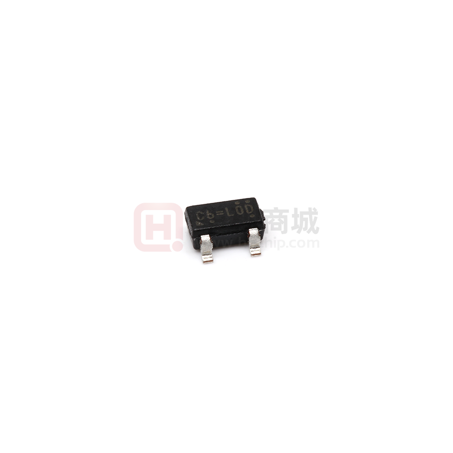
引脚分配:
- SOT-23-3:VIN(2), GND(1), VOUT(3)
- SOT-89:VIN(TAB), GND(2), VOUT(3)
- SOT-223:VIN(2), GND(1), VOUT(3)
- TO-92 (L-Type):VIN(2), GND(1), VOUT(3)
- TO-92 (T-Type):VIN(2), GND(1), VOUT(3)
参数特性:
- 输出电压精度:2%,输入电压范围高达12V
- 线路调节:2%至3%VoUT
- 负载调节:1mV至30/50mV
- 电流限制:350mA至900mA
- 热关机和过热保护
功能详解:
- 内部1.5Ω P-MOSFET,无基极电流
- 极低的接地电流
- 快速瞬态响应
- RoHS合规和100%无铅
应用信息:
- 适用于网络卡、CD-ROM、DVD无线通信系统和电池供电系统
封装信息:
- 提供SOT-23、SOT-89、SOT-223和TO-92封装
- 封装的热阻和最大功耗依赖于环境温度和热阻
典型应用电路:
- 需要在VOUT和GND引脚之间连接10uF电容,以确保稳定性
- 在VIN和GND之间放置1uF或更高电容,以滤除输入噪声
绝对最大额定值:
- 输入电压:-0.3至14V
- 工作结温范围:-40°C至125°C
- 存储温度范围:-65°C至150°C
电气特性:
- 输出电压精度、温度系数、线路和负载调节、电流限制、dropout电压和待机电流等参数均有详细说明。
应用信息:
- 推荐使用10uF电容,ESR大于200mΩ,以避免VOUT振荡
- 铝电解电容在低于-25°C时可能会导致VOUT振荡
- 为了更好的瞬态响应,可以无限增加电容值
热保护:
- 热保护限制了RT9161/A的功耗,当结温超过165°C时,将启动热关机功能