RT9285C
Tiny Package, High Performance, Diode Embedded White
LED Driver
General Description
Features
The RT9285C is a high frequency asynchronous boost
converter with internal diode, which can support 2 to 5
White LEDs for backlighting and OLED power supply. The
Internal soft start function can reduce the inrush current.
The device operates with 1MHz fixed switching frequency
to allow small external components and to simplify possible
EMI problems. The device comes with 20V over voltage
protection to allow inexpensive and small-output capacitors
with lower voltage rating. The LED current is initially set
with the external sense resistor RSET, and the feedback
voltage is 250mV. Tiny package type TSOT-23-6,
XDFN-8L 2x2 and WDFN-8L 2x2 packages provide the best
solution for PCB space saving and total BOM cost.
z
z
z
z
z
z
z
z
z
z
z
Applications
z
Ordering Information
z
RT9285C
z
Lead Plating System
P : Pb Free
G : Green (Halogen Free and Pb Free)
Z : ECO (Ecological Element with
Halogen Free and Pb free)
Note :
Richtek products are :
`
RoHS compliant and compatible with the current require-
z
z
z
Cellular Phones
Digital Cameras
PDAs and Smart Phones
Porbable Instruments
MP3 Player
OLED Power
Pin Configurations
(TOP VIEW)
GND
LX
NC
PGND
1
2
3
FB
EN
VOUT
VDD
8
GND
Package Type
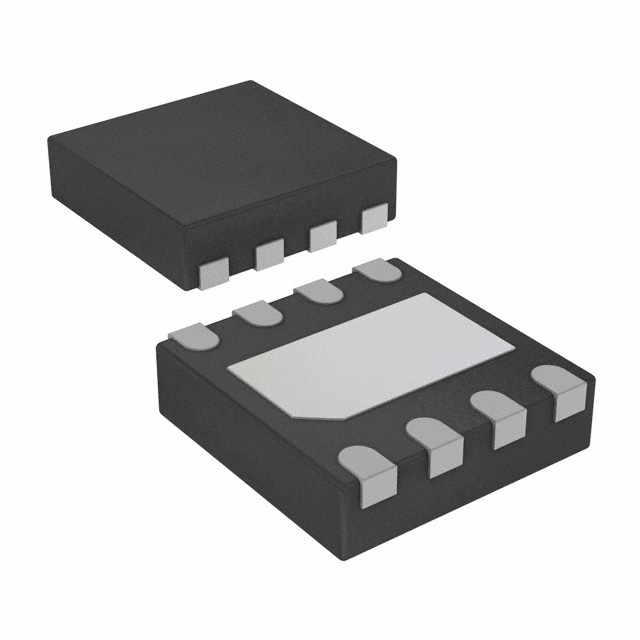
QW : WDFN-8L 2x2 (W-Type)
QX : XDFN-8L 2x2 (X-Type)
J6 : TSOT-23-6
VIN Operating Range : 2.7V to 5.5V
Up to 85% Efficiency
22V Internal Power NMOS
1MHz Switching Frequency
Built-in Diode
Digital Dimming with Zero-Inrush
Input UVLO Protection
Output Over Voltage Protection
Internal Soft Start and Compensation
TSOT-23-6, 8-Lead XDFN and WDFN Package
RoHS Compliant and 100% Lead (Pb)-Free
9
4
7
6
5
XDFN/WDFN-8L 2x2
ments of IPC/JEDEC J-STD-020.
`
Suitable for use in SnPb or Pb-free soldering processes.
VDD VOUT EN
6
Marking Information
For marking information, contact our sales representative
directly or through a Richtek distributor located in your
area.
DS9285C-03
March 2011
LX
5
4
2
3
GND
FB
TSOT-23-6
www.richtek.com
1
�RT9285C
Typical Application Circuit
VIN
2.7V to 5.5V
L1
10µH to 22µH
C1
1µF
RT9285C
VDD
LX
VOUT
EN
C2
0.22µF to 1µF
Chip Enable
GND
FB
RSET
12.5
PGND
PGND pin for XDFN/WDFN-8L Packages
Function Pin Description
Pin No.
XDFN/WDFN-8L TSOT-23-6
1,
Pin Name
Pin Function
Ground Pin. The exposed pad must be soldered to a large PCB and
2
GND
2
1
LX
3
--
NC
No Internal Connection.
4
--
PGND
Power Ground Pin.
5
6
VDD
6
5
VOUT
7
4
EN
9 (Exposed Pad)
connected to GND for maximum power dissipation.
LX Pin. Connect this Pin to an inductor. Minimize the track area to
reduce EMI.
Supply Input Voltage Pin. Bypass 1μF capacitor to GND to reduce the
input ripple.
Output Voltage pin. The pin internally connects to OVP diode to limit
output voltage while LEDs are disconnected.
Chip Enable (Active High). Note that this pin has an internal pull-down
resistance around 300kΩ.
Feedback Pin. Series connecting a resistor between WLED and
8
3
FB
ground as a current sense. Sense the current feedback voltage to set
the current rating.
0.5µs < tHI
EN
Shutdown
IWLED
0
1
0.5µs < tLO < 300µs
2
3
4
100% 15/16
14/16 13/16
12/16
5
14
15
0
1
100%
3/16
2/16
1/16
15/16
Shutdown
Figure 1. Operation of Digital Pulse Dimming Control
www.richtek.com
2
DS9285C-03
March 2011
�RT9285C
Function Block Diagram
1.0MHz OSC
Current
Sense
Slope
Compensation
OCP
LX
PWM
Logic
OVP
VOUT
UVLO/P
GOOD
VDD
EN
FB
VREF
+
Timer
Dimming
Controller
+
-
Soft Start/
Clamping
PGND
GND
Operation
Soft-Start
The Soft-Start function is made by clamping the output
voltage of error amplifier with another voltage source that
is increased slowly from zero to near VIN in the Soft-Start
period. Therefore, the duty cycle of the PWM will be
increased from zero to maximum in this period. The softstart time is decided by a timer of 1.5ms. The charging
time of the inductor will be limited as the smaller duty so
that the inrush current can be reduced to an acceptable
value.
Over Voltage Protection
The Over Voltage Protection is detected by a junction
breakdown detecting circuit. Once VOUT goes over the
detecting voltage, LX pin stops switching and the power
NMOS is turned off. Then, the VOUT is clamped to be near
VOVP.
LED Current Setting
The RT9285C regulates the LED current by setting the
current sense resistor (RSET) connecting to feedback and
ground. The internal feedback reference voltage is 0.25V.
The LED current can be set from following equation easily.
ILED (mA) = 0.25/RSET
DS9285C-03
March 2011
In order to have an accurate LED current, precision resistors
are preferred (1% is recommended). The table for RSET
selection is shown below.
Table 1. RSET Value Selection
ILED (mA)
RSET (Ω)
5
49.9
10
24.9
12
21
15
16.5
20
12.4
Digital Pulse Dimming Control
RT9285C implements the pulse dimming method being
used to control the brightness of white LEDs. There are
16 steps to set the current of white LEDs. The maximum
LED current is up to 20mA that is sufficient for most
application in backlight. The detail operation of brightness
dimming is showed in the Figure 1.
Current Limiting
The current flow through the inductor as charging period is
detected by a current sensing circuit. As the value over
the current limiting, the NMOS will be turned-off so that
the inductor will be forced to leave charging stage and
enter discharging stage. Therefore, the inductor current
will not increase over the current limiting.
www.richtek.com
3
�RT9285C
Absolute Maximum Ratings
(Note 1)
Supply Voltage, VIN --------------------------------------------------------------------------------------------------- −0.3 to 6V
LX Input Voltage ------------------------------------------------------------------------------------------------------- − 0.3V to 22V
z Output Voltage --------------------------------------------------------------------------------------------------------- − 0.3V to 21V
z The other pins ---------------------------------------------------------------------------------------------------------- − 0.3V to 6V
z Power Dissipation, PD @ TA = 25°C
TSOT23-6 --------------------------------------------------------------------------------------------------------------- 0.392W
XDFN/WDFN-8L 2x2 -------------------------------------------------------------------------------------------------- 0.606W
z Package Thermal Resistance (Note 2)
TSOT23-6, θJA ---------------------------------------------------------------------------------------------------------- 255°C/W
XDFN/WDFN-8L 2x2, θJA --------------------------------------------------------------------------------------------- 165°C/W
XDFN/WDFN-8L 2x2, θJC -------------------------------------------------------------------------------------------- 20°C/W
z Junction Temperature ------------------------------------------------------------------------------------------------- 150°C
z Lead Temperature (Soldering, 10 sec.) --------------------------------------------------------------------------- 260°C
z Storage Temperature Range ---------------------------------------------------------------------------------------- − 65°C to 150°C
z
z
Recommended Operating Conditions
z
z
(Note 3)
Junction Temperature Range ---------------------------------------------------------------------------------------- −40°C to 125°C
Ambient Temperature Range ---------------------------------------------------------------------------------------- −40°C to 85°C
Electrical Characteristics
(VIN = 3.7V, FREQ left floating, TA = 25°C, Unless Otherwise specification)
Parameter
Min
Typ
Max
Unit
V IN
2.7
--
5.5
V
Under Voltage Lock Out
V UVLO
1.7
2
2.3
V
Quiescent Current
Supply Current
IQ
IIN
FB = 1.5V, No switch
FB = 0V, Switch
---
300
--
450
2
μA
mA
Shut Down Current
ISHDN
V EN < 0.4V
--
2
5
μA
V IN = 3V to 4.3V
--
--
3
%
--
1
--
MHz
85
90
--
%
0.237
0.25
0.263
V
--
0.9
--
V
0.5
0.75
1
Ω
---
20
400
---
V
mA
System Supply Input
Operation voltage Range
Symbol
Output
Line Regulation
Oscillator
Operation Frequency
Test Conditions
fOSC
Maximum Duty Cycle
Reference Voltage
Feedback Reference Voltage
Diode
V REF
Forward Voltage
V FW
MOSFET
On Resistance of MOSFET
RDS(ON)
Protection
OVP Threshold
OCP
VOVP
IFW = 100mA
To be continued
www.richtek.com
4
DS9285C-03
March 2011
�RT9285C
Parameter
Symbol
Test Conditions
Min
Typ
Max
--
--
0.4
1.4
--
--
Unit
Control Interface
EN Threshold
Logic-Low Voltage
VIL
Logic-High Voltage VIH
V
EN Low Time for Dimming
TLO
Refer to Figure 1
0.5
--
300
μs
Delay Between Steps Time
THI
Refer to Figure 1
0.5
--
--
μs
EN Low Time for Shut Down
TSHDN
Refer to Figure 1
1
--
--
ms
Note 1.Stresses listed as the above "Absolute Maximum Ratings" may cause permanent damage to the device. These are for
stress ratings. Functional operation of the device at these or any other conditions beyond those indicated in the
operational sections of the specifications is not implied. Exposure to absolute maximum rating conditions for extended
periods may remain possibility to affect device reliability.
Note 2. θJA is measured in the natural convection at T A = 25°C on a low effective thermal conductivity test board of
JEDEC 51-3 thermal measurement standard.
Note 3. The device is not guaranteed to function outside its operating conditions.
DS9285C-03
March 2011
www.richtek.com
5
�RT9285C
Typical Operating Characteristics
OVP vs. Input Voltage
Efficiency vs. Input Voltage
20.8
90
20.4
85
80
Efficiency (%)
20
OVP (V)
4W-LED
19.6
19.2
18.8
75
70
65
60
18.4
55
18
50
2.8
3.1
3.4
3.7
4
4.3
4.6
4.9
5.2
5.5
2.8
3.1
3.4
3.7
4.6
4.9
5.2
5.5
5.2
5.5
Frequency vs. Input Voltage
Quiescent Current vs. Input Voltage
450
1.02
400
1.00
-40°C
350
Frequency (MHz)
Quiescent Current (uA)
4.3
Input Voltage (V)
Input Voltage (V)
25°C
300
85°C
250
200
150
0.98
0.96
0.94
0.92
0.90
0.88
100
2.8
3.1
3.4
3.7
4
4.3
4.6
4.9
5.2
5.5
2.8
3.1
3.4
3.7
4
4.3
4.6
4.9
Input Voltage (V)
Input Voltage (V)
Output Voltage vs. Output Current
Enable Voltage vs. Input Voltage
17
0.84
0.83
16
Enable Voltage
0.82
Output Voltage (V)
Enable Voltage (V)
4
0.81
0.80
0.79
0.78
Shutdown Voltage
0.77
0.76
15
14
13
12
11
0.75
10
0.74
2.8
3.1
3.4
3.7
4
4.3
4.6
Input Voltage (V)
www.richtek.com
6
4.9
5.2
5.5
5
15
25
35
45
55
65
75
Output Current (mA)
DS9285C-03
March 2011
�RT9285C
Feedback Reference Voltage vs. Input Voltage
Dimming Operation @ Decreace
Feedback Reference Voltage (mV)
253.5
VIN
(2V/Div)
VOUT
(5V/Div)
253.0
252.5
VIN = 3.7V
252.0
251.5
251.0
EN
(2V/Div)
250.5
250.0
ILED
(10mA/Div)
249.5
249.0
2.8
3.1
3.4
3.7
4
4.3
4.6
4.9
5.2
5.5
Time (500μs/Div)
Input Voltage (V)
Inrush Current Response
VIN
(2V/Div)
VIN = 3.7V
VOUT
(5V/Div)
EN
(2V/Div)
IIN
(100mA/Div)
Time (500μs/Div)
DS9285C-03
March 2011
www.richtek.com
7
�RT9285C
Application Information
LED Current Control
Capacitor Selection
The RT9285C regulates the LED current by setting the
current sense resistor (RSET ) connecting to feedback and
ground. The RT9284A/B feedback voltage (VFB) is 0.25V.
The LED current (ILED) can be set by a resistor RSET .
Input and output ceramic capacitors of 1µF are recommended for RT9285C applications. For better voltage filtering,
ceramic capacitors with low ESR are recommended. X5R
and X7R types are suitable because of their wider voltage
and temperature ranges.
ILED = 0.25/RSET
In order to have an accurate LED current, a precision resistor
is preferred (1% is recommended).
L1
10µH to 22µH
RT9285C
LX
VIN
2.7V to 5.5V
Output Voltage Control
The output voltage of R9285C can be adjusted by the divider
circuit on FB pin. Figure 5 shows a 2-level voltage control
circuit for OLED application. The output voltage can be
calculated by the following equations in Figure 5.
C1
1µF
L1
10µH to 22µH
VDD
EN
VOUT
Chip Enable
GND
C2
0.22µF to 1µF
LX
RSET
12.5
Figure 2. Application for Driving 4 Series WLEDs
RT9285C
LX
EN
VOUT
VDD
VOUT
EN
Chip Enable
GND
R1
590k
C2
0.22µF to 1µF
FB
R2
10k
R1 + R2
VOUT = 0.25 ×
; R2 > 10k
R2
Figure 4. Application for Constant Output Voltage
C1
1µF
GPIO
VIN
VDD
Chip Enable
GND
VIN
2.7V to 5.5V
VOUT
15V
C1
1µF
RT9285C
FB
L1
10µH to 22µH
VIN
2.7V to 5.5V
RT9285C
VDD
C2
0.22µF to 1µF
VOUT
RA R
GPIO
FB
RSET
12.5
LX
FB
EN
GND
OLED
RB
VEN
Figure 3. Application for Driving 5 Series WLEDs
Inductor Selection
The recommended value of inductor for 4 to 5WLEDs
applications are 10µH to 22µH. For 3W LEDs, the
recommended value of inductor is 4.7µH to 22µH. Small
size and better efficiency are the major concerns for portable
device, such as RT9285C used for mobile phone. The
inductor should have low core loss at 1MHz and low DCR
for better efficiency.
The inductor saturation current rating should be considered
to cover the inductor peak current.
www.richtek.com
8
Figure 5. Application Circuit for Output Voltage Control
and Related Equations
VOUT = RA x {(FB/RB) + (FB-GPIO)/RGPIO} + FB
(1)
As GPIO = 0V,
VOUT = RA x {(0.25/RB) + (0.25/RGPIO)} + 0.25
(2)
As GPIO = 2.8V,
VOUT = RA x {(0.25/RB) + (0.25-2.8)/RGPIO )} + 0.25
(3)
DS9285C-03
March 2011
�RT9285C
As GPIO = 1.8V, VOUT = RA x {(0.25/RB) + (0.25-1.8)/
RGPIO)} + 0.25
(4)
For Efficiency Consideration :
Set RA = 990kΩ,
If 2 levels are 16V (GPIO = 0V) and 14V (GPIO = 1.8V)
Get RB = 16kΩ, RGPIO = 890kΩ
Table 2. Suggested Resistance for Output Voltage
Control
Conditions
RA
RB
RGPIO
(kΩ)
(kΩ)
(kΩ)
Case A :
Normal Voltage = 16V
(GPIO = 0V)
1100
18
495
Dimming Voltage = 12V
(GPIO = 1.8V)
temperature of the die (125°C) and TA is the maximum
ambient temperature. The junction to ambient thermal
resistance θJA is layout dependent. For XDFN/WDFN 2x2
packages, the thermal resistance θJA is 165°C/W on the
standard JEDEC 51-3 single layer thermal test board. The
maximum power dissipation at TA = 25°C can be calculated
by following formula:
PD(MAX) = (125°C − 25°C) / (165°C/W) = 0.606 W for WDFN/
XDFN 2x2 packages
PD(MAX) = (125°C − 25°C) / (255°C/W) = 0.392 W for TSOT23-6 packages
The maximum power dissipation depends on operating
ambient temperature for fixed T J (MAX) and thermal
resistance θJA. For RT9285C packages, the Figure 6 of
derating curves allows the designer to see the effect of
rising ambient temperature on the maximum power
allowed.
Case B :
Maximum Power Dissipation (W)
0.8
Normal Voltage = 16V
(GPIO = 0V)
1200
19.5
840
Dimming Voltage = 12V
(GPIO = 2.8V)
Considering the output voltage deviation from the GPIO
voltage tolerance, as GPIO voltage vibrated by 0 ± 50mV
and 1.8(2.8) ±5% ,the output voltage could be kept within
±2.5%.
0.7
0.6
0.5
XDFN/WDFN-8L 2x2
0.4
TSOT-23-6
0.3
0.2
0.1
0
0
Thermal Considerations
For continuous operation, do not exceed absolute
maximum operation junction temperature. The maximum
power dissipation depends on the thermal resistance of
IC package, PCB layout, the rate of surroundings airflow
and temperature difference between junction to ambient.
The maximum power dissipation can be calculated by
following formula:
PD(MAX) = ( TJ(MAX) - TA ) / θJA
Where T J(MAX) is the maximum operation junction
temperature 125°C, TA is the ambient temperature and
the θJA is the junction to ambient thermal resistance.
For recommended operating conditions specification of
RT9285C, where T J (MAX) is the maximum junction
DS9285C-03
March 2011
25
50
75
100
125
Ambient Temperature (°C)
Figure 6. Derating Curves for RT9285C Packages
Layout guide
}
A full GND plane without gap break.
}
Traces in bold need to be routed first and should be
kept as short as possible.
}
VDD to GND noise bypass : Short and wide connection
for the 1µF MLCC capacitor between Pin 6 and Pin 2.
}
LX node copper area should be minimized for reducing
EMI. (*1)
}
The input capacitor C1 should be placed as closed as
possible to Pin 6. (*2)
www.richtek.com
9
�RT9285C
`
The output capacitor C2 should be connected directly
from the Pin 5 to ground rather than across the LEDs.
(*3)
`
FB node copper area should be minimized and keep far
away from noise sources (Pin 1, Pin 5, Pin 6). (*4)
`
The Inductor is far away receiver and microphone.
`
The voice trace is far away RT9285C.
`
The embedded antenna is far away and different side
RT9285C.
`
R1 should be placed as close as RT9285C.
`
The through hole of RT9285C's GND pin is recommended
as large and many as possible.
L1
VIN
C1
*1
*2
LX
1
6
VDD
GND
2
5
VOUT
3
4
EN
C2
*3
GND
RSET
WLEDs
*4
FB
EN
Figure 7. TOP
Figure 8. Bottom
www.richtek.com
10
DS9285C-03
March 2011
�RT9285C
Outline Dimension
H
D
L
C
B
b
A
A1
e
Dimensions In Millimeters
Dimensions In Inches
Symbol
Min
Max
Min
Max
A
0.700
1.000
0.028
0.039
A1
0.000
0.100
0.000
0.004
B
1.397
1.803
0.055
0.071
b
0.300
0.559
0.012
0.022
C
2.591
3.000
0.102
0.118
D
2.692
3.099
0.106
0.122
e
0.838
1.041
0.033
0.041
H
0.080
0.254
0.003
0.010
L
0.300
0.610
0.012
0.024
TSOT-23-6 Surface Mount Package
DS9285C-03
March 2011
www.richtek.com
11
�RT9285C
D2
D
L
E2
E
1
e
SEE DETAIL A
b
2
1
2
1
A
A1
A3
DETAIL A
Pin #1 ID and Tie Bar Mark Options
Note : The configuration of the Pin #1 identifier is optional,
but must be located within the zone indicated.
Dimensions In Millimeters
Dimensions In Inches
Symbol
Min
Max
Min
Max
A
0.700
0.800
0.028
0.031
A1
0.000
0.050
0.000
0.002
A3
0.175
0.250
0.007
0.010
b
0.200
0.300
0.008
0.012
D
1.950
2.050
0.077
0.081
D2
1.000
1.250
0.039
0.049
E
1.950
2.050
0.077
0.081
E2
0.400
0.650
0.016
0.026
e
L
0.500
0.300
0.020
0.400
0.012
0.016
W-Type 8L DFN 2x2 Package
www.richtek.com
12
DS9285C-03
March 2011
�RT9285C
D2
D
L
E
E2
1
e
SEE DETAIL A
b
2
1
2
1
A
A1
A3
DETAIL A
Pin #1 ID and Tie Bar Mark Options
Note : The configuration of the Pin #1 identifier is optional,
but must be located within the zone indicated.
Dimensions In Millimeters
Dimensions In Inches
Symbol
Min
Max
Min
Max
A
0.400
0.500
0.016
0.020
A1
0.000
0.050
0.000
0.002
A3
0.102
0.152
0.004
0.006
b
0.200
0.300
0.008
0.012
D
1.950
2.050
0.077
0.081
D2
1.000
1.250
0.039
0.049
E
1.950
2.050
0.077
0.081
E2
0.400
0.650
0.016
0.026
e
L
0.500
0.300
0.020
0.400
0.012
0.016
X-Type 8L DFN 2x2 Package
Richtek Technology Corporation
Richtek Technology Corporation
Headquarter
Taipei Office (Marketing)
5F, No. 20, Taiyuen Street, Chupei City
5F, No. 95, Minchiuan Road, Hsintien City
Hsinchu, Taiwan, R.O.C.
Taipei County, Taiwan, R.O.C.
Tel: (8863)5526789 Fax: (8863)5526611
Tel: (8862)86672399 Fax: (8862)86672377
Email: marketing@richtek.com
Information that is provided by Richtek Technology Corporation is believed to be accurate and reliable. Richtek reserves the right to make any change in circuit design,
specification or other related things if necessary without notice at any time. No third party intellectual property infringement of the applications should be guaranteed
by users when integrating Richtek products into any application. No legal responsibility for any said applications is assumed by Richtek.
DS9285C-03
March 2011
www.richtek.com
13
�


 工商网监
湘ICP备2023018690号
工商网监
湘ICP备2023018690号