RT9301
3-Channel Low Dropout RGB LED Driver
General Description
Features
The RT9301 is a 3-Channel current source driver for RGB
LED. It is easy to be designed in applications that need
mixing RGB light source for multi-color output.
z
Input Voltage Range : 2.8V to 5.5V
z
Low 60/45mV Dropout at 20/15mA
Individual Current Setting by External Resistor
Individual On/Off Control by Baseband MPU
Up to 50mA LED Bias Current
Simple LED Brightness Control
5%(max.) LED Current Matching
Low 0.1uA Shutdown Current
UVLO Protection
RoHS Compliant and 100% Lead (Pb)-Free
z
z
z
z
z
z
z
Applications
z
Ordering Information
z
RT9301
z
WDFN-8L 3x3 is in W-Type
z
Richtek products are :
8
7
6
5
2
3
4
RoHS compliant and compatible with the current require-
`
Suitable for use in SnPb or Pb-free soldering processes.
LED3
ments of IPC/JEDEC J-STD-020.
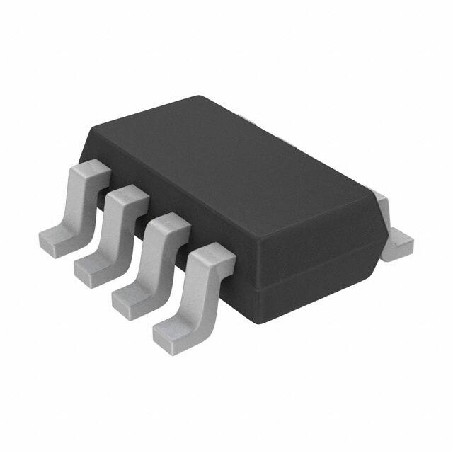
TSOT-23-8
Marking Information
For marking information, contact our sales representative
directly or through a Richtek distributor located in your
area.
GND
`
ISET2
z
(TOP VIEW)
ISET3
Note :
Pin Configurations
ISET1
Lead Plating System
P : Pb Free
G : Green (Halogen Free and Pb Free)
z
VIN
Package Type
J8 : TSOT-23-8
QW : WDFN-8L 3x3 (Green Only)
Mobile phone, Smart Phone Multi-color LED Backlight
Camera Flash White LED
LCD Display Modules
Keypad Backlight
LED1
The RT9301 features very low dropout and under voltage
lockout protection. It is available in a space-saving
TSOT-23-8 and WDFN-8L 3x3 packages.
LED2
The RT9301 also provide users with great flexibility and
device performance. It uses externals resistor to set the
bias current for three LEDs, which are matched to
5%(max.). Users can adjust the output current from 2mA
to 50mA by setting the ISET resistor.
z
LED2
LED1
ISET1
ISET2
1
2
8
GND
6
3
4
7
9
5
LED3
GND
VIN
ISET3
WDFN-8L 3x3
DS9301-05 April 2011
www.richtek.com
1
�RT9301
Typical Application Circuit
VBAT
ON
OFF
VIN LED1
RSET1
VSET1
ISET2
RSET3
VSET3
LED2 LED3
ISET1
R SET2
VSET2
GPIO
1uF
RT9301
GND
ISET3
Figure 1. Application circuit for RGB LED
VBAT
1uF
VIN
RSET1
LED1
LED2
LED3
ISET1
RSET2
GPIO
ISET2
RSET3
ISET3
RT9301
GND
Figure 2. Application Circuit for Backlight
VBAT
1uF
RSET1
RSET2
GPIO
RSET3
VIN
LED1 LED2 LED3
ISET1
ISET2
ISET3
RT9301
GND
Figure 3. Application Circuit for Keypad
ILED1 ~ 3 = 800 x ISET1 ~ 3 = 800 x VSET 1 ~ 3 − 0.9V
RSET1 ~ 3
GPIO (V) ILED (mA)
1.8
2.8
www.richtek.com
2
15
20
15
20
RSET (kΩ)
Nearest Standard Values for RSET (kΩ)
48
36
101
76
47.5
36
100
75
DS9301-05 April 2011
�RT9301
Function Block Diagram
VIN
ISET1
UVLO
+
VREF
-
ISET2
LED1
+
VREF
Current Source
-
LED2
LED3
ISET3
+
VREF
-
GND
Functional Pin Description
Pin No.
RT9301□J8
Pin Name
Pin Function
RT9301GQW
RGB or White LED cathode connection pin. 2mA to 50mA C urrent
1
8
LED3
flows into LED. Floating or connection to ground is used to disable
this pin.
2
7,
Exposed Pad (9)
GND
Ground Pin. The exposed pad must be soldered to a large PCB and
connected to GND for maximum pow er dissipation.
3
6
VIN
Power Input Pin.
4
5
ISET3
Current setting for LED3. Connect to GND if not use.
5
4
ISET2
Current setting for LED2. Connect to GND if not use.
6
3
ISET1
Current setting for LED1. Connect to GND if not use.
7
2
LED1
RGB or White LED cathode connection pin. 2mA to 50mA C urrent
flows into LED. Floating or connection to ground is used to disable
this pin.
8
1
LED2
RGB or White LED cathode connection pin. 2mA to 50mA C urrent
flows into LED. Floating or connection to ground is used to disable
this pin.
DS9301-05 April 2011
www.richtek.com
3
�RT9301
Absolute Maximum Ratings
l
l
l
l
l
l
l
l
l
(Note 1)
Supply Input Voltage ------------------------------------------------------------------------------------------------ −0.3V to 6V
LED1,2,3 Pin Voltage ----------------------------------------------------------------------------------------------- −0.3V to VIN + 0.3V
Other I/O Pin Voltages ---------------------------------------------------------------------------------------------- −0.3V to 6V
Power Dissipation, PD @ TA = 25°C
TSOT-23-8 ------------------------------------------------------------------------------------------------------------- 0.382W
WDFN-8L 3x3 --------------------------------------------------------------------------------------------------------- 0.926W
Package Thermal Resistance (Note 2)
TSOT-23-8, θJA ------------------------------------------------------------------------------------------------------- 262°C/W
WDFN-8L 3x3, θJA --------------------------------------------------------------------------------------------------- 108°C/W
WDFN-8L 3x3, θJC --------------------------------------------------------------------------------------------------- 8.2°C/W
Lead Temperature (Soldering, 10 sec.) -------------------------------------------------------------------------- 260°C
Junction Temperature ----------------------------------------------------------------------------------------------- 150°C
Storage Temperature Range --------------------------------------------------------------------------------------- −65°C to 150°C
ESD Susceptibility (Note 3)
HBM (Human Body Mode) ----------------------------------------------------------------------------------------- 2kV
MM (Machine Mode) ------------------------------------------------------------------------------------------------ 200V
Recommended Operating Conditions
l
l
(Note 4)
Junction Temperature Range -------------------------------------------------------------------------------------- −40°C to 125°C
Ambient Temperature Range -------------------------------------------------------------------------------------- −40°C to 85°C
Electrical Characteristics
(VIN = 3.6V, TA = 25°C, Unless Otherwise specification)
Parameter
Test Conditions
Symbol
Input Supply Voltage
VIN
UVLO Threshold
VUVLO_L
Falling
UVLO Hysteresis
Dropout Voltage
Max
Unit
2.8
--
5.5
V
2
2.2
2.4
V
--
100
--
mV
--
40
120
mV
90% of ILED = 16mA
0.8
0.9
1
V
IQ
LED Open, ISET = 20 uA
--
0.5
1
mA
ILED = 16mA
−5
--
+5
%
ILED = 16mA
−5
--
+5
%
All V SET1~3 < 0.25V
--
0.1
2
µA
ILED Matching
ILED Accuracy
Typ
VLED
ISET Reference Voltage
Quiescent Current
Min
ILED
Shutdown current
V SET Enable Threshold
VSET
VSET connect RSET = 47kΩ to ISET
1.3
--
--
V
V SET Disable Threshold
VIL
VSET connect RSET = 47kΩ to ISET
--
--
0.25
V
Note 1. Stresses listed as the above "Absolute Maximum Ratings" may cause permanent damage to the device. These are for
stress ratings. Functional operation of the device at these or any other conditions beyond those indicated in the
operational sections of the specifications is not implied. Exposure to absolute maximum rating conditions for extended
periods may remain possibility to affect device reliability.
Note 2. θJA is measured in the natural convection at TA = 25°C on a low effective single layer thermal conductivity test board of
JEDEC 51-3 thermal measurement standard. The case point of θJC is on the expose pad for the WDFN package.
Note 3. Devices are ESD sensitive. Handling precaution is recommended.
Note 4. The device is not guaranteed to function outside its operating conditions.
www.richtek.com
4
DS9301-05 April 2011
�RT9301
Typical Operating Characteristics
LED Current vs. Input Voltage
LED Current vs. VSET
25
60
Vf1 = 3.02V, Vf2 = 3.06V, Vf3 = 3.17V
RSET = 36k
LED1
LED2
LED Current (mA)
20
LED Current (mA)
RSET = 51k
RSET = 75k
50
15
LED3
10
5
40
30
RSET = 160k
20
RSET = 360k
10
0
0
2
2.5
3
3.5
4
4.5
5
5.5
1
1.5
2
2.5
3
3.5
4
4.5
Input Voltage (V)
VSET (V)
LED Current vs. Temperature
Dimming Operation
20.4
5
5.5
VBAT = 5.0V
ILED = 20mA
20.3
LED Current (mA)
(1V/Div)
20.2
VSET
20.1
20
(10mA/Div)
19.9
19.8
ILED
19.7
-40
-25
-10
5
20
35
50
65
80
95
Time (100μs/Div)
Temperature (°C)
Enable & Shutdown Response
Line Transient Response
VBAT = 5.0V
VBAT = 3.7V to 4.2V, ILED = 20mA
(1V/Div)
(1V/Div)
VSET
(10mA/Div)
VIN
(10mA/Div)
I LED
ILED
Time (50μs/Div)
DS9301-05 April 2011
Time (50μs/Div)
www.richtek.com
5
�RT9301
Applications Information
The RT9301 is a 3-Channel current source driver for RGB
LED or white LEDs. The output current can be controlled
from 2mA to 50mA by adjusting the setting current from
external. It is easy to support a multi-color RGB LED.
The LED current of each channel can be controlled from
2mA to 50mA. It is easy to obtain a multi-color output
by changing the current of ISET1, ISET2, and ISET3
respectively.
60
Input UVLO
VSET2
VSET3
RSET1
RSET2
RSET3
RSET = 75k
40
30
RSET = 160k
20
RSET = 360k
10
1
The LED current is setting by the current of ISET pin. The
LED current of the three channels (LED1, LED2, LED3)
could be set from the ISET (ISET1, ISET2, ISET3) pins
individually. The typical application circuit shows as
Figure 1.
VSET1
RSET = 51k
0
Output Current Setting
VBAT
RSET = 36k
50
LED Current (mA)
The input operating voltage range of the RT9301 is 2.8V to
5.5V. An input capacitor at the VIN pin could reduce ripple
voltage. It is recommended to use a ceramic 1uF or larger
capacitance as the input capacitor. This IC provides an
under voltage lockout (UVLO) function to prevent it from
unstable issue when startup. The UVLO threshold of input
falling voltage is set at 2.1V typically with a hysteresis
0.1V.
1uF
VIN LED1
LED2 LED3
ISET1
ISET2
ISET3
RT9301
GND
1.5
2
2.5
3
3.5
4
4.5
5
5.5
V SET (V)
Figure 2. LED Current Setting
Figure 2 shows the characteristics of ILED vs. VSET . If the
RSET is selected, the LED current could be controlled from
VSET . The voltage of VSET must be higher than 1.3V to
enable the LED. For low LED current application, it is
recommended to use a higher resistance on RSET (for
example: RSET = 360kΩ).
To disable the LED current, the ISET pin should be
connected to ground or floating. For one LED or two LEDs
application, the unused ISET pin should be connected to
GND. In addition, don’ t short VSETx to ISETx pin.
Figure 1. Typical Application Circuit
VBAT
The LED current can be controlled from an external voltage
(VSET ) and a resistor (RSET ) between VSET and ISET pin.
The voltage range of VSET is from 1.3V to 5.5V. The internal
reference voltage at ISET pin is 0.9V typically. LED current
is set as 800 times the current flowing into ISET pin.
Therefore, the LED current can be calculated as the
following equation.
ILED1 ~ 3 = 800 x ISET1 ~ 3 = 800 x
VSET1
VSET2
RSET1
RSET2
1uF
VIN LED1
LED2 LED3
ISET1
ISET2
ISET3
RT9301
GND
VSET1 ~ 3 - 0.9V
RSET1 ~ 3
Figure 3. Application Circuit for Two LEDs
For example, RSET1 = 45kΩ and VSET1 = 1.8V, the current
of LED1 is equal to 16mA.
www.richtek.com
6
DS9301-05 April 2011
�RT9301
GPIO Control
Figure 4 shows an application circuit for backlight with
GPIO. The three setting resistors are connected to GPIO.
The LED current can be controlled by GPIO directly. The
RT9301 provides low dropout voltage and 5% maximum
current matching. It also allows dimming control frequency
up to 10kHz.
Figure 5 shows another application circuit for keypad
backlight with GPIO. There are 9 LEDs operation in parallel.
A battery or a regulated power source drives the LEDs.
Each channel supports three LEDs. The LED brightness
adjustment can be set with proper setting resistor for each
channel and be controlled from GPIO.
Thermal Considerations
VBAT
1uF
RSET1
VIN
LED1
LED2
LED3
ISET1
RSET2
GPIO
RSET3
ISET2
ISET3
RT9301
GND
For continuous operation, do not exceed absolute
maximum operation junction temperature 125°C. The
maximum power dissipation depends on the thermal
resistance of IC package, PCB layout, the rate of
surroundings airflow and temperature difference between
junction to ambient. The maximum power dissipation can
be calculated by following formula :
PD(MAX) = ( TJ(MAX) − TA ) / θJA
Figure 4. Application Circuit for Backlight with GPIO
The LED current can be set at different value with proper
setting resistor. For typical application of GPIO 1.8V/2.8V
and LED current 15mA/20mA, the recommended current
setting resistors are showed as below table.
Table 1. RSET Value Selection
GPIO
(V)
1.8
2.8
ILED
(mA)
RSET Nearest Standard Values for
(kΩ)
RSET (kΩ)
15
48
47.5
20
36
36
15
101
100
20
76
75
For recommended operating conditions specification of
RT9301, where T J(MAX) is the maximum junction
temperature of the die (125°C) and TA is the maximum
ambient temperature. The junction to ambient thermal
resistance θJA is layout dependent. The thermal resistance
θJA for TSOT-23-8 is 262°C/W, and WDFN-8L 3x3 is
108°C/W on the standard JEDEC 51-3 single-layer thermal
test board. The maximum power dissipation at TA = 25°C
can be calculated by following formula :
PD(MAX) = (125°C − 25°C) / (262°C/W) = 0.382W for
TSOT-23-8 packages
PD(MAX)) = (125°C − 25°C) / (108°C/W) = 0.926W for
WDFN-8L 3x3 packages
VBAT
1uF
RSET1
GPIO
Where T J(MAX) is the maximum operation junction
temperature 125°C, TA is the ambient temperature and the
θJA is the junction to ambient thermal resistance.
RSET2
RSET3
The maximum power dissipation depends on operating
ambient temperature for fixed TJ(MAX) and thermal resistance
θJA. For RT9301 packages, the Figure 1 of derating curves
allows the designer to see the effect of rising ambient
temperature on the maximum power allowed.
VIN
LED1 LED2 LED3
ISET1
ISET2
ISET3
RT9301
GND
Figure 5. Application Circuit for Keypad Backlight
DS9301-05 April 2011
www.richtek.com
7
�RT9301
Maximum Power Dissipation (W)
1
All the traces of LED and V IN running from
chip to LEDs should be wide and short to
reduce the parasitic connection resistance.
Single Layer PCB
0.9
0.8
0.7
Input capacitor (C IN)
should be placed
close to LEDs Pin
and connected to
ground plane. The
Anodes of LEDs
must connect to C IN ,
not battery directly.
WDFN-8L 3x3
0.6
0.5
0.4
TSOT-23-8
0.3
0.2
Battery
0.1
0
0
25
50
75
100
LED3
1
8
LED2
GND
2
7
LED1
VIN
3
6
ISET1
ISET3
4
5
ISET2
125
Ambient Temperature (°C)
Ground Plane
Figure 6. Derating Curves for RT9301 Packages
The GND should be connected to a strong
ground plane for heat sinking and noise
protection.
Layout Consideration
For best performance, careful PCB layout is necessary.
Place all peripheral components as close to the IC as
possible. A short connection is highly recommended. The
following guidelines should be strictly followed when
designing a PCB layout for the RT9301.
Figure 7. ecommended PCB Layout of TSOT-23-8
Package
All the traces of LED and VIN running from chip
to LEDs should be wide and short to reduce the
parasitic connection resistance.
1. All the traces of LED and VIN pin running from chip to
LEDs should be wide and short to reduce the parasitic
connection resistance.
2. Input capacitor (CIN) must be placed close to LEDs and
connected to ground plane. The anodes of LEDs must
be connected to CIN, not battery directly.
LED2
1
8
LED3
LED1
2
7
GND
ISET1
ISET2
3
6
4
5
VIN
ISET3
Input capacitor
(CIN) should
be placed close to
LEDs Pin and
connected to
ground plane. The
Anodes of LEDs
must connect to
CIN, not battery
directly.
Battery
3. Current setting resistors RSET should be placed as close
to the chip as possible.
4. The GND should be connected to a strong ground plane
for heat sinking and noise protection.
5. The current setting resistors should be placed as close
to the IC as possible.
www.richtek.com
8
Grand Plane
The GND should be connected to a strong
ground plane for heat sinking and noise
protection.
Figure 8. Recommended PCB Layout of WDFN-8L 3x3
Package
DS9301-05 April 2011
�RT9301
Outline Dimension
H
D
L
C
B
b
A
A1
e
Dimensions In Millimeters
Dimensions In Inches
Symbol
Min
Max
Min
Max
A
0.700
1.000
0.028
0.039
A1
0.000
0.100
0.000
0.004
B
1.397
1.803
0.055
0.071
b
0.220
0.380
0.009
0.015
C
2.591
3.000
0.102
0.118
D
2.692
3.099
0.106
0.122
e
0.585
0.715
0.023
0.028
H
0.080
0.254
0.003
0.010
L
0.300
0.610
0.012
0.024
TSOT-23-8 Surface Mount Package
DS9301-05 April 2011
www.richtek.com
9
�RT9301
D2
D
L
E2
E
1
e
SEE DETAIL A
b
2
1
2
1
A
A1
A3
DETAIL A
Pin #1 ID and Tie Bar Mark Options
Note : The configuration of the Pin #1 identifier is optional,
but must be located within the zone indicated.
Dimensions In Millimeters
Dimensions In Inches
Symbol
Min
Max
Min
Max
A
0.700
0.800
0.028
0.031
A1
0.000
0.050
0.000
0.002
A3
0.175
0.250
0.007
0.010
b
0.200
0.300
0.008
0.012
D
2.950
3.050
0.116
0.120
D2
2.100
2.350
0.083
0.093
E
2.950
3.050
0.116
0.120
E2
1.350
1.600
0.053
0.063
e
L
0.650
0.425
0.026
0.525
0.017
0.021
W-Type 8L DFN 3x3 Package
Richtek Technology Corporation
Richtek Technology Corporation
Headquarter
Taipei Office (Marketing)
5F, No. 20, Taiyuen Street, Chupei City
5F, No. 95, Minchiuan Road, Hsintien City
Hsinchu, Taiwan, R.O.C.
Taipei County, Taiwan, R.O.C.
Tel: (8863)5526789 Fax: (8863)5526611
Tel: (8862)86672399 Fax: (8862)86672377
Email: marketing@richtek.com
Information that is provided by Richtek Technology Corporation is believed to be accurate and reliable. Richtek reserves the right to make any change in circuit design,
specification or other related things if necessary without notice at any time. No third party intellectual property infringement of the applications should be guaranteed
by users when integrating Richtek products into any application. No legal responsibility for any said applications is assumed by Richtek.
www.richtek.com
10
DS9301-05 April 2011
�


 工商网监
湘ICP备2023018690号
工商网监
湘ICP备2023018690号
