RT9373A
3-Channel Charge Pump White LED Driver with Low
Dropout Current Source
General Description
Features
The RT9373A is a high efficiency and cost effective charge
pump white LED driver. It supports up to 3 white LEDs
with regulated constant current for uniform intensity. The
RT9373A maintains the highest efficiency by utilizing a
x1/x1.5/x2 charge pump and low dropout current
regulators.
z
Very High Efficiency Over 80% of Battery Life
z
Support up to 3 White LEDs
Support Up to 60mA Output Current
1% Typical LED Current Matching
Soft Start Function
Auto Charge Pump Mode Selection
250kHz Fixed Frequency Oscillator
Output Over Voltage Protection
16 Steps Brightness Control
Low Input Noise and EMI
RoHS Compliant and 100% Lead (Pb)-Free
z
z
z
z
z
z
z
z
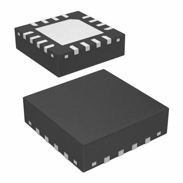
RT9373A is available in a WQFN3x3-16L package.
Applications
Ordering Information
z
Pin Configurations
Richtek products are :
RoHS compliant and compatible with the current requirements of IPC/JEDEC J-STD-020.
`
Suitable for use in SnPb or Pb-free soldering processes.
Marking Information
For marking information, contact our sales representative
directly or through a Richtek distributor located in your
area.
DS9373A-04 April 2011
16 15 14 13
NC
NC
GND
C1P
1
12
2
11
3
10
17
4
9
5
6
7
8
VOUT
`
VIN
Note :
LED2
LED1
(TOP VIEW)
C1N
Lead Plating System
P : Pb Free
G : Green (Halogen Free and Pb Free)
z
LED3
Package Type
QW : WQFN-16L 3x3 (W-Type)
z
VIN
RT9373A
Mobile Phone, DSC, MP3
White LED Backlighting
LCD Display Supply
C2N
User can easily configure each LED current from 1.25mA
to 20mA by a pulse dimming control. The dimming of white
LEDs current can be achieved by applying a pulse signal
to the EN pin. There are totally 16 steps of current could
be set by users.
z
EN
NC
GND
C2P
WQFN-16L 3x3
www.richtek.com
1
�RT9373A
Typical Application Circuit
C PUMP2
1uF
V CC
2.8V to 5.5V
5, 13
C IN
2.2uF
12
GPIO
9
6
C2N
7
C1N
C1P
4
C2P
C PUMP1
1uF
VOUT
VIN
RT9373A
EN
LED3
LED2
LED1
3, 10 GND
8
C OUT
2.2uF
16
15
14
Figure 1. For 3-WLEDs Application Circuit
V CC
2.8V to 5.5V
GPIO
5, 13
C IN
2.2uF
12
9
6
C2N
7
C1N
C1P
4
C PUMP2
1uF
C2P
C PUMP1
1uF
VIN
EN
VOUT
RT9373A
LED3
8
C OUT
2.2uF
16
LED2 15
3, 10 GND
LED1 14
Figure 2. For 2-WLEDs Application Circuit
www.richtek.com
2
DS9373A-04 April 2011
�RT9373A
Functional Pin Description
Pin No.
Pin Name
1, 2, 11,
NC
17 (Exposed Pad)
Pin Function
No Internal Connection.
3
GND
Ground.
4
C1P
Positive Terminal of Bucket Capacitor 1
5
VIN
Power Input Voltage.
6
C2N
Negative Terminal of Bucket Capacitor 2.
7
C1N
Negative Terminal of Bucket Capacitor 1.
8
VOUT
Output Voltage Source.
9
C2P
Positive Terminal of Bucket Capacitor 2.
10
GND
Ground.
12
EN
Chip Enable (Active High). Note that this pin is high impedance.
13
VIN
Power Input Voltage.
14
LED 1
Output Current for LED1. (If not in use, pin should be connected to GND).
15
LED 2
Output Current for LED2. (If not in use, pin should be connected to GND).
16
LED 3
Output Current for LED3. (If not in use, pin should be connected to GND).
C2N
x1/x1.5/x2
Charge Pump
VIN
UVLO
Shut Down Delay
(2ms)
EN
C2P
C1N
C1P
Function Block Diagram
VOUT
Current
Limitation
Soft Start
Circuit
16 Steps Pulse
Dimming Controller
Low Drop Out Current
Source (PMOS)
LED3
LED2
LED1
GND
DS9373A-04 April 2011
www.richtek.com
3
�RT9373A
Absolute Maximum Ratings
z
z
z
z
z
z
z
z
(Note 1)
Supply Input Voltage -----------------------------------------------------------------------------------------------------Other I/O Pin Voltage ----------------------------------------------------------------------------------------------------Power Dissipation, PD @ TA = 25°C
WQFN-16L 3x3 -----------------------------------------------------------------------------------------------------------Package Thermal Resistance (Note 2)
WQFN-16L 3x3, θJA ------------------------------------------------------------------------------------------------------Junction Temperature ----------------------------------------------------------------------------------------------------Lead Temperature (Soldering, 10 sec.) ------------------------------------------------------------------------------Storage Temperature Range -------------------------------------------------------------------------------------------ESD Susceptibility (Note 3)
HBM (Human Body Mode) ---------------------------------------------------------------------------------------------MM (Machine Mode) ------------------------------------------------------------------------------------------------------
Recommended Operating Conditions
z
z
−0.3V to 6V
−0.3V to 6V
1.47W
68°C/W
150°C
260°C
−40°C to 150°C
2kV
200V
(Note 4)
Junction Temperature Range -------------------------------------------------------------------------------------------- −40°C to 125°C
Ambient Temperature Range -------------------------------------------------------------------------------------------- −40°C to 85°C
Electrical Characteristics
(VIN = 2.5V to 5.5V, CIN = COUT = CFLY = 1uF (ESR = 30mΩ), TA = 25°C, unless otherwise specification)
Parameter
Symbol
Test Condition
Min
Typ
Max
Units
2.8
--
5.0
V
1.6
2.1
2.5
V
--
100
--
mV
0.5
1
2
mA
1.5
2.5
5
mA
0
0.1
10
uA
VTS_x1.5 VF = 3.5V, IOUT = 80mA, ILEDx = 20mA
--
3.75
--
V
VF = 3.5V, IOUT = 80mA, ILEDx = 20mA
--
3.0
--
V
--
150
--
mV
1.25
--
20
mA
ILED-ERR 100% Setting
−8
--
+8
%
100% Setting
−5
--
+5
%
1.5
--
--
V
--
--
0.4
V
Input
Input Supply Voltage
VIN
Under-Voltage Lockout
Threshold
Under-Voltage Lockout
Hysteresis
VIN Rising
Quiescent of x1 Mode
IQ_x1
Quiescent of x2 Mode
IQ_x2
Shutdown Current
x1 mode to x1.5 mode
Transition Voltage (V IN Falling)
x1.5 mode to x2 mode
Transition Voltage (V IN Falling)
Hysteresis of Mode Transition
x1 Mode, No Load, All LED pins
connected to GND, VIN = 4V
x2 Mode, No Load, All LED pins floating,
VIN = 3.5V
Enable = 0.4V, V IN = 2.8V to 5.5V
VTS_x2
Output
Current Range of ILEDx
ILEDx Accuracy
2.8 < V IN < 5.5@V F = 3.2, IOUT = 60mA
Current Matching
Enable
Logic-High Voltage V IH
EN
Threshold Logic-Low Voltage V IL
To be continued
www.richtek.com
4
DS9373A-04 April 2011
�RT9373A
Parameter
Symbol
Test Condition
Min
Typ
Max
Units
EN Low Time for Dimming
TIL
0.5
--
500
us
EN High Time for Dimming
TIH
0.5
--
--
us
EN Current
High Current
IIH
V IH = V IN
--
1
10
uA
Low Current
IIL
V IL = GND
--
1
10
uA
TSHDN
Pulse Dimming
--
2
--
ms
--
250
--
kHz
EN Low Time for Shut Down
Frequency
Oscillator Frequency
fOSC
Note 1. Stresses listed as the above "Absolute Maximum Ratings" may cause permanent damage to the device. These are for
stress ratings. Functional operation of the device at these or any other conditions beyond those indicated in the
operational sections of the specifications is not implied. Exposure to absolute maximum rating conditions for extended
periods may remain possibility to affect device reliability.
Note 2. θJA is measured in the natural convection at T A = 25°C on a low effective thermal conductivity test board of
JEDEC 51-3 thermal measurement standard.
Note 3. Devices are ESD sensitive. Handling precaution is highly recommended.
Note 4. The device is not guaranteed to function outside its operating conditions.
DS9373A-04 April 2011
www.richtek.com
5
�RT9373A
Typical Operating Characteristics
Efficiency vs. Input Voltage
LED Current vs. Input Voltage
21.0
95
VF = 3.2V
VF = 3.3V
90
LED2
LED3
85
20.0
Efficiency (%)
LED Current (mA)
20.5
LED1
19.5
19.0
80
75
70
65
60
18.5
55
18.0
50
2.5
3
3.5
4
4.5
5
2.6
5.5
3
3.4
Input Voltage (V)
4.2
4.6
5
5.4
5.8
Input Voltage (V)
Shutdown Current vs. Input Voltage
Quiescent Current vs. Input Voltage
1.5
4.5
Quiescent Current (mA)
4
Shutdown Current (uA)
3.8
1.2
0.9
0.6
0.3
x2 Mode
3.5
3
2.5
2
x1 Mode
1.5
1
0.5
0
0
2.5
3
3.5
4
4.5
5
5.5
2.6
3.1
Input Voltage (V)
4.1
4.6
5.1
5.6
Input Voltage (V)
Oscillator Frequency vs. Input Voltage
Enable Voltage vs. Input Voltage
300
1.20
EN Voltage Threshold (V)
Oscillator Frequency (kHz)
3.6
250
200
150
100
50
1.15
1.10
1.05
Rising
1.00
0.95
Falling
0.90
0.85
0
0.80
2.5
3
3.5
4
4.5
Input Voltage (V)
www.richtek.com
6
5
5.5
2.5
3
3.5
4
4.5
5
5.5
Input Voltage (V)
DS9373A-04 April 2011
�RT9373A
Dimming Operation
VIN
(2V/Div)
VOUT
(2V/Div)
VIN = 3.3V
Dimming Operation
VIN
(2V/Div)
VOUT
(2V/Div)
EN
(2V/Div)
EN
(2V/Div)
I LED
(20mA/Div)
ILED
(20mA/Div)
Time (1ms/Div)
Time (1ms/Div)
x1 Mode Inrush Current Response
x1.5 Mode Inrush Current Response
VIN
(2V/Div)
VIN
(2V/Div)
VOUT
(5V/Div)
VOUT
(5V/Div)
EN
(2V/Div)
EN
(2V/Div)
IIN
(500mA/Div)
VIN = 3.6V
VIN = 4.2V, CIN = COUT = 2.2uF, CPUMP = 1uF
IIN
(500mA/Div)
VIN = 3.7V, CIN = COUT = 2.2uF, CPUMP = 1uF
Time (25us/Div)
Time (100us/Div)
x2 Mode Inrush Current Response
x2 Mode EN Pin Shutdown Response
VIN = 3V, CIN = COUT = 2.2uF, CPUMP = 1uF
CIN = COUT = 2.2uF, CPUMP = 1uF
C2N
(2V/Div)
VIN
(2V/Div)
VOUT
(5V/Div)
EN
(2V/Div)
VOUT
(5V/Div)
EN
(2V/Div)
ILED
(500mA/Div)
IIN
(500mA/Div)
Time (100us/Div)
DS9373A-04 April 2011
Time (500us/Div)
www.richtek.com
7
�RT9373A
x1.5 Mode Ripple & Spike
x2 Mode Ripple & Spike
VIN = 3.3V, CIN = COUT = 2.2μF
VIN = 3.0V, CIN = COUT = 2.2μF
VIN ac
(100mV/Div)
VIN ac
(100mV/Div)
VOUT ac
(200mV/Div)
VOUT ac
(200mV/Div)
C2N
(2V/Div)
C2N
(2V/Div)
Time (1us/Div)
www.richtek.com
8
Time (1us/Div)
DS9373A-04 April 2011
�RT9373A
Applications Information
20mA that is sufficient for most application in backlight.
The dimming of white LEDs' current can be achieved by
applying a pulse signal to the EN pin. There are totally 16
steps of current could be set by users. The detail operation
of brightness dimming is showed in the Figure 3.
The RT9373A is a high efficiency charge pump white LED
driver. It provides 3 channels low dropout voltage current
source to regulated 3 white LEDs current. For high
efficiency, the RT9373A implements a smart mode
transition for charge pump operation. The RT9373A
provides pulse dimming function for LED brightness
control.
Selecting Capacitors
To get the better performance of RT9373A, the selecting
of peripherally appropriate capacitor and value is very
important. These capacitors determine some parameters
such as input and output ripple, power efficiency, maximum
supply current by charge pump, and start-up time. To
reduce the input and output ripple effectively, the low ESR
ceramic capacitors are recommended. Generally, to
reduce the output ripple, increasing the output capacitance
COUT is necessary. However, this will increase the startup time of output voltage. For LED driver applications, the
input voltage ripple is more important than output ripple.
Input ripple is controlled by input capacitor CIN, increasing
the value of input capacitance can further reduce the ripple.
Practically, the input voltage ripple depends on the power
supply’ s impedance. If a single input capacitor CIN cannot
satisfy the requirement of application, it is necessary to
add a low-pass filter. C-R-C filter used to reduce input
ripple. The flying capacitor CPUMP1 and CPUMP2 determine
the supply current capability of the charge pump. The lower
value will limit the LED’ s current at low input voltage.
Soft Start
The RT9373A includes a soft start circuit to limit the inrush
current at power on and mode switching. Soft start circuit
limits the input current before output voltage reaching a
desired voltage level. When the soft start off, the RT9373A
won't sink spike current from VIN.
Mode Decision
The RT9373A uses a smart mode decision method to
select the working mode for maximum efficiency. The
charg pump can operation at x1, x1.5 or x2 mode. The
mode decision circuit senses the output and LED voltage
for up/down selection.
Brightness Control
The RT9373A implements the pulse dimming method
being used to control the brightness of white LEDs. The
part implements a 4-bit DAC for brightness control. Users
can easily configure the LED current from 1.25mA to 20mA
by a serial pulse. The maximum LED current is up to
30us < tREADY 0.5us < t
HI
EN
Shutdown
ILEDX
0
1
2
3
2ms < tSHDN
0.5us < tLO < 500us
4
5
100% 15/16
14/16 13/16
12/16
14
15
0
1
100%
2/16 1/16
15/16
Shutdown
Figure 3. Brightness control by pulse dimming. RT9373A implements 16 steps brightness control
DS9373A-04 April 2011
www.richtek.com
9
�RT9373A
Layout Consideration
The RT9373A is a low dropout current source for white LED driver. Careful PCB layout is necessary. For best performance,
place all peripheral components as close to the IC as possible. A short connection is highly recommended. The following
guidelines should be strictly followed when designing a PCB layout for the RT9373A.
1. All the traces of LED pins running from chip to LEDs should be wide and short to reduce the parasitic connection
resistance.
2. Input capacitor (CIN) should be placed close to VIN (Pin 5) and connected to ground plane. The trace of VIN in the PCB
should be placed far away the sensitive devices or shielded by the ground.
3. The GND should be connected to a strong ground plane for heat sinking and noise protection.
4. Output capacitor (COUT) should be placed close to VOUT and connected to ground plane to reduce noise coupling from
charge pump to LEDs.
5. The traces running from pins to flying capacitor should be short and wide to reduce parasitic resistance and prevent
noise radiation.
LED3
LED2
LED1
VIN
16
15
14
13
All the traces of LED pins
running from chip to LEDs
should be wide and short to
reduce the parasitic
connection resistance.
GND
3
10
GND
C1P
4
9
C2P
C1
8
NC
VOUT
11
7
2
C1N
NC
6
EN
C2N
12
5
1
VIN
NC
The traces running from pins
to flying capacitor should be
short and wide to reduce
parasitic resistance and
prevent noise radiation.
C IN
Ground Plane
C2
C OUT
Battery
The GND should be
connected to a strong
ground plane for heat
sinking and noise
protection.
Output capacitor (C OUT )
should be placed close to
V OUT and connected to
ground plane to reduce
noise coupling from
charge pump to LEDs.
Input capacitor (C IN ) should be placed close to V IN
(Pin 5) and connected to ground plane. The trace
of V IN in the PCB should be placed far away the
sensitive devices or shielded by the ground.
Figure 4. PCB Layout Guide
www.richtek.com
10
DS9373A-04 April 2011
�RT9373A
Outline Dimension
D
SEE DETAIL A
D2
L
1
E
E2
e
b
A
A1
1
1
2
2
DETAIL A
Pin #1 ID and Tie Bar Mark Options
A3
Note : The configuration of the Pin #1 identifier is optional,
but must be located within the zone indicated.
Symbol
Dimensions In Millimeters
Dimensions In Inches
Min
Max
Min
Max
A
0.700
0.800
0.028
0.031
A1
0.000
0.050
0.000
0.002
A3
0.175
0.250
0.007
0.010
b
0.180
0.300
0.007
0.012
D
2.950
3.050
0.116
0.120
D2
1.300
1.750
0.051
0.069
E
2.950
3.050
0.116
0.120
E2
1.300
1.750
0.051
0.069
e
L
0.500
0.350
0.020
0.450
0.014
0.018
W-Type 16L QFN 3x3 Package
Richtek Technology Corporation
Richtek Technology Corporation
Headquarter
Taipei Office (Marketing)
5F, No. 20, Taiyuen Street, Chupei City
5F, No. 95, Minchiuan Road, Hsintien City
Hsinchu, Taiwan, R.O.C.
Taipei County, Taiwan, R.O.C.
Tel: (8863)5526789 Fax: (8863)5526611
Tel: (8862)86672399 Fax: (8862)86672377
Email: marketing@richtek.com
Information that is provided by Richtek Technology Corporation is believed to be accurate and reliable. Richtek reserves the right to make any change in circuit
design, specification or other related things if necessary without notice at any time. No third party intellectual property infringement of the applications should be
guaranteed by users when integrating Richtek products into any application. No legal responsibility for any said applications is assumed by Richtek.
DS9373A-04 April 2011
www.richtek.com
11
�


 工商网监
湘ICP备2023018690号
工商网监
湘ICP备2023018690号
