®
RT9467
5A Single Cell Li-Ion Switching Battery Charger with Power
Path Management and USB-OTG Boost Mode
General Description
Features
The RT9467 is a switch-mode single cell Li-Ion/Li-Polymer
battery charger for portable applications. It integrates a
synchronous PWM controller, power MOSFETs, input
current sensing and regulation, high-accuracy voltage
regulation, and charge termination. The charge current is
regulated through integrated sensing resistors. The
RT9467 also features USB On-The-Go (OTG) support.
RT9467 integrates D+/D- pin for USB host/charging port
detection.
The RT9467 optimizes for charging task by using a control
algorithm to vary the charge rate for different modes,
including pre-charge mode, fast charge mode (constant
voltage and constant current). The key charge parameters
are programmable through an I2C interface. The RT9467
will resume the charge cycle whenever the battery voltage
falls below an internal recharge threshold, and can
automatically enter sleep mode if the input power supply
is removed.
Other features include under-voltage protection, over
voltage protection, thermal regulation and reverse leakage
protection.
The RT9467 is available in a WQFN-24L 4x4 package.
Applications
Cellular Telephones
Personal Information Appliances
Tablet PC, Power Bank
Portable Instruments
Ordering Information
RT9467
Package Type
QW : WQFN-24L 4x4 (W-Type)
(Exposed Pad-Option 2)
Lead Plating System
G : Green (Halogen Free and Pb Free)
Note :
Richtek products are :
RoHS compliant and compatible with the current requirements of IPC/JEDEC J-STD-020.
Suitable for use in SnPb or Pb-free soldering processes.
Copyright © 2021 Richtek Technology Corporation. All rights reserved.
DS9467-01 May 2021
High Efficiency 5A, 1.5MHz Switching Charger with
Output Inductor DFE252012F, TOKO
Charging Efficiency 90.25% at ICHG = 2A
Charging Efficiency 88.86% at ICHG = 3A
Charging Efficiency 84.2% at ICHG = 5A
Synchronous 1.5MHz/0.75MHz Fixed-Frequency
PWM Controller with Up to 95% Duty Cycle
Power Path Management by BATFET Control
Support High Voltage Input (9V/12V)
Support High Voltage Input Adapter (Pump Express
1.0/2.0)
Support IR Compensation Function from Charger
Output to Cell Terminal
Optimize Input Sourcing Capability to Prevent
Overload
2
AICR Current Limit Setting via I C
ILIM Pin for Current Limit Setting
Average Input Current Limit Measurement
Shipping Mode for Battery Leakage Reduction
Wake Up System, Exit Shipping Mode, and Reset
System by QON Pin
Automatic Charging
Average Input Current Regulation (AICR) :
0.1A to 3.25A in 50mA Steps
Charge Current Regulation Accuracy : ±7%
Charge Voltage Regulation Accuracy : ±1% (0 to
85°°C)
Protection for Overall System Considerations
Thermal Regulation for Current Reduction and
Over-Temperature Protection
Input Over-Voltage Protection
Input Bad Adapter Protection
Battery Over-Voltage Protection
Support ADC Conversion for
VBUS, VBAT, VSYS, REGN, TS_BAT, IBUS, IBAT,
TEMP_JC
INT Output for Communication with Host Through
I2C (Watch Dog / Polling Function)
is a registered trademark of Richtek Technology Corporation.
www.richtek.com
1
�RT9467
Pin Configuration
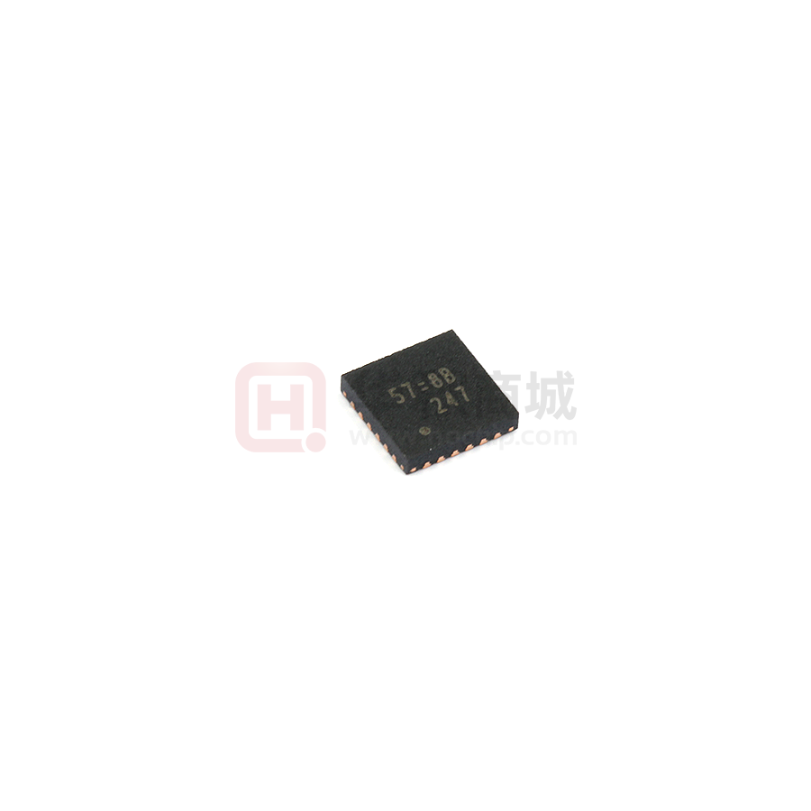
Marking Information
57= : Product Code
DSEL
VMID
REGN
BTST
LX
LX
57=YM
DNN
(TOP VIEW)
YMDNN : Date Code
24 23 22 21 20 19
VBUS
D+
DSTAT
SCL
SDA
1
18
2
17
3
16
PGND
4
15
25
5
14
6
13
8
9 10 11 12
INT
OTG
CEB
ILIM
TS
QON
7
PGND
PGND
SYS
SYS
BAT
BAT
WQFN-24L 4x4
Typical Application Circuit
RT9467
Input
4V to 14V
1
VBUS
BTST
21
47nF
2.2µF
23
LX
VMID
1µH
19, 20
To System
10µF
4.7µF
4.7µF
22
SYS
BAT
4
15, 16
REGN
4.7µF
698 Ω
13, 14
10µF
STAT
10 ILIM
5
2
6
To I C BUS
9
8
2
3
24
10µF
REGN
SCL
TS
SDA
11
Battery
Pack
CEB
OTG
D+
INT
DQON
DSEL
7
12
PGND
17, 18
Below are recommended components information
Pin
Description
Part Number
Package
Manufacturer
VBUS
2.2μF/25V/X5R
GRM155R61E225KE11
0402
muRata
VMID
4.7μF/25V/X5R
GRM188R61E475KE11
0603
muRata
BTST
47nF/16V/X5R
GRM033R61C473KE84
0201
muRata
SYS
10μF/6.3V/X5R
GRM185R60J106ME15
0603
muRata
BAT
10μF/6.3V/X5R
GRM185R60J106ME15
0603
muRata
REGN
4.7μF/6.3V/X5R
GRM155R60J475ME47
0402
muRata
LX
1μH/20%
DFE252012F-1R0
2.5 x 2mm
TOKO
ILIM
698Ω/1%
RR0306S-6980-FNH
0201
CYNTEC
Copyright © 2021 Richtek Technology Corporation. All rights reserved.
www.richtek.com
2
is a registered trademark of Richtek Technology Corporation.
DS9467-01 May 2021
�RT9467
Functional Pin Description
Pin No.
Pin Name
Pin Description
1
VBUS
Power input.
2
D+
USB D+ port.
3
D-
USB D- port.
4
STAT
Charge status indication, open-drain output that indicates charge is in progress
when held low and charge is finished when held High. If any fault occurs,
CHG_STAT will blink at the frequency of 1Hz. Connect a 2.2k-10kΩ pull-up
resistor.
5
SCL
I2C interface serial clock input. Open-drain. An external pull-up resistor is
required.
6
SDA
I2C interface serial data input/output. Open-drain. An external pull-up resistor is
required.
7
INT
Interrupt output, active-low open-drain. Indicator of the charger/Boost event for
system processor.
8
OTG
OTG boost mode enable control, active-high. Act with OTG_PIN_EN
(Addr0x01[1]). (Internal pull down 102kΩ)
9
CEB
Charger enable input, active-low. (Internal pull down 102kΩ)
10
ILIM
Input current limit setting pin. A resistor is connected from ILIM pin to ground to
set the maximum input current limit. The actual input current limit is the lower
value set through the ILIM pin and IAICR register bits.
11
TS
Battery temperature-sense input, connected to a resistor divider for temperature
programming. If there is no need for the battery temperature-sense function, a
50kΩ resistor is connected to REGN and another 50kΩ resistor to ground.
12
QON
Internal BATFET enable control input. In shipping mode, QON is pulled Low for
the duration of tSHIPMODE (typical 0.9s) to exit shipping mode.
13, 14
BAT
Charge current output node for battery connection. The internal BATFET is
connected between VSYS and BAT. Connect a 10μF ceramic capacitor between
BAT and ground.
15, 16
SYS
System connection node. The internal BATFET is connected between SYS and
BAT. Connect a 20μF ceramic capacitor between SYS and ground.
17, 18
PGND
Power ground.
19, 20
LX
Switch node for output inductor connection.
BTST
Bootstrap capacitor connection for high-side gate driver. Connect a capacitor
from BTST to LX to power the internal gate driver.
REGN
Regulated output voltage to supply for the PWM low-side gate driver and the
bootstrap capacitor. Connect a 4.7μF ceramic capacitor from REGN to GND.
1. If VBUS is plugged in, REGN will be powered by VBUS and regulated to
4.9V.
2. If VBUS is unplugged, the charger will operate in sleep mode and the REGN
voltage will be 0V.
* For #2. : Since the REGN voltage is also used to power the TS resistor, when
the charger is in sleep mode, the REGN will be woken up (be reactivated) if
VBAT is greater than forward voltage (VF) of the internal high-side(HS) MOS
diode by VSLEEP_EXIT with all function of the internal ADC being activated and
I2C R/W. The REGN wake-up time is 500ms.
21
22
Copyright © 2021 Richtek Technology Corporation. All rights reserved.
DS9467-01 May 2021
is a registered trademark of Richtek Technology Corporation.
www.richtek.com
3
�RT9467
Pin No.
Pin Name
Pin Description
VMID
Connection point between the reverse blocking MOSFET and the high-side
switching MOSFET.
DSEL
1. Open drain type configuration
2. During input source type detection, the pin drives low.
3. When detection is completed, the pin keeps low. (DCP / HVDCP)
4. When detection is completed, the pin keeps high. (The other type source
detection, SDP /CDP)
25 (Exposed Pad) PGND
Power ground. The exposed pad must be connected to GND and well soldered
to a large PCB copper area for maximum power dissipation.
23
24
Functional Block Diagram
REGN
VBUS
VMID
BTST
LDO
D+
D-
USB Host/
Adapter/Quick
Charge
Detection
UUG
Controller
Charger/OTG
Controller
H/L
Driver
LX
Analog Base
PGND
SYS
VBUS
VSYS
Protection
VBAT
SCL
Power path
Controller
BAT
IBUS
2
I C
SDA
ADC
IBAT
REGN
INT
State Machine
TS
STAT
Silicon Temp
Detection
DSEL
OTG
Copyright © 2021 Richtek Technology Corporation. All rights reserved.
www.richtek.com
4
CEB
ILIM
QON
is a registered trademark of Richtek Technology Corporation.
DS9467-01 May 2021
�RT9467
Operation
The RT9467 is an integrated single cell Li-ion battery
switching charger with power path controller.
Base Circuits
Base circuits provide the internal power, VREGN and
reference voltage and bias current.
Protection Circuits
The protection circuits include the VINOVP, VINUVLO,
BATOVP and OTP circuits. The protection circuits turn
off the charging when the input power or die temperature
is in abnormal level.
TS Detection
The RT9467 detects the temperature of the battery pack
via REGN and TS pins. The REGN pin provides a constant
voltage source to drive the voltage divider composed of a
pulled-high resister and a NTC resister. The RT9467 reports
the sensing results via IRQ and status bits for COLD,
COOL, WARM and HOT.
I2C Controller
The key parameters of charging and OTG are programmable
through I2C commands.
Buck Regulator for Charging and Boost Regulator
as OTG
The multi-loop controller controls the operation of charging
process and current supply to the system. It also controls
the circuits as a Boost converter for OTG applications.
Battery Detection
The RT9467 is capable of doing the battery absence
detection. The detection protects the charger when battery
is removed accidentally.
Adapter Detection
If the poor input power source is connected to the RT9467,
the operation will be shut down by the adapter detection.
Power Path Management and Control
Once the battery voltage increases to a defined system
minimum regulation voltage, the internal path between
SYS and BAT will be fully turned on. That is, a better
charging efficiency can be achieved. When end of charge
occurs, the charging will stop and the internal path will be
turned off.
USB Charger Detection
The RT9467 can detect and distinguish Standard
Downstream Port, Charging Downstream Port and
Dedicated Charging Port via DP and DM pins.
Copyright © 2021 Richtek Technology Corporation. All rights reserved.
DS9467-01 May 2021
is a registered trademark of Richtek Technology Corporation.
www.richtek.com
5
�RT9467
Absolute Maximum Ratings
(Note 1)
Supply Input Voltage, VBUS --------------------------------------------------------------------------------------------Supply Input Voltage, VBUS (Peak