®
RTQ2130B-QT
0.7A, 36V, 2.1MHz Synchronous Small Form Factor StepDown Converter
General Description
Features
The RTQ2130B is a high-efficiency, monolithic
synchronous step-down DC-DC converter that can deliver
up to 0.7A output current from a 3V to 36V widely input
supply. The RTQ2130B current-mode control with external
compensation allows the transient response to be
optimized over various loads and output capacitors. Cycleby-cycle current limit provides protection against shortcircuit output, and soft-start can eliminate input current
surge during startup. Input under-voltage lockout, output
under-voltage protection, over-current protection and overtemperature protection offer completely safe and smooth
operation in all applied conditions. The RTQ2130B is fully
specified over the temperature range of TA = −40°C to 125°C
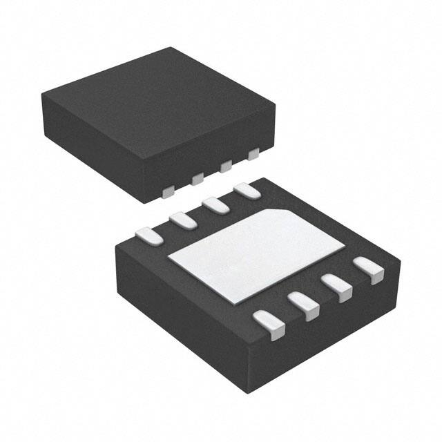
and is available in WDFN-8SL 2x3 package.
Applications
Automotive Systems
Car Camera Module and Car Cockpit Systems
Connected Car Systems
Point of Load Regulator in Distributed Power Systems
Digital Set Top Boxes
Broadband Communications
AEC-Q100 Grade 1 Qualified
Wide Input Voltage Range
4V to 36V
3V to 36V (Soft-start is finished)
99% Duty Cycle Operation
Tight Switching Frequency Variation 2.1MHz ± 10%
Over Operating Ambient Temperature
5V Fixed Output Voltage ( see Ordering Information
for availability)
0.7A Output Current
−40°°C to 125°°C Operating Ambient Temperature
Range
Current-Mode Control
Integrated 200mΩ
Ω/160mΩ
Ω MOSFETs
Enable Control
Over-Temperature Protection
Output Under-Voltage Protection with Hiccup Mode
Adjacent Pin Short-Circuit Protection
Cycle-by-Cycle Over-Current Protection
Input Under-Voltage Lockout
RoHS Compliant and Halogen Free
Ordering Information
RTQ2130B (-
)
Pin Configuration
Grade
QT : AEC-Q100 Qualified
1
2
3
4
PAD
(TOP VIEW)
VIN
BOOT
SW
GND
9
8
7
6
5
-QT
Package Type
QW : WDFN-8SL 2x3 (W-Type)
VCC
EN
FB/VS
COMP
Lead Plating System
G : Green (Halogen Free and Pb Free)
Fixed Output Voltage
50 : 5V
WDFN-8SL 2x3
Note :
Richtek products are :
RoHS compliant and compatible with the current requirements of IPC/JEDEC J-STD-020.
Copyright © 2018 Richtek Technology Corporation. All rights reserved.
DSQ2130B-QT-01 May 2018
Suitable for use in SnPb or Pb-free soldering processes.
is a registered trademark of Richtek Technology Corporation.
www.richtek.com
1
�RTQ2130B-QT
Marking Information
RTQ2130BGQW-QT
RTQ2130B-50GQW-QT
17 : Product Code
1E : Product Code
W : Date Code
17W
1EW
W : Date Code
Functional Pin Description
Pin No.
Pin Name
Pin Function
1
VIN
Supply input. Supply the power to the internal control circuit as well as the
power switches of the device. Drive VIN with a 3V to 36V power source and
bypass VIN to GND with a suitable large capacitor to eliminate noise.
2
BOOT
Bootstrap supply for high-side gate driver. Connect a 100nF or greater
capacitor from SW to BOOT to power the high-side switch.
3
SW
Switch node. SW is the switching node that supplies power to the output and
connect the output LC filter from SW to the output load.
4
GND
System ground. Provide the ground return path for the control circuitry and
low-side power MOSFET.
5
COMP
Compensation node. The current comparator threshold increases with this
control voltage. Connect external compensation elements to this pin to
stabilize the control loop.
6
FB/VS
Output voltage sense. There are two output voltage setting options : one is a
fixed output voltage available for the VS pin, and the other is through a
resistive divider to sense the output voltage at the FB pin. The feedback
reference voltage is 0.8V typically.
7
EN
Enable control input. Connect this pin to logic high can enable the device and
connect this pin to GND can disable the device.
8
VCC
Linear regulator output. VCC is the output of the internal 5V linear regulator
powered by VIN. Decouple with a 1F ceramic capacitor from VCC to ground
for normal operation.
9 (Exposed Pad)
PAD
Exposed pad. The exposed pad is internally unconnected and must be
soldered to a large PCB copper area for maximum power dissipation.
Copyright © 2018 Richtek Technology Corporation. All rights reserved.
www.richtek.com
2
is a registered trademark of Richtek Technology Corporation.
DSQ2130B-QT-01 May 2018
�RTQ2130B-QT
Functional Block Diagram
Adjustable Output Voltage
VCC
VIN
+
EN
Enable
Threshold
Enable
Comparator
0.8V
Current
Sense
BOOT
Power
Stage &
Dead-time
Control
HS Switch
Current
Comparator
+ EA
+
Internal
Regulator
BOOT
UVLO
Logic &
Protection
Control
Fold-back
Control
FB
UVLO
SW
LS Switch
Current
Comparator
Current
Sense
SS
Oscillator
GND
Slope
Compensation
COMP
Fixed 5V Output Voltage
VCC
VIN
+
EN
Enable
Threshold
VS
Enable
Comparator
Fold-back
Control
0.8V
UVLO
BOOT
UVLO
Logic &
Protection
Control
Current
Sense
BOOT
Power
Stage &
Dead-time
Control
HS Switch
Current
Comparator
+ EA
+
Internal
Regulator
SW
LS Switch
Current
Comparator
Current
Sense
SS
GND
Oscillator
Slope
Compensation
COMP
Copyright © 2018 Richtek Technology Corporation. All rights reserved.
DSQ2130B-QT-01 May 2018
is a registered trademark of Richtek Technology Corporation.
www.richtek.com
3
�RTQ2130B-QT
Operation
Switching Frequency and Operational Duty Cycle
Internal Regulator
With normal duty cycle, the RTQ2130B operates at fixed
switching frequency = 2.1MHz. If the duty cycle is too
high/low, in order to extend the operational input voltage
range, the RTQ2130B is forced to lower its switching
frequency by skipping on/off pulses.
The internal regulator generates a 5V regulated voltage,
VCC, to drive internal circuit. When VIN is below 5V, VCC
The minimum on time of the RTQ2130B is 60ns (typ., at
IOUT = 0.5A). If input voltage is too high and the required
on pulse width becomes smaller than minimum on time,
IC starts to skip on pulse once the V(COMP) has reached
its low clamped value.
The minimum off time of the RTQ2130B is 60ns (typ.). If
input voltage drops and the required off pulse width
becomes smaller than minimum off time, IC starts to skip
off pulse and keeps H/S MOSFET on continuously. With
this feature, IC can support > 99% duty cycle.
will track with VIN. A capacitor ( = 1μF), connected from
VCC to GND, is required.
Internal Soft-Start Function
The RTQ2130B provides an internal soft-start function. The
soft-start function is used to prevent large inrush current
while the converter is being powered-up. The typical softstart time (i.e. for the FB voltage to ramp from 0V to 0.8V)
is 2ms.
When voltage of EN pin exceeds threshold voltage, VCC
will start up first and after 0.8ms output voltage ramp up
during soft-start time as shown in Figure 1.
VIN = 12V
VIN
Input Under-Voltage Lockout Threshold
The RTQ2130B includes an input under-voltage lockout
protection (UVLO) circuit. If input voltage exceeds a UVLO
rising threshold voltage (VUVLO), the converter will reset
and prepare the PWM for operation. If the input voltage
falls below a UVLO falling threshold voltage (i.e. VUVLO −
ΔVUVLO) during normal operation, the converter will stop
switching. There is some hysteresis between UVLO rising
and falling threshold voltages to prevent a reset caused
by noise.
Note that V IN = 3V is only design for cold crank
requirement. Normal input voltage should be larger than
UVLO rising threshold to turn on.
Chip Enable
The EN pin is the chip enable input. Pulling the EN pin
low to 1.25V (typ) will disable output voltage and low to
0.4V will shut down the device. During shutdown mode,
the shutdown current of the RTQ2130B is lower than 10μA.
The EN pin has an internal pull-down current source. When
VCC exceeds 5V, the current source typically sinks 1.2μA
for V_EN < 4V and up to 70μA for V_EN > 4V.
Copyright © 2018 Richtek Technology Corporation. All rights reserved.
www.richtek.com
4
VCC = 5V
VCC
EN
0.8ms
2ms
VOUT
Figure 1. Soft-Start Sequence
High-Side MOSFET Over-Current Limit
IC detects the inductor current during the period highside MOSFET turns on. When inductor current reaches
the current limit value, IC will turn off high-side MOSFET,
so it can provide cycle-by-cycle peak current limit
protection to prevent IC from over current.
Low-Side MOSFET Over-Current Limit
The RTQ2130B not only implements the high-side switch
current limit but also provides the low-side switch sourcing
current limit and low-side switch sinking current limit for
low-side MOSFET. With these current protections, the IC
can easily control inductor current at both side power
switches and avoid current runaway for short-circuit
condition.
is a registered trademark of Richtek Technology Corporation.
DSQ2130B-QT-01 May 2018
�RTQ2130B-QT
For the low-side switch sourcing current limit, there is a
specific comparator in internal circuitry to compare the
low-side MOSFET sourcing current to the internal set
current limit at the end of every clock cycle. When the
low-side sourcing current is higher than the set sourcing
limit, the high-side power switch is not turned on and lowside power switch is kept on until the following clock cycle
for releasing the above sourcing current to the load. It is
allowed to turn on the high-side MOSFET again when the
low-side current is lower than the set sourcing current
limit at the beginning of a new cycle.
For the low-side switch sinking current limit protection, it
is implemented by detecting the voltage across the lowside power switch. If the low-side reverse current exceeds
the set sinking limit, both power switches are off
immediately, and it is held to stop switching until the
beginning of next cycle.
Output Under-Voltage Protection
The RTQ2130B includes output under-voltage protection
(UVP) against over-load or short-circuited condition by
constantly monitoring the feedback voltage VFB. If VFB
drops below the under-voltage protection trip threshold,
50% (typ.) of the internal reference voltage, the UV
comparator will go high to turn off the internal high-side
MOSFET switches. If the output under-voltage condition
continues for a period of time, the RTQ2130B will enter
output under-voltage protection with hiccup mode. During
hiccup mode, the device remains shut down. After a period
of time, a soft-start sequence for auto-recovery will be
initiated. Upon completion of the soft-start sequence, if
the fault condition is removed, the converter will resume
normal operation; otherwise, such cycle for auto-recovery
will be repeated until the fault condition is cleared. Hiccup
mode allows the circuit to operate safely with low input
current and power dissipation, and then resume normal
operation as soon as the over-load or short-circuit condition
is removed. The UVP profile is shown in Figure 2.
Abnormal case
detected (UV)
0.58ms
VOUT
1.3ms
SW
Figure 2. Output Under-Voltage Protection with Hiccup Mode
Over-Temperature Protection
Over-temperature protection is implemented to prevent the
chip from operating at excessively high temperatures.
When the junction temperature is higher than 175°C, the
OTP will shut down switching operation. The chip will
automatically resume normal operation with a complete
soft-start sequence once the junction temperature cools
down by approximately 15°C.
Adjacent Pin Short-Circuit Protection
The RTQ2130B provide adjacent Pin short-circuit
protection.
For the RTQ2130B, an internal protection fuse will be blown
to prevent IC smoke, fire and spark when the BOOT pin is
shorted to VIN pin.
Copyright © 2018 Richtek Technology Corporation. All rights reserved.
DSQ2130B-QT-01 May 2018
Hiccup mode protection will be triggered to prevent the IC
from being burned out when the SW pin is shorted to
GND.
BOOT UVLO
To ensure that high-side switch can be controlled normally,
the RTQ2130B implements BOOT UVLO function to
prevent operation under low V(BOOT−SW) condition. When
V(BOOT−SW) is lower than BOOT_UVLO_L level 2.5V (typ.),
IC will disable 99% duty cycle operation, and the minimum
off time will be enlarged to 100ns (typ.) to extend BOOT
charging time. BOOT UVLO condition will be removed
after V(BOOT−SW) is higher than 2.8V (typ.).
is a registered trademark of Richtek Technology Corporation.
www.richtek.com
5
�RTQ2130B-QT
Absolute Maximum Ratings
(Note 1)
Supply Input Voltage, VIN ---------------------------------------------------------------------------------------Switch Voltage, SW ----------------------------------------------------------------------------------------------