®
RTQ2522A/B
2A Ultra-Low Dropout Voltage LDO Regulators with Soft-Start
General Description
Features
The RTQ2522A/B is a very low dropout linear regulator
which operates from input voltage as low as 0.8V. The
device is capable of supplying 2A of output current with a
typical dropout voltage of only 135mV. A VBIAS supply is
required to run the internal reference and LDO circuitry
while output current comes directly from the VIN supply
for high efficiency regulation. User-programmable soft-start
limits the input inrush current and minimizes stress on
the input power. The enable input and power good output
allow easy sequencing with external regulators. This
complete flexibility provides an easy-to-use robust power
management solution for a wide variety of applications.
Ultralow VIN Range : 0.8V to 5.5V
VBIAS Voltage Range : 2.7V to 5.5V
VOUT Voltage Range : 0.8V to 3.6V
Low Dropout : 135mV Typ at 2A, VBIAS = 5V
2% Accuracy Over Line/Load/ Temperature
PGOOD Indicator for Easy Sequence Control
Programmable Soft-Start Provides Linear Voltage
Startup
Stable with Any Output Capacitor ≥ 2.2μ
μF
Over-Current and Over-Temperature Protection
Ordering Information
The RTQ2522A/B is stable with output capacitor greater
than or equal to 2.2μF. A precise reference and error
amplifier deliver 2% accuracy over load, line and
temperature. Over-current limit and over-temperature
protection are also included. The RTQ2522A/B is available
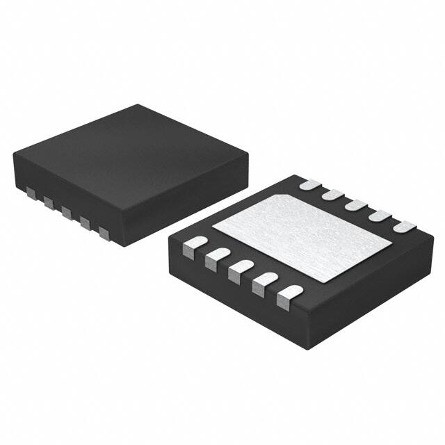
in the WDFN-10L 3x3 and WQFN-20L 5x5 packages.
RTQ2522A/B
Pin 1 Orientation***
(2) : Quadrant 2, Follow EIA-481-D
Package Type
QW : WDFN-10L 3x3 (W-Type)
QW : WQFN-20L 5x5 (W-Type)
Lead Plating System
G : Green (Halogen Free and Pb Free)
Applications
A : WDFN-10L 3x3
B : WQFN-20L 5x5
PCs, Servers, Modems, and Set-Top-Boxes
FPGA Applications
DSP Core and I/O Voltages
Instrumentation
Post-Regulation Applications
Applications With Sequencing Requirements
Note :
***Empty means Pin1 orientation is Quadrant 1
Richtek products are :
RoHS compliant and compatible with the current requirements of IPC/JEDEC J-STD-020.
Suitable for use in SnPb or Pb-free soldering processes.
Simplified Application Circuit
RTQ2522A/B
VIN
CIN
VBIAS
VIN
PGOOD
EN
VOUT
RPGOOD
VBIAS
CBIAS
Copyright © 2019 Richtek Technology Corporation. All rights reserved.
DSQ2522A/B-03 August 2019
VOUT
FB
SS
CSS
R1
COUT
R2
GND
is a registered trademark of Richtek Technology Corporation.
www.richtek.com
1
�RTQ2522A/B
Pin Configuration
VOUT
VOUT
VOUT
NC
FB
16
15
SS
14
NC
13
NC
4
12
GND
5
11
EN
VOUT
1
NC
2
NC
3
NC
VIN
GND
21
WDFN-10L 3x3
6
7
8
9
10
VBIAS
7
6
17
PGOOD
11
8
VOUT
VOUT
FB
SS
GND
18
VIN
4
5
10
9
19
VIN
1
2
3
20
VIN
VIN
VIN
PGOOD
VBIAS
EN
GND
(TOP VIEW)
WQFN-20L 5x5
Marking Information
RTQ2522BGQW
RTQ2522AGQW
KK= : Product Code
RTQ2522BGQW : Product Number
RTQ2522B
GQW
YMDNN
YMDNN : Date Code
KK=YM
DNN
YMDNN : Date Code
Functional Pin Description
Pin No.
WDFN-10L 3x3
WQFN-20L 5x5
1, 2
5, 6, 7, 8
9, 10
1, 18, 19, 20
Pin Name
Pin Function
VIN
Power input of the device.
VOUT
Regulated output voltage. A minimum of 2.2F capacitor
should be placed directly at this pin.
3
9
PGOOD
Power good indicator. An open-drain, active-high output that
indicates the status of VOUT. A pull-up resistor from 10k to
1M should be connected from this pin to a supply of up to
5.5V.
4
10
VBIAS
Bias input pin. Providing input voltage for internal control
circuitry.
5
11
EN
Chip enable (Active-High). Pulling this pin below 0.4V turns
the regulator off, reducing the quiescent current to a fraction
of its operating value. Connect to VIN if not being used.
6,
12,
GND
11 (Exposed Pad) 21 (Exposed Pad)
7
15
SS
Copyright © 2019 Richtek Technology Corporation. All rights reserved.
www.richtek.com
2
Ground. The Exposed Pad must be soldered to a large PCB
and connected to GND for maximum power dissipation.
Connect a capacitor between this pin and the ground to set
the soft-start ramp time of the output voltage.
is a registered trademark of Richtek Technology Corporation.
DSQ2522A/B-03 August 2019
�RTQ2522A/B
Pin No.
WDFN-10L 3x3
WQFN-20L 5x5
8
16
--
Pin Name
Pin Function
FB
Feedback pin. Connect this pin to an external voltage divider
to set the output voltage.
2, 3, 4, 13, 14, 17 NC
No internal connection. This pin can be left floating or
connected to GND.
Functional Block Diagram
Current
Limit
VIN
VOUT
UVLO
VBIAS
SS
+
+
Soft-Start
Discharge
Thermal
Protection
0.8V
Reference
FB
PGOOD
EN
Hysteresis
and Deglitch
0.9 x VREF
+
GND
Operation
The RTQ2522A/B is a very low dropout linear regulator
which operates from input voltage as low as 0.8V. It
provides a highly accurate output that is capable of
supplying 2A of output current with a typical dropout
voltage of only 135mV. Output voltage range is from 0.8V
to 3.6V.
VIN and VBIAS Supply
The VBIAS input supplies the internal reference and LDO
circuitry while all output current comes directly from the
VIN input for high efficiency regulation. With external VBIAS
3.25V above VOUT, offers the RTQ2522A/B very low
dropout performance (150mV Max. at 2A) which allows
the device to be used in place of a DC-DC converter
and still achieve good efficiency. This provides designers
to achieve the smallest, simplest, and lowest cost solution.
For applications where an auxiliary bias voltage is not
Copyright © 2019 Richtek Technology Corporation. All rights reserved.
DSQ2522A/B-03 August 2019
available or low dropout is not required. In these
applications, VBIAS is suggested be 1.8V above VOUT
and attention on power rating and thermal is needed.
Enable and Shutdown
The EN pin is active high. Apply a voltage above 1.1V
ensures the LDO regulator turns on, while the regulator
turns off if the VEN belows 0.4V. The enable circuitry has
typical 50mV hysteresis and deglitching for use with
relatively slowly ramping analog signals. That helps avoid
on-off cycling as a result of small glitches in the VEN signal.
A fast rise-time signal must be used to enable the
RTQ2522A/B if precise turn-on timing is required. If not
used, EN can be connected to either VIN or VBIAS. If EN
is connected to VIN, it should be connected as close as
possible to the largest capacitance on the input to prevent
voltage droops on that line from triggering the enable
circuit.
is a registered trademark of Richtek Technology Corporation.
www.richtek.com
3
�RTQ2522A/B
Soft-Start
The RTQ2522A/B includes a soft-start feature to prevent
excessive current flow during start-up. When the LDO is
enabled, an internal soft-start current (ISS) charges the
external soft-start capacitor (CSS) to build a ramp-up voltage
internally. The RTQ2522A/B achieve a linear and
monotonic soft-start by tracking the voltage ramp until
the voltage exceeds the internal reference. The soft-start
ramp time can be calculated using Equation 1 :
tSS (s) =
0.8V CSS (F)
VREF CSS
=
ISS
0.44 A
(1)
Power GOOD
When the output voltage is greater than VIT + VHYS, the
output voltage is considered good and the open-drain
PGOOD pin goes high impedance and is typically pulled
high with external resistor. If VOUT drops below VIT or if
VBIAS drops below 1.9 V, the open-drain output turns on
and pulls the PGOOD output low. The PGOOD pin also
asserts when the device is disabled, OCP or OTP
triggered.
Over-Current Protection
The RTQ2522A/B has built-in over-current protection.
When over current (typ. 3A) is detected, the RTQ2522A/
B foldback and limit the current at typical 2.25A. It allows
the device to supply surges of up to 3A and prevent the
device over-heating if short circuit happened.
Thermal Protection
At higher temperatures, or in cases where internal power
dissipation causes excessive self heating on chip, the
thermal shutdown circuitry will shut down the LDO when
the junction temperature exceeds approximately 160°C.
It will re enable the LDO once the junction temperature
drops back to approximately 140°C. The RTQ2522A/B will
cycle in and out of thermal shutdown without latch-up or
damage until the overstress condition is removed. Long
term overstress (TJ > 125°C) should be avoided as it can
degrade the performance or shorten the life of the part.
Copyright © 2019 Richtek Technology Corporation. All rights reserved.
www.richtek.com
4
is a registered trademark of Richtek Technology Corporation.
DSQ2522A/B-03 August 2019
�RTQ2522A/B
Absolute Maximum Ratings
(Note 1)
Supply Input Voltage, VIN ---------------------------------------------------------------------------------------- −0.3V to 6V
Other Pins ------------------------------------------------------------------------------------------------------------ −0.3V to 6V
Output Voltage, VOUT -------------------------------------------------------------------------------------------- −0.3V to (VIN + 0.3V)
Power Dissipation, PD @ TA = 25°C
WDFN-10L 3x3 ------------------------------------------------------------------------------------------------------ 3.27W
WQFN-20L 5x5 ----------------------------------------------------------------------------------------------------- 3.54W
Package Thermal Resistance (Note 2)
WDFN-10L 3x3, θJA ------------------------------------------------------------------------------------------------ 30.5°C/W
WDFN-10L 3x3, θJC ------------------------------------------------------------------------------------------------ 7.5°C/W
WQFN-20L 5x5, θJA ------------------------------------------------------------------------------------------------ 28.2°C/W
WQFN-20L 5x5, θJC ----------------------------------------------------------------------------------------------- 7.1°C/W
Junction Temperature ---------------------------------------------------------------------------------------------- 150°C
Lead Temperature (Soldering, 10 sec.) ------------------------------------------------------------------------ 260°C
Storage Temperature Range ------------------------------------------------------------------------------------- −65°C to 150°C
ESD Susceptibility (Note 3)
HBM (Human Body Model) --------------------------------------------------------------------------------------- 2kV
Recommended Operating Conditions
(Note 4)
Supply Input Voltage ----------------------------------------------------------------------------------------------- 0.8V to 5.5V
Ambient Temperature Range ------------------------------------------------------------------------------------- −40°C to 105°C
Electrical Characteristics
(VEN = 1.1V, VIN = VOUT + 0.3V, VBIAS = 5V, CBIAS = 0.1μF, CIN = COUT = 10μF, CSS = 1nF, IOUT = 50mA, TA = −40°C to 105°C, unless
otherwise specified. Typical values are at TA = 25°C)
Parameter
Symbol
Test Conditions
Min
Typ
Max
Unit
VOUT +
VDROP
--
5.5
V
2.7
--
5.5
V
Input Voltage
VIN
VBIAS Pin Voltage
VBIAS
Internal Reference
VREF
TA = 25C
0.796
0.8
0.804
V
Output Voltage Range
VOUT
VIN = 5V, IOUT = 2A
VREF
--
3.6
V
2.97V VBIAS 5.5V,
50mA IOUT 2A
2
0.5
2
%
--
%/V
Accuracy
Line Regulation
VLINE
VOUT (Normal) + 0.3 VIN 5.5V
--
0.03
Load Regulation
VLOAD
50mA IOUT = 2A
--
0.09
VIN Dropout Voltage
VDROP_VIN
IOUT = 2A,
VBIAS VOUT (Normal) 3.25V
--
100
150
mV
VBIAS Dropout Voltage
VDROP_VBIAS IOUT = 2A, VIN = VBIAS
--
1.55
1.8
V
Current Limit
ILIM
2.5
--
5.5
A
Copyright © 2019 Richtek Technology Corporation. All rights reserved.
DSQ2522A/B-03 August 2019
VOUT = 80% × VOUT (Normal)
%/A
is a registered trademark of Richtek Technology Corporation.
www.richtek.com
5
�RTQ2522A/B
Parameter
Bias Pin Current
Symbol
Test Conditions
Min
Typ
Max
Unit
--
1
2
mA
--
1
50
A
1
0.15
1
A
1kHz, IOUT = 1.5A,
VIN = 1.8V, VOUT = 1.5V
--
60
--
300kHz, IOUT = 1.5A,
VIN = 1.8V, VOUT = 1.5V
--
30
--
1kHz, IOUT = 1.5A,
VIN = 1.8V, VOUT = 1.5V
--
50
--
300kHz, IOUT = 1.5A,
VIN = 1.8V, VOUT = 1.5V
--
30
--
IBIAS
Shutdown Supply Current (IGND) ISHDN
Feedback Pin Current
VEN = 0.4V
IFB
Power-Supply Rejection
(VIN to VOUT)
PSRR
(Note 5)
Power-Supply Rejection
(VBIAS to VOUT)
dB
dB
Output Noise Voltage
Noise
(Note 5)
100Hz to 100kHz,
IOUT = 1.5A, CSS = 0.001F
--
25 x
VOUT
--
VRMS
Minimum Startup Time
tSTR
(Note 5)
RLOAD for IOUT = 1A,
CSS = open
--
200
--
s
Soft-Start Charging Current
ISS
VSS = 0.4V
--
440
--
nA
Logic_High
VIH
1.1
--
5.5
Logic_Low
VIL
0
--
0.4
Enable Pin Hysteresis
VEN_HYS
--
50
--
mV
Enable Pin Deglitch Time
VEN_DG
--
20
--
s
Enable Pin Current
IEN
VEN = 5V
--
0.1
1
A
PGOOD Trip Threshold
VIT
VOUT decreasing
85
90
94
%VOUT
PGOOD Trip Hysteresis
VHYS
--
3
--
%VOUT
PGOOD Output Low Voltage
VPGOOD_ L
IPGOOD = 1mA (sinking),
VOUT < VIT
--
--
0.3
V
PGOOD Leakage Current
IPGOOD_LK
VPGOOD = 5.25 V, VOUT > VIT
--
0.1
1
A
Shutdown, temperature
increasing
--
165
--
Reset, temperature decreasing
--
140
--
Enable Input
Voltage
Thermal Shutdown Temperature TSD
V
C
Note 1. Stresses beyond those listed under “Absolute Maximum Ratings” may cause permanent damage to the device.
These are stress ratings only, and functional operation of the device at these or any other conditions beyond those
indicated in the operational sections of the specifications is not implied. Exposure to absolute maximum rating
conditions may affect device reliability.
Note 2. θJA is measured under natural convection (still air) at TA = 25°C with the component mounted on a high effectivethermal-conductivity four-layer test board on a JEDEC 51-7 thermal measurement standard. θJC is measured at the
exposed pad of the package.
Note 3. Devices are ESD sensitive. Handling precaution is recommended.
Note 4. The device is not guaranteed to function outside its operating conditions.
Note 5. Guaranteed by design.
Copyright © 2019 Richtek Technology Corporation. All rights reserved.
www.richtek.com
6
is a registered trademark of Richtek Technology Corporation.
DSQ2522A/B-03 August 2019
�RTQ2522A/B
Typical Application Circuit
RTQ2522A
1, 2
VIN
CIN
VIN
5
EN
4
VBIAS
CBIAS
PGOOD
VOUT
VBIAS
FB
7 SS
CSS
3
9, 10
CFF
*Option
8
RPGOOD
VOUT
R1
COUT
R2
GND
6, 11 (Exposed Pad)
VIN
5, 6, 7, 8
CIN
11
10
VBIAS
CBIAS
RTQ2522B
VIN
PGOOD
EN
VOUT
9
1, 18, 19, 20
CFF
*Option
VBIAS
FB
15 SS
CSS
RPGOOD
VOUT
R1
COUT
16
R2
GND
12, 21 (Exposed Pad)
* : The feedforward capacitor is optional for the transient response and circuit stability improvement.
Table 1. Suggested Component Value
VOUT (V)
R1 (k)
R2 (k)
0.8
Short
Open
0.9
0.619
4.99
1.0
1.13
4.53
1.05
1.37
4.42
1.1
1.87
4.99
1.2
2.49
4.99
1.5
4.12
4.75
1.8
3.57
2.87
2.5
3.57
1.69
3.3
3.57
1.15
Copyright © 2019 Richtek Technology Corporation. All rights reserved.
DSQ2522A/B-03 August 2019
is a registered trademark of Richtek Technology Corporation.
www.richtek.com
7
�RTQ2522A/B
Typical Operating Characteristics
Enable Voltage Threshold vs. Temperature
VBIAS Voltage UVLO vs. Temperature
0.90
2.29
Enable Voltage Threshold (V)1
2.31
Logic_High
VBIAS Voltage (V)
2.27
2.25
2.23
2.21
2.19
2.17
logic_Low
2.15
2.13
VIN = 1.8V, VOUT = 1.2V, VBIAS = 5V, IOUT = 50mA
2.11
0.85
Logic_High
0.80
0.75
logic_Low
0.70
0.65
0.60
0.55
VIN = 1.8V, VOUT = 1.2V, VBIAS = 5V, IOUT = 50mA
0.50
-50
-25
0
25
50
75
100
125
-50
-25
0
Reference Voltage vs. Temperature
(VIN - VOUT) Dropout Voltage (mV)
Reference Voltage (V)
0.805
0.800
0.795
VIN = 1.8V, no load
0.790
0
25
50
75
100
105°C
25°C
−40°C
100
80
60
40
20
VIN = 1.5V, VBIAS = 5V
0
0
500
250
105°C
25°C
−40°C
100
50
VIN = 1.5V, IOUT = 2A
0
2
2.5
3
3.5
4
4.5
VBIAS - VOUT (V)
Copyright © 2019 Richtek Technology Corporation. All rights reserved.
www.richtek.com
8
5
Output Spectral Noise Density (μV /Hz)1
VIN - VOUT (mV)
300
1.5
1000
1500
2000
Output Current (mA)
VIN Dropout Voltage vs. (VBIAS - VOUT)
1
125
120
125
350
150
100
140
Temperature (°C)
200
75
Dropout Voltage vs. Output Current
0.810
-25
50
Temperature (°C)
Temperature (°C)
-50
25
Output Spectral Noise Density
100
10
1
0.1
0.01
VIN = 1.5V, VOUT = 1.2V, COUT = 10μF, ILOAD = 1.5A
0.001
10
100
1000
10000
100000
Frequency (Hz)
is a registered trademark of Richtek Technology Corporation.
DSQ2522A/B-03 August 2019
�RTQ2522A/B
VBIAS PSRR vs. Frequency
100
80
90
70
80
70
60
PSRR (dB)
PSRR (dB)
VIN PSRR vs. Frequency
90
50
40
ILOAD = 0.1A
ILOAD = 1.5A
30
60
50
ILOAD = 0.1A
ILOAD = 0.5A
ILOAD = 1.5A
40
30
20
20
10
VIN = 1.8V, VOUT = 1.2V, COUT = 10μF, CSS = 1nF
VIN = 1.8V, VOUT = 1.2V, VBIAS = 5V,
COUT = 10μF, CSS = 1nF
10
0
0
10
100
1K
10K
100K
1M
10
10M
100
1K
10K
100K
1M
Frequency (Hz)
Frequency (Hz)
Power Up Response
Load Transient Response
10M
CSS = 0nF
CSS = 2.2nF
VOUT
(500mV/Div)
VOUT
(50mV/Div)
CSS = 1nF
IOUT
(1A/Div)
EN
(2V/Div)
VIN = 2.5V, VOUT = 1.5V, IOUT = 100mA to 1.5A
Time (1ms/Div)
Copyright © 2019 Richtek Technology Corporation. All rights reserved.
DSQ2522A/B-03 August 2019
Time (50μs/Div)
is a registered trademark of Richtek Technology Corporation.
www.richtek.com
9
�RTQ2522A/B
Application Information
The RTQ2522A/B is a low dropout regulator that features
soft-start capability. It provides EN and PGOOD for easily
system sequence control, and built-in over current &
thermal protection for safe operation.
Dropout Voltage
Power Up Sequence Requirement
The RTQ2522A/B supports power on the input VIN,
VBIAS, and EN pins in any order without damage the
device. Generally, connecting the EN and VIN for most
application is acceptable, as long as VIN and VEN is greater
The second, VBIAS dropout voltage is the voltage
difference (VBIAS − VOUT) when VIN and VBIAS pins are
joined together and VOUT starts to decrease. This option
allows the device to be used in applications where an
auxiliary bias voltage is not available or low dropout is not
required. In these applications, VBIAS is suggested be
1.8V above VOUT and attention on power rating and
thermal is needed.
than the EN threshold (typ. = 1.1V) and the input ramp
rate of VIN and VBIAS is faster than the output settled
soft-start ramp rate. If the VIN/BIAS input source ramp
rate is slower than the output settled soft-start time, the
output will track the input supply ramp up level and minus
the dropout voltage until it reaches the settled output voltage
level. For the other case, If EN is connected with VBIAS,
and the provided VIN is present before VBIAS, the output
soft-start will as programmed. While VBIAS and VEN are
present before VIN is applied also the settled soft-start
time has expired, then VOUT tracks VIN ramp up. If the
soft-start time has not expired, output tracks VIN ramp up
until output reaches the value set by the charging softstart capacitor.
Input, Output, and Bias Capacitor Selection
Thermal Considerations
The device is designed to be stable for all available types
and values of output capacitors ≥ 2.2μF. The device is
also stable with multiple capacitors in parallel, which can
be of any type or value. The capacitance required on the
VIN and VBIAS pins strongly depends on the input supply
source impedance. To counteract any inductance in the
input, the minimum recommended capacitor for VIN is 1μF
and minimum recommended capacitor for VBIAS is 0.1μF.
If VIN and VBIAS are connected to the same supply, the
recommended minimum capacitor for VBIAS is 4.7μF. Good
quality, low ESR capacitors should be used on the input;
ceramic X5R and X7R capacitors are preferred. These
capacitors should be placed as close the pins as possible
for optimum performance.
The junction temperature should never exceed the
absolute maximum junction temperature TJ(MAX), listed
under Absolute Maximum Ratings, to avoid permanent
damage to the device. The maximum allowable power
dissipation depends on the thermal resistance of the IC
package, the PCB layout, the rate of surrounding airflow,
and the difference between the junction and ambient
temperatures. The maximum power dissipation can be
calculated using the following formula :
Because of two power supply inputs VIN and VBIAS and
one VOUT regulator output, there are two Dropout voltages
specified. The first is the VIN Dropout voltage is the voltage
difference (VIN − VOUT) when VOUT starts to decrease
by percent specified in the Electrical Characteristics table.
Adjusting the Output Voltage
The output voltage of the RTQ2522A/B is adjustable from
0.8V to 3.6V by external voltage divider resisters as shown
in Typical Application Circuit. R1 and R2 can be calculated
the output voltage. In order to achieve the maximum
accuracy specifications, R2 should be ≤ 4.99kΩ.
Copyright © 2019 Richtek Technology Corporation. All rights reserved.
www.richtek.com
10
PD(MAX) = (TJ(MAX) − TA) / θJA
where TJ(MAX) is the maximum junction temperature, TA is
the ambient temperature, and θJA is the junction-to-ambient
thermal resistance.
For continuous operation, the maximum operating junction
temperature indicated under Recommended Operating
Conditions is 125°C. The junction-to-ambient thermal
resistance, θJA, is highly package dependent. For a
WDFN-10L 3x3 package, the thermal resistance, θJA, is
30.5°C/W on a standard JEDEC 51-7 high effective-thermalconductivity four-layer test board. For a WQFN-20L 5x5
is a registered trademark of Richtek Technology Corporation.
DSQ2522A/B-03 August 2019
�RTQ2522A/B
package, the thermal resistance, θJA, is 28.2°C/W on a
standard JEDEC 51-7 high effective-thermal-conductivity
four-layer test board. The maximum power dissipation at
TA = 25°C can be calculated as below :
PD(MAX) = (125°C − 25°C) / (30.5°C/W) = 3.27W for a
WDFN-10L 3x3 package.
PD(MAX) = (125°C − 25°C) / (28.2°C/W) = 3.54W for a
WQFN-20L 5x5 package.
The maximum power dissipation depends on the operating
ambient temperature for the fixed TJ(MAX) and the thermal
resistance, θJA. The derating curves in Figure 1 allows
the designer to see the effect of rising ambient temperature
on the maximum power dissipation.
Maximum Power Dissipation (W)1
4.0
WQFN-20L 5x5
Layout Considerations
For best performance of the RTQ2522A/B, the PCB layout
suggestions below are highly recommend :
Input capacitor must be placed as close as possible to
IC to minimize the power loop area.
Minimize the power trace length and avoid using vias for
the input and output capacitors connection.
Figure 2 and Figure 3 shows the examples for the layout
reference which helps the inductive parasitic components
minimization, load transient reduction and good circuit
stability.
Four-Layer PCB
3.5
3.0
WDFN-10L 3x3
2.5
2.0
1.5
1.0
0.5
0.0
0
25
50
75
100
125
Ambient Temperature (°C)
Figure 1. Derating Curve of Maximum Power Dissipation
Copyright © 2019 Richtek Technology Corporation. All rights reserved.
DSQ2522A/B-03 August 2019
is a registered trademark of Richtek Technology Corporation.
www.richtek.com
11
�RTQ2522A/B
GND layout trace should be
wider for thermal consideration.
GND Plane
VOUT Plane
VIN Plane
PGOOD reference
source input
COUT
CIN
VIN
VIN
PGOOD
VBIAS
EN
CBIAS
Enable signal
input
10
9
1
2
3
4
5
8
7
6
11
VOUT
VOUT
FB
SS
GND
CSS
R1
R2
GND Plane
Add via for thermal consideration
Figure 2. RTQ2522A PCB Layout Guide
GND Plane
VOUT
VIN Plane
5
4
3
2
VIN
NC
NC
NC
CIN
VOUT Plane
1
VIN
6
20
VOUT
VIN
7
19
VOUT
VIN
8
18
VOUT
PGOOD
9
17
NC
VBIAS
10
16
FB
Enable signal input
13
14
R1
COUT
R2
15
SS
12
NC
11
NC
GND
EN
CBIAS
21
GND
PGOOD reference
source input
CSS
GND Plane
Add via for thermal consideration
Figure 3. RTQ2522B PCB Layout Guide
Copyright © 2019 Richtek Technology Corporation. All rights reserved.
www.richtek.com
12
is a registered trademark of Richtek Technology Corporation.
DSQ2522A/B-03 August 2019
�RTQ2522A/B
Outline Dimension
D2
D
L
E
E2
1
e
SEE DETAIL A
b
2
1
2
1
A
A1
A3
DETAIL A
Pin #1 ID and Tie Bar Mark Options
Note : The configuration of the Pin #1 identifier is optional,
but must be located within the zone indicated.
Symbol
Dimensions In Millimeters
Dimensions In Inches
Min
Max
Min
Max
A
0.700
0.800
0.028
0.031
A1
0.000
0.050
0.000
0.002
A3
0.175
0.250
0.007
0.010
b
0.180
0.300
0.007
0.012
D
2.950
3.050
0.116
0.120
D2
2.300
2.650
0.091
0.104
E
2.950
3.050
0.116
0.120
E2
1.500
1.750
0.059
0.069
e
L
0.500
0.350
0.020
0.450
0.014
0.018
W-Type 10L DFN 3x3 Package
Copyright © 2019 Richtek Technology Corporation. All rights reserved.
DSQ2522A/B-03 August 2019
is a registered trademark of Richtek Technology Corporation.
www.richtek.com
13
�RTQ2522A/B
1
1
2
2
DETAIL A
Pin #1 ID and Tie Bar Mark Options
Note : The configuration of the Pin #1 identifier is optional,
but must be located within the zone indicated.
Symbol
Dimensions In Millimeters
Dimensions In Inches
Min.
Max.
Min.
Max.
A
0.700
0.800
0.028
0.031
A1
0.000
0.050
0.000
0.002
A3
0.175
0.250
0.007
0.010
b
0.250
0.350
0.010
0.014
D
4.900
5.100
0.193
0.201
D2
3.100
3.200
0.122
0.126
E
4.900
5.100
0.193
0.201
E2
3.100
3.200
0.122
0.126
0.650
e
L
0.500
0.026
0.600
0.020
0.024
W-Type 20L QFN 5x5 Package
Copyright © 2019 Richtek Technology Corporation. All rights reserved.
www.richtek.com
14
is a registered trademark of Richtek Technology Corporation.
DSQ2522A/B-03 August 2019
�RTQ2522A/B
Footprint Information
Footprint Dimension (mm)
Package
Number of
Pin
P
A
B
C
D
Sx
Sy
M
V/W/U/X/ZDFN3*3-10
10
0.50
3.80
2.10
0.85
0.30
2.55
1.70
2.30
Copyright © 2019 Richtek Technology Corporation. All rights reserved.
DSQ2522A/B-03 August 2019
Tolerance
±0.05
is a registered trademark of Richtek Technology Corporation.
www.richtek.com
15
�RTQ2522A/B
Footprint Dimension (mm)
Package
Number of
Pin
P
Ax
Ay
Bx
By
C
D
Sx
Sy
V/W/U/XQFN5*5-20
20
0.65
5.80
5.80
3.80
3.80
1.00
0.40
3.25
3.25
Tolerance
±0.05
Richtek Technology Corporation
14F, No. 8, Tai Yuen 1st Street, Chupei City
Hsinchu, Taiwan, R.O.C.
Tel: (8863)5526789
Richtek products are sold by description only. Customers should obtain the latest relevant information and data sheets before placing orders and should verify
that such information is current and complete. Richtek cannot assume responsibility for use of any circuitry other than circuitry entirely embodied in a Richtek
product. Information furnished by Richtek is believed to be accurate and reliable. However, no responsibility is assumed by Richtek or its subsidiaries for its use;
nor for any infringements of patents or other rights of third parties which may result from its use. No license is granted by implication or otherwise under any patent
or patent rights of Richtek or its subsidiaries.
www.richtek.com
16
DSQ2522A/B-03 August 2019
�


 工商网监
湘ICP备2023018690号
工商网监
湘ICP备2023018690号
