R1130x SERIES
300mA LDO REGULATOR
NO.EA-078-140822
OUTLINE
The R1130x Series are CMOS-based voltage regulator (VR) ICs. VR function has features of high ripple
rejection, low dropout voltage, high output voltage accuracy, and ultra-low supply current. Each of these ICs
consists of a voltage reference unit, an error amplifier, resistors for setting output voltage, and a current limit
circuit. Each of the R1130xxxxA/B type includes also a chip enable circuit.
The output voltage of the R1130xxxxC type is adjustable with external resistors.
The output voltage of R1130xxxxA/B is fixed in the IC. Low supply current by the merit of CMOS process and
built-in transistors with low ON-resistance make low dropout voltage. These regulators in the R1130x Series are
remarkable improvement on the current regulators in terms of ripple rejection, input transient response, and load
transient response. Maximum Output Current is large for its compact size.
Thus, the R1130x Series are suitable for power supply for CD-drives, DVD-drives, and so forth.
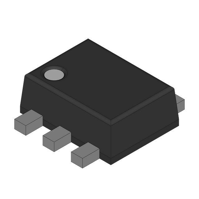
Since the packages for these ICs are the SOT-89-5 package or HSON-6 (Discontinued), high density mounting
of the ICs on boards is possible.
FEATURES
•
•
•
•
•
•
•
•
•
•
•
•
Supply Current .......................................................... Typ. 50µA
Standby Current ........................................................ Typ. 0.1µA (VR) for A type
Ripple Rejection ........................................................ Typ. 60dB (f=1kHz) (VR)
Output Current .......................................................... Min. 300mA (VIN=VOUT+1V)
Output Voltage Range............................................... 1.5V to 5.0V (0.1V steps)
Externally specified with the ADJUST pin
(Reference Voltage 1.8V : C Version)
(For other voltages, please refer to MARK INFORMATIONS.)
Output Voltage Accuracy........................................... ±2.0%(VR) for A/B type,
±2.0% (Reference Voltage for adjustable VR) for C type
Dropout Voltage ........................................................ Typ. 0.2V (IOUT=100mA) (VR)
Temperature-drift Coefficient of Output Voltage ...... ±100ppm/°C
Absolute Maximum Voltage ..................................... 9.0V
Packages ................................................................. SOT-89-5, HSON-6 (Discontinued)
Built-in Current Limit Circuit
Internal Phase Compensation (small output capacitance such as 0.1µF Ceramic can be used with.)
APPLICATIONS
• Power source for CD-drives and DVD-drives, HDD.
• Local Power source for Notebook PC.
1
�R1130x
BLOCK DIAGRAMS
2
R1130HxxxA
R1130DxxxA (Discontinued)
R1130HxxxB
R1130DxxxB (Discontinued)
R1130HxxxC
R1130DxxxC (Discontinued)
�R1130x
SELECTION GUIDE
The output voltage, CE pin polarity, package for the ICs can be selected at the user’s request.
Product Name
Package
Quantity per Reel
Pb Free
Halogen Free
R1130Dxx1∗-TR-FE
HSON-6 (Discontinued)
3,000 pcs
Yes
Yes
R1130Hxx1∗-T1-FE
SOT-89-5
1,000 pcs
Yes
Yes
xx : The output voltage can be designated in the range from 1.5V(15) to 5.0V(50) in 0.1V steps.
(C Version is fixed at 00.)
(For other voltages, please refer to MARK INFORMATIONS.)
∗ : CE pin polarity are options as follows.
(A) "L" active
(B) "H" active
(C) "H" active, with ADJUST pin.
3
�R1130x
PIN CONFIGURATION
• SOT-89-5
5
• HSON-6
Top View
4
6
5
Bottom View
4
4
5
6
∗
∗
1
2
3
1
2
3
∗
3
2
1
PIN DESCRIPTIONS
•
SOT-89-5
Pin No.
Symbol
1
VOUT
Voltage Regulator Output Pin
2
VDD
Input Pin
3
GND
4
5
•
Description
Ground Pin
NC (A/B type)
No Connection
ADJ (C type)
Adjustable Regulator feedback Input Pin
(Connect to resistor voltage divider.)
CE (A type)or
CE(B/D type)
Chip Enable Pin
HSON-6 (Discontinued)
Pin No.
Symbol
1
VDD
2
GND
3
Description
Input Pin
Ground Pin
NC (A/B type)
No Connection
ADJ (C type)
Adjustable Regulator feedback Input Pin
(Connect to resistor voltage divider.)
4
NC
No Connection
5
CE (A type)or
CE(B/D type)
Chip Enable Pin
6
VOUT
Voltage Regulator Output Pin
∗) Tab and tab suspension leads are VDD level. (They are connected to the reverse side of the IC.)
The tab is better to be connected to the VDD, but leaving it open is also acceptable.
The tab suspension leads should be open and do not connect to other wires or land patterns.
4
�R1130x
ABSOLUTE MAXIMUM RATINGS
Symbol
Item
Rating
Unit
9.0
V
VIN
Input Voltage
VCE
Input Voltage
( CE or CE Input Pin)
−0.3~9.0
V
VADJ
Input Voltage (ADJ Input Pin)
−0.3~9.0
V
VOUT
Output Voltage
−0.3~VIN+0.3
V
IOUT
Output Current
450
mA
Power Dissipation (SOT-89-5)*
900
Power Dissipation (HSON-6)* (Discontinued)
900
PD
mW
Topt
Operating Temperature Range
−40~85
°C
Tstg
Storage Temperature Range
−55~125
°C
∗) For Power Dissipation, please refer to PACKAGE INFORMATION.
ABSOLUTE MAXIMUM RATINGS
Electronic and mechanical stress momentarily exceeded absolute maximum ratings may cause the
permanent damages and may degrade the life time and safety for both device and system using the device
in the field.
The functional operation at or over these absolute maximum ratings is not assured.
RECOMMENDED OPERATING CONDITIONS (ELECTRICAL CHARACTERISTICS)
All of electronic equipment should be designed that the mounted semiconductor devices operate within the
recommended operating conditions. The semiconductor devices cannot operate normally over the
recommended operating conditions, even if when they are used over such conditions by momentary
electronic noise or surge. And the semiconductor devices may receive serious damage when they continue
to operate over the recommended operating conditions.
5
�R1130x
ELECTRICAL CHARACTERISTICS
•
R1130xxxxA
Topt=25°C
Symbol
Conditions
Min.
Typ.
2.5
Max.
Unit
8.0
V
VIN
Input Voltage
ISS1
Supply Current 1
VIN-VOUT=1.0V,VIN=GND
50
100
µA
Istandby
Standby Current
VIN-VOUT=1.0V,VIN=VCE
0.1
1.0
µA
VOUT
Output Voltage
VIN-VOUT=1.0V
1mA <
= IOUT <
= 80mA
Set
VOUT
VOUT×
1.020
V
IOUT1
Output Current
Refer to the table of Input
Voltage by Set Output Voltage
VIN-VOUT=1.0V
1mA <
= IOUT <
= 80mA
VOUT×
0.980
300
mA
∆VOUT/∆IOUT
Load Regulation
VDIF
Dropout Voltage
IOUT=100mA
∆VOUT/∆VIN
Line Regulation
IOUT=80mA,Set VOUT>2.0V:
VOUT+0.5V <
= 8.0V
= VIN <
Set OUT <
= VIN <
= 1.9V: .5V <
= 8.0V
0.1
Ripple Rejection
f=1kHz Ripple 0.5Vp−p
IOUT = 80mA
Set VOUT >
= 1.8V, VIN−VOUT = 1.0V
Set VOUT <
= 1.7, VIN = 2.8V
60
dB
Output Voltage
Temperature Coefficient
IOUT = 30mA, VIN−VOUT = 1.0V
−40°C <
= Topt <
= 85°C
±100
ppm
/°C
RR
∆VOUT/
∆Topt
6
Item
Set VOUT
ISC
Short Current Limit
RPU
CE Pull-up Resistance
VCEH
CE Input Voltage “H”
VIN=2.5V
VCEL
CE Input Voltage “L”
VIN=2.5V
<
=
40
80
mV
Refer to the ELECTRICAL
CHARACTERISTICS by
OUTPUT VOLTAGE
3.9V,VOUT = 0V
0.2
70
Set VOUT>4.0V,VOUT = 0V
mA
50
2.5
5.0
%/V
10.0
MΩ
1.5
VIN
V
0.00
0.25
V
�R1130x
•
R1130xxxxB
Topt=25°C
Symbol
Item
Conditions
Min.
Typ.
VIN
Input Voltage
2.5
ISS1
Supply Current 1
VIN-VOUT=1.0V, VIN=VCE
50
Istandby
Standby Current
VIN-VOUT=1.0V, VIN=GND
0.1
VOUT
Output Voltage
VIN-VOUT=1.0V
1mA <
= IOUT <
= 80mA
IOUT1
Output Current
VOUT×
0.980
Refer to the table of Input
Voltage by Set Output Voltage
VIN-VOUT=1.0V
1mA <
= IOUT <
= 80mA
∆VOUT/∆IOUT
Load Regulation
VDIF
Dropout Voltage
IOUT=100mA
Line Regulation
IOUT=80mA,
Set VOUT>2.0V: VOUT+0.5V
<
= 8.0V
Set VOUT <
= 1.9V:
<
2.5V <
V
IN
=
= 8.0V
Ripple Rejection
f=1kHz Ripple 0.5Vp−p
IOUT = 80mA
Set VOUT >
= 1.8V, VIN−VOUT = 1.0V
Set VOUT <
= 1.7, VIN = 2.8V
Output Voltage
Temperature Coefficient
IOUT = 10mA, VIN−VOUT = 1.0V
−40°C <
= Topt <
= 85°C
∆VOUT/∆VIN
RR
∆VOUT/
∆Topt
Set
VOUT
40
<
=
0.1
CE Input Voltage “L”
VIN=2.5V
V
80
mV
2.5
0.2
%/V
ppm
/°C
50
VCEL
VOUT×
1.020
±100
4.0V,VOUT = 0V
VIN=2.5V
µA
dB
>
=
CE Input Voltage “H”
µA
60
Set VOUT
VCEH
100
VIN
70
Pull-down Resistance
for CE pin
V
Refer to the Table of Dropout
Voltage by Set Output Voltage
3.9V,VOUT = 0V
RPU
8.0
mA
<
=
Short Current Limit
Unit
300
Set VOUT
ISC
Max.
5.0
mA
10.0
MΩ
1.5
VIN
V
0.00
0.25
V
7
�R1130x
•
Dropout Voltage by Set Output Voltage
Dropout Voltage by Set Output Voltage
Topt = 25°C
Dropout Voltage
Output Voltage
VOUT (V)
•
Topt = 25°C
Output Voltage
VOUT (V)
VDIF (V)
Input Voltage
(V)
Typ.
Max.
1.5
<
=
VOUT
<
=
1.9
VIN=VOUT+1.5V
VOUT = 1.5
1.00
1.05
2.0
<
=
VOUT
<
=
2.7
VIN=VOUT+1.3V
VOUT = 1.6
0.90
0.95
2.8
<
=
VOUT
<
=
5.0
VIN=VOUT+1.0V
VOUT = 1.7
0.80
0.85
VOUT = 1.8
0.70
0.75
VOUT = 1.9
0.60
0.65
VOUT = 2.0
0.50
0.60
VOUT = 2.1
0.40
0.55
2.2
<
=
VOUT
<
=
2.5
0.30
0.49
2.6
<
=
VOUT
<
=
3.3
0.25
0.34
3.4
<
=
VOUT
<
=
5.0
0.20
0.28
R1130xxxxC
Topt=25°C
Symbol
Conditions
Min.
Typ.
Unit
8.0
V
Input Voltage
ISS1
Supply Current
VIN-VOUT=1.0V, VIN=VCE
50
100
µA
Standby Current
VIN-VOUT=1.0V, VIN=GND
0.1
1.0
µA
VOUT
Reference Voltage for
Adjustable Voltage
Regulator
VOUT=VADJ,VIN-VOUT=1.0V
IOUT=80mA
1.764
1.800
1.836
V
IOUT1
Output Current
VOUT=VADJ, VIN-VOUT=1.5V
300
∆VOUT/∆IOUT
Load Regulation
VIN=2.5V, VOUT=VADJ
1mA <
= IOUT <
= 80mA
40
80
mV
VDIF
Dropout Voltage
IOUT=100mA, VOUT=VADJ
0.1
0.2
V
∆VOUT/∆VIN
Line Regulation
IOUT=80mA, VOUT=VADJ
2.5V <
= VIN <
= 8.0V
0.1
0.2
%/V
RR
Ripple Rejection
f=1kHz Ripple 0.5Vp−p
IOUT = 80mA,VIN−VOUT = 1.0V
VOUT=VADJ,IOUT=80mA
60
dB
Output Voltage
Temperature Coefficient
IOUT = 10mA, VIN−VOUT = 1.0V
−40°C <
= Topt <
= 85°C
±100
ppm
/°C
ISC
Short Current Limit
VOUT = 0V
70
mA
RPU
Pull-down Resistance
for CE pin
VCEH
CE Input Voltage “H”
VIN=2.5V
VCEL
CE Input Voltage “L”
VIN=2.5V
∆VOUT/
∆Topt
2.5
Max.
VIN
Istandby
8
Item
2.5
mA
5.0
10.0
MΩ
1.5
VIN
V
0.00
0.25
V
�R1130x
TEST CIRCUITS (Pin number is applied to R1130H Series)
•
R1130HxxxA
Fig.1 Standard test Circuit
Fig.2 Supply Current Test Circuit
Fig.3 Ripple Rejection, Line Transient
Response Test Circuit
Fig.4 Load Transient Response Test Circuit
9
�R1130x
•
10
R1130HxxxB
Fig.1 Standard test Circuit
Fig.2 Supply Current Test Circuit
Fig.3 Test Circuit for Ripple Rejection and
Input Transient Response
Fig.4 Test Circuit for Load Transient Response
�R1130x
•
R1130H001C
Fig.1 Standard test Circuit
Fig.2 Test Circuit Supply Current
Fig.3 Test Circuit for Ripple Rejection and
Input Transient Response
Fig.4 Test Circuit for Load Transient Response
11
�R1130x
TYPICAL CHARACTERISTICS
1) Output Voltage vs. Output Current (Topt=25°C)
R1130x151B
R1130x331B
R1130x501B
2) Input Voltage vs. Output Voltage (Topt=25°C)
R1130x151B
12
R1130x331B
�R1130x
R1130x501B
3) Dropout Voltage vs. Output Current
R1130x151B
R1130x331B
R1130x501B
13
�R1130x
4) Output Voltage vs. Temperature
R1130x151B
R1130x331B
R1130x501B
5) Supply Current vs. Input Voltage (Topt=25°C)
R1130x151B
14
R1130x331B
�R1130x
R1130x501B
6) Supply Current vs. Temperature
R1130x151B
R1130x331B
R1130x501B
15
�R1130x
7) Ripple Rejection vs. Frequency
R1130x151B
R1130x331B
R1130x501B
8) Ripple Rejection vs. Input Voltage
R1130x151B
16
R1130x331B
�R1130x
R1130x501B
9) Input Transient Response
R1130x151B
R1130x151B
17
�R1130x
R1130x501B
10) Load Transient Response
R1130x151B
R1130x331B
18
�R1130x
R1130x501B
19
�R1130x
APPENDIX
* Technical Notes on Output Voltage Setting of C type
Figure 1. Adjustable Regulator (C type)
The Output Voltage of Regulator in R1130xxxxC may be adjustable for any output voltage between its 1.8V
reference and its VDD setting level. An external pair of resistors is required, as shown in Figure 1.
The complete equation for the output voltage is described step by step as follows;
I2=IIC+I3 ································································································· (1)
I3=1.8/R3 ······························································································· (2)
Thus,
I2=IIC+1.8/R3
··························································································· (3)
Therefore,
VOUT=1.8+R2×I2 ·····················································································
Put Equation (3) into Equation (4), then
VOUT=1.8+R2×(IIC+1.8/R3)
=1.8×(1+R2/R3)+R2×IIC ····································································
In 2nd term, or R2×IIC will produce an error in VOUT.
In Equation (5),
IIC=1.8/RIC ·······························································································
R2×IIC=R2×1.8/RIC
=1.8×R2/RIC ··················································································
For better accuracy, choosing R2 (