R1155x Series
150 mA 24 V Input High Voltage Regulator
NO.EA-270-150702
OUTLINE
The R1155x is a CMOS-based 24 V input voltage regulator featuring 150 mA output that provides high output
voltage accuracy and low supply current. Internally, the R1155x consists of a voltage reference unit, an error
amplifier, and a resistor net for setting output voltage. As protection circuits, the R1155x contains a current limit
circuit, a fold-back protection circuit, a thermal shutdown circuit and a reverse current protection circuit.
The R1155x is available in the fixed output voltage type (R1155xxxxB), and the adjustable output voltage type
(R1155x001C). The output voltage accuracy for the fixed output voltage type is as high as ±2.0%.
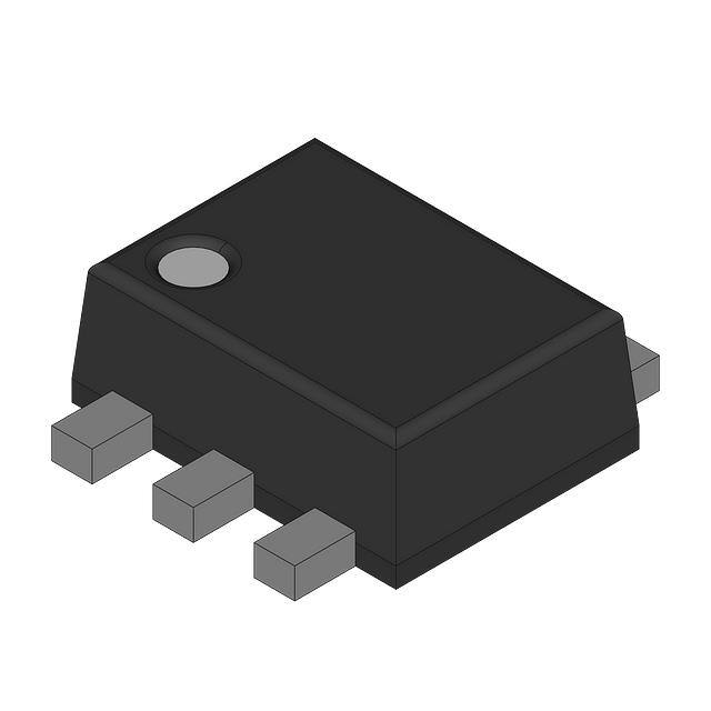
The R1155x is offered in a 5-pin SOT-89-5 package and a 5-pin SOT-23-5 package.
FEATURES
Supply Current ········································· Typ. 7.5 µA (VIN = 6.0 V or 3.0 V)
Standby Current ········································ Typ. 0.1 µA
Output Current ·········································· Min. 150 mA (VIN = 6.0 V or 3.0 V)
Output Voltage Accuracy ····························· ±2.0%
Package ·················································· SOT-23-5, SOT-89-5
Input Voltage Range ·································· Max. 24.0 V
Output Voltage Range ································ Fixed Output Voltage Type: 2.5 V to 12.0 V
Adjustable Output Voltage Type: 2.5 V, 2.5 V to 23.0 V
using external resistor
Fold-back Protection Circuit ························· Typ. 30 mA
Thermal Shutdown Circuit
Reverse Current Protection Circuit
Ceramic Capacitor Capable ························· COUT = 4.7 µF or more
APPLICATIONS
Power source for home appliances (refrigerators, rice cookers, electric water warmers, etc.)
Power source for in-car audio systems, in-car navigation systems, ETC systems, and reset circuits
Power source for laptop personal computers, digital TVs, cordless phones, and private LAN systems for
home, and reset circuits
Power source for copiers, printers, facsimiles, scanners, and reset circuits
1
�R1155x
NO.EA-270-150702
SELECTION GUIDE
The output voltage, the output voltage type, and the package type for the ICs are user-selectable options.
Selection Guide
Product Name
Package
Quantity per Reel
Pb Free
Halogen Free
R1155Nxxx-TR-FE
SOT-23-5
3,000 pcs
Yes
Yes
R1155Hxxx-T1-FE
SOT-89-5
1,000 pcs
Yes
Yes
xxx: Designation of the output voltage (VSET)
For Fixed Output Voltage Type: 2.5 V (025) to 12 V (120) in 0.1 V steps
For Adjustable Output Voltage Type: 2.5 V (001) only
: Designation of the output voltage type
(B) Fixed Output Voltage Type
(C) Adjustable Output Voltage Type
BLOCK DIAGRAMS
Reverse Current
Protection
Reverse Current
Protection
VDD
VOUT
VDD
VOUT
Voltage
Reference
Voltage
Reference
VFB
On/Off
Control
On/Off
Control
Thermal
Shutdown
Current
Limit
VCE
2
GND
VCE
Thermal
Shutdown
Current
Limit
R1155xxxxB Block Diagram
R1155x001C Block Diagram
(Fixed Output Voltage Type)
(Adjustable Output Voltage Type)
GND
�R1155x
NO.EA-270-150702
PIN DESCRIPTION
5
4
5
4
(mark side)
1
2
3
1
SOT-23-5 Pin Configuration
2
3
SOT-89-5 Pin Configuration
SOT-23-5 Pin Description
Pin No
Symbol
1
VOUT
VR Output Pin
2
GND
Ground Pin
3
VDD
Input Pin
TP1
R1155NxxxB
Test Pin
VFB2
R1155N001C3
VR Adjustment Pin
4
5
CE
Description
Chip Enable Pin, Active-high
SOT-89-5 Pin Description
Pin No
Symbol
1
VOUT
VR Output Pin
2
GND
Ground Pin
3
CE
Chip Enable Pin, Active-high
TP1
R1155HxxxB
Test Pin
VFB2
R1155H001C3
VR Adjustment Pin
VDD
Input Pin
4
5
Description
1
The TP pin must be connected to GND.
A 24 MΩ or less voltage setting resistor must be connected to the VFB pin.
3
As for the adjustable output voltage type (R1155N001C), please refer to ADJUSTABLE OUTPUT VOLTAGE TYPE
SETTING.
2
3
�R1155x
NO.EA-270-150702
PIN EQIVALENT CIRCUIT DIAGRAMS
Driver
CE
VOUT
VOUT Pin Equivalent Circuit Diagram
VFB Pin Equivalent Circuit Diagram
VOUT
TP
TP Pin Equivalent Circuit Diagram
(R1155xxxxB)
4
VOUT
VFB
VFB Pin Equivalent Circuit Diagram
(R1155x001C)
�R1155x
NO.EA-270-150702
ABSOLUTE MAXIMUM RATINGS
Absolute Maximum Ratings
Symbol
Item
Rating
Unit
−0.3 to 26
V
−0.3 to VIN +0.3
V
VIN
Input Voltage
VCE
Input Voltage (CE Pin)
VOUT
Output Voltage
−0.3 to 26
V
VVFB
Output Voltage (VFB Pin)
−0.3 to 26
V
IOUT
Output Current
350
mA
PD
Power Dissipation (Standard Land Pattern)1
Tj
Junction Temperature
−40 to 125
C
Storage Temperature Range
−55 to 125
C
Tstg
SOT-23-5
420
SOT-89-5
900
mW
ABSOLUTE MAXIMUM RATINGS
Electronic and mechanical stress momentarily exceeded absolute maximum ratings may cause the permanent
damages and may degrade the life time and safety for both device and system using the device in the field. The
functional operation at or over these absolute maximum ratings is not assured.
RECOMMENDED OPERATING CONDITIONS
Recommended Operating Ratings
Symbol
Item
Ta
Operating Temperature Range
VIN
Input Voltage
Ratings
Unit
−40 to 105
°C
3.5 to 24
V
RECOMMENDED OPERATING RATINGS
All of electronic equipment should be designed that the mounted semiconductor devices operate within the
recommended operating ratings. The semiconductor devices cannot operate normally over the recommended
operating ratings, even if when they are used over such ratings by momentary electronic noise or surge. And the
semiconductor devices may receive serious damage when they continue to operate over the recommended
operating ratings.
1
Refer to POWER DISSIPATION in SUPPLEMENTSRY ITEMS for detail information.
5
�R1155x
NO.EA-270-150702
ELECTRICAL CHARACTERISTICS
VIN = VCE = VSET + 3.0 V, COUT = 4.7 μF, IOUT = 1 mA, unless otherwise noted.
The specifications surrounded by
are guaranteed by Design Engineering at −40°C ≤ Ta ≤ 105°C.
R1155xxxxB, R1155x001C Electrical Characteristics
Symbol
ILIM
VOUT
ISS1
ISS2
Item
Conditions
Output Current
VIN = VSET + 4 V
Output Voltage
(Low Power Mode)
IOUT = 1 mA
Supply Current
(Low Power Mode)
Supply Current (Fast Mode)
Istandby Standby Current
(Ta = 25C)
mA
x0.98
x1.02
V
−40°C ≤ Ta ≤ 105°C x0.955
x1.03
V
22
A
4.2 < VSET ≤ 8.4 V
8.6
22
A
8.4 < VSET ≤ 12 V
9.5
22
A
IOUT = 10 mA
65
125
A
VIN = 24 V, VCE = 0 V
0.1
1.0
A
0
1.5
%
2.5 ≤ VSET ≤ 5 V
30
90
mV
5 < VSET ≤ 12 V
30
100
mV
IOUT = 0 mA
∆VOUT
/∆IOUT
Load Regulation (Fast Mode)
6 mA ≤ IOUT ≤ 150 mA
-1.5
Line Regulation (Low Power Mode)
VSET + 0.2 V ≤ VIN ≤ 24 V
IOUT = 1 mA
0.3
1.3
%
Line Regulation (Fast Mode)
VSET + 0.2 V ≤ VIN ≤ 24 V
IOUT = 10 mA
1.2
2.4
%
2.5V ≤ VSET < 3.3 V
1.6
2.6
V
3.3 V ≤ VSET < 5 V
0.96
2.1
V
5 ≤ VSET ≤ 12 V
0.55
1.7
V
2.5 ≤ VSET < 5 V
60
dB
5 ≤ VSET ≤ 12 V
50
dB
±100
ppm
/°C
Dropout Voltage
Ripple Rejection (Fast Mode)
IOUT = 150 mA
f = 1 kHz, 0.5 Vp-p,
IOUT = 10 mA
∆VOUT
/∆Ta
Output Voltage
Temperature Coefficient
IOUT = 1 mA, −40°C ≤ Ta ≤ 105°C
IOUTH
Fast Mode Switching Current
IOUT = Light Load → Heavy Load
IOUTL
Low Power Mode Switching Current
IOUT =
Short Current Limit
VOUT = 0 V
ISC
Unit
7.5
1 mA ≤ IOUT ≤ 6 mA
RR
Max.
2.5 ≤ VSET ≤ 4.2 V
Output Voltage Deviation
When Switching Mode
VDIF
Typ.
150
Ta = 25ºC
∆VOUT
∆VOUT
/∆VIN
Min.
Heavy Load → Light Load
2.4
4.5
6.5
mA
0.6
1.5
2.4
mA
30
mA
VCEH
CE Input Voltage “H”
1.35
VIN
V
VCEL
CE Input Voltage “L”
0
0.5
V
TTSD
Thermal Shutdown Temperature
Junction Temperature
145
°C
TTSR
Thermal Shutdown
Released Temperature
Junction Temperature
120
°C
All test items listed under ELECTRICAL CHARACTERISTICS are done under the pulse load condition (Tj ≈Ta = 25°C) except
for Ripple Rejection and Output Voltage Temperature Coefficient.
6
�R1155x
NO.EA-270-150702
ELECTRICAL CHARACTERISTICS (continued)
VIN = VCE = VSET + 3.0 V, COUT = 4.7 μF, IOUT = 1 mA, unless otherwise noted.
The specifications surrounded by
are guaranteed by Design Engineering at −40°C ≤ Ta ≤ 105°C.
R1155xxxxB, R1155x001C Electrical Characteristics
Symbol
IREV
Item
Reverse Current Limit
(Ta = 25C)
Conditions
CE = GND,
VIN = VSET + 0.02 V
Typ.
Max.
Unit
2.5 ≤ VSET < 5 V
1.0
3.5
A
5 ≤ VSET ≤ 12 V
2.0
6.0
A
Reverse Current Protection
VREV_DET Mode Detection Offset1
VREV = VDD - VOUT
0 ≤ VIN ≤ 24.0 V, VOUT ≥ 2.0 V
Reverse Current Protection
Mode Release Offset1
0 ≤ VIN ≤ 24.0 V, VOUT ≥ 2.0 V
VREV_REL
Min.
20
mV
220
mV
All test items listed under ELECTRICAL CHARACTERISTICS are done under the pulse load condition (Tj ≈Ta = 25°C) except
for Ripple Rejection and Output Voltage Temperature Coefficient.
The operation of reverse current protection circuit is guaranteed when VOUT ≥ 2.0 V. The reverse current protection
mode is always turned on when VIN = 0 V.
1
7
�R1155x
NO.EA-270-150702
THEORY OF OPERATION
Power Activation
When starting up the IC using the input voltages of the VDD and CE pins simultaneously with no load, the both
pin voltages have to be 0.06 V/ ms or faster. When starting up the IC using the both pin voltages at 0.06 V/ ms
or slower with no load, the VDD pin has to be started up before the CE pin.
Thermal Shutdown Circuit
The R1155x contains a thermal shutdown circuit, which stops regulator operation if the junction temperature
of the R1155x becomes higher than 145°C (Typ.). Additionally, if the junction temperature after the regulator
being stopped decreases to a level below 120°C (Typ.), it restarts regulator operation. As a result the operation
of the thermal shutdown circuit causes the regulator repeatedly to turn off and on until the causes of
overheating are removed. As a consequence a pulse shaped output voltage occurs.
Reverse Current Protection Circuit
The R1155x includes a reverse current protection circuit, which stops the reverse current flowing from the
VOUT to VDD pins or to GND pin when VOUT becomes more than VIN.
Usually, the LDO using Pch output transistor contains a parasitic diode between VDD pin and VOUT pin.
Therefore, if VOUT is more than VIN, the parasitic diode becomes forward direction. As a result, the current flows
from VOUT pin to VDD pin.
The R1155x switches the mode to the reverse current protection mode before VIN becomes smaller than VOUT
by connecting the parasitic diode of Pch output transistor to the backward direction, and connecting the gate
to VOUT pin. As a result, the Pch output transistor is turned off and the all the current pathways from VOUT
pin to GND pin are shut down to maintain the reverse current lower than [IREV] of the Electrical Characteristics.
Switching to either the normal mode or to the reverse current protection mode is determined by the magnitude
of VIN voltage and VOUT voltage. For the stable operation, offset and hysteresis are set as the threshold. The
detection/ release thresholds of both normal and reverse current protection modes are specified by [VREV_DET]
and [VREV_REL] of the Electrical Characteristics. Therefore, the minimum dropout voltage under the small load
current condition is restricted by the value of [VREV_REL].
Figure 7 and Figure 8 show the normal operation mode and reverse current protection mode, respectively.
Figure 9 shows the detection/ release timing of reverse current protection function. When giving the VOUT pin
a constant-voltage and decreasing the VIN voltage, the dropout voltage will become lower than the [VREV_DET].
As a result, the reverse current protection starts to function to stop the load current. By increasing the dropout
voltage more than the [VREV_REL], the protection mode will be released to let the load current to flow. If the
dropout voltage to be used is smaller than [VREV_REL], the detection and the release may be repeated.
The operation coverage of the reverse current protection circuit is VOUT ≥ 1.5 V. However, under the condition
of VIN = 0 V, always the reverse current protection mode is operating.
8
�R1155x
NO.EA-270-150702
Reverse
Detector
VIN
Reverse
Detector
VIN
IOUT
IREV
-
-
+
+
VOUT
Vref
Vref
GND
GND
Output/ Reverse Current
IOUT/ IREV
Input/ Output Voltage
VIN/ VOUT [V]
Normal Operation Mode
VOUT
Reverse Current Protection Mode
VIN
VREV_REL
VREV_DET
VOUT
IOUT
Normal Mode
Reverse Current Protection Mode
Normal
Mode
0
IREV
Detection/ Release Timing of Reverse Current Protection Function
9
�R1155x
NO.EA-270-150702
APPLICATION INFORMATION
V IN
V IN
V DD
R1155xxxxB
CIN
V OUT
V OUT
CE
GND
CIN
COUT
V DD
R115 5x00 1C
V OUT
CE
GND
V OUT
R1
V FB
COUT
R2
R1155xxxxB Typical Application
R1155x001C Typical Application
(Fixed Output Voltage Type)
(Adjustable Output Voltage Type)
Technical Notes on the Components Selection
In the R1155x, phase compensation is provided to secure stable operation even when the load current is
varied. For this purpose, use a 4.7 μF or more output capacitor (COUT) with good frequency
characteristics and proper ESR (Equivalent Series Resistance). In case of using a tantalum type
capacitor and the ESR value of the capacitor is large, the output might be unstable. Evaluate the circuit
including consideration of frequency characteristics.
Ensure the VDD and GND lines are sufficiently robust. If their impedance is too high, noise pickup or
unstable operation may result. Connect COUT with suitable values between the VOUT and GND pins, and
as close as possible to the pins. Please refer to Figure 5 and Figure 6 below.
10
�R1155x
NO.EA-270-150702
Adjustable Output Voltage Type Setting (R1155x001C)
The output voltage of the R1155x001C can be adjusted up to 23 V by using the external divider resistors (R1,
R2). The resistance value for R2 should be set to 24 MΩ or less. By using the following equations, the output
voltage can be determined. VFB voltage which is fixed inside the IC is described as setVFB. setVFB is 2.5 V.
When using the R1155x001C with 2.5 V, please connect the VOUT pin to the VFB pin.
VOUT
R1
I1
VFB
R IC
R2
GND
VOUT
IIC
I2
setVFB
Output Voltage Adjustment Using External Divider Resistors
I1 = IIC + I2.......................................................................................................................................(1)
I2 = setVFB / R2................................................................................................................................(2)
Thus,
I1 = IIC + setVFB / R2 ......................................................................................................................... (3)
Therefore,
VOUT = setVFB + R1 x I1.................................................................................................................... (4)
Insert Equation (3) into Equation (4), so
VOUT = setVFB + R1 x (IIC + setVFB / R2)
= setVFB x (1+ R1 / R2) + R1 x IIC ............................................................................................ (5)
In Equation (5), R1xIIC is the error-causing factor in VOUT.
As for IIC,
IIC = setVFB / RIC…………………………………………………………………………………………………………………………………………………(6)
Therefore, the error-causing factor R1x IIC can be described as follows.
R1 x IIC = R1 x setVFB / RIC
= setVFB R1 / RIC .............................................................................................................. (7)
For better accuracy, choosing R1 (