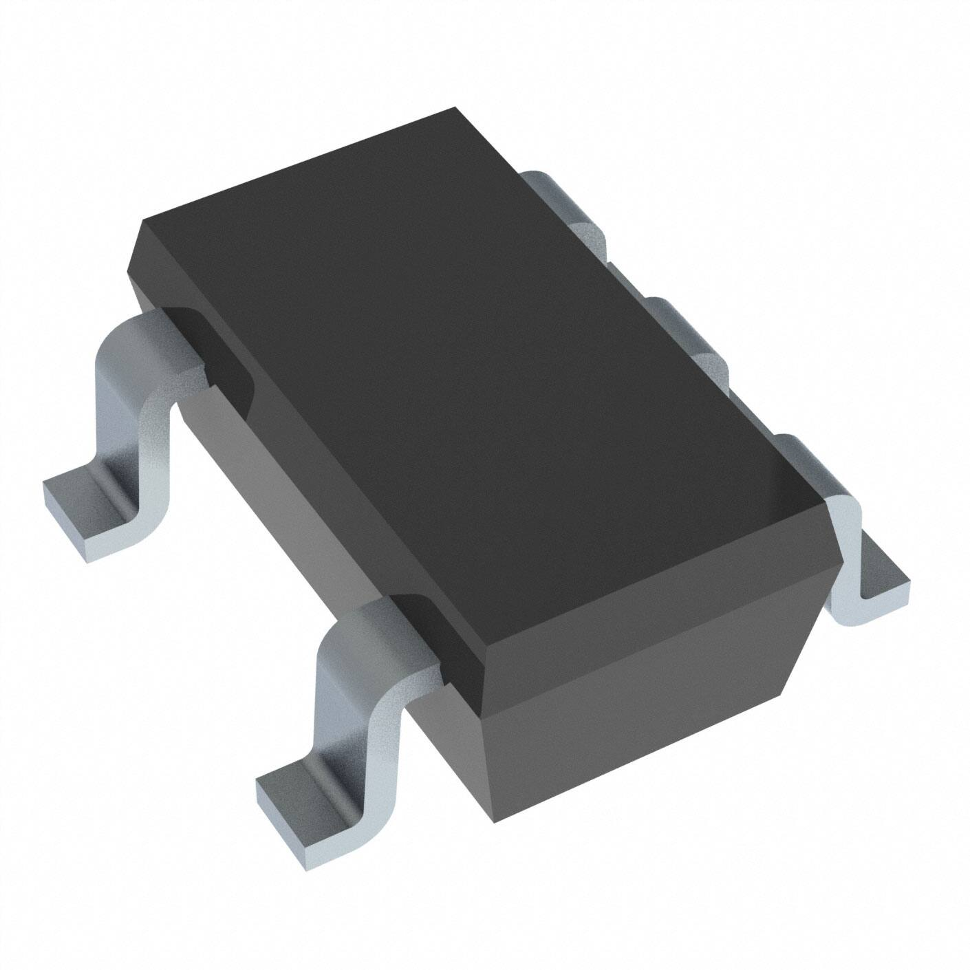
R1163K (DFN(PLP)1616-6) is the non-promotional product as of March 2019.
R1163x SERIES
3-MODE 150mA LDO REGULATOR with the Reverse Current Protection
NO.EA-118-190320
OUTLINE
The R1163x Series consist of CMOS-based voltage regulator ICs with high output voltage accuracy and low
supply current. These ICs perform with the chip enable function and realize a standby mode with ultra low supply
current. To prevent the destruction by over current, the current limit circuit is included. The R1163x Series have
3-mode. One is standby mode with CE or standby control pin. Other two modes are realized with ECO pin. Fast
Transient Mode (FT mode) and Low Power Mode (LP mode) are alternative with ECO pin. Consumption current
is reduced at Low Power Mode compared with Fast Transient Mode. The output voltage is maintained between
FT mode and LP mode.
Further, the reverse current protection circuit is built-in. Therefore, if a higher voltage than VDD pin is forced to
the output pin, the reverse current to VDD pin is very small (Max. 0.1A) , so it is suitable for backup circuit.
Since the packages for these ICs are SOT-23-5, SON-6, and DFN(PLP)1616-6 packages, high density
mounting of the ICs on boards is possible.
FEATURES
Supply Current ..................................................... Typ. 6.0A (Low Power Mode),
Typ. 70A (Fast Transient Mode)
Standby Mode ...................................................... Typ. 0.6A
Reverse Current ................................................... Max. 0.1A
Input Voltage Range ............................................ 2.0V to 6.0V
Output Voltage Range .......................................... 1.5V to 5.0V (0.1V steps)
(For other voltages, please refer to MARK INFORMATIONS.)
Output Voltage Accuracy...................................... 1.5% (2.5% at Low Power Mode)
Temperature-Drift Coefficient of Output Voltage .. Typ. 100ppm/C
Dropout Voltage ................................................... Typ. 0.25V (IOUT150mA, VOUT2.8V)
Ripple Rejection ................................................... Typ. 70dB (f1kHz, Fast Transient Mode)
Line Regulation .................................................... Typ. 0.02%/V (Fast Transient Mode)
Packages ............................................................ DFN(PLP)1616-6, SOT-23-5, SON-6
Built-in fold-back protection circuit ....................... Typ. 40mA (Current at short mode)
Performs with Ceramic Capacitors ...................... CINCeramic 1.0F, COUTCeramic 0.47F
APPLICATIONS
Precision Voltage References.
Power source for electrical appliances such as cameras, VCRs and hand-held communication equipment.
Power source for battery-powered equipment.
1
�R1163K (DFN(PLP)1616-6) is the non-promotional product as of March 2019.
R1163x
BLOCK DIAGRAM
R1163xxx1B
R1163xxx1D
ECO
VDD
ECO
VOUT
VDD
VOUT
Vref
Vref
Current Limit
Current Limit
Reverse Detector
CE
GND
R1163xxx1E
ECO
VDD
VOUT
Vref
Current Limit
CE
2
Reverse Detector
GND
CE
Reverse
Detector
GND
�R1163K (DFN(PLP)1616-6) is the non-promotional product as of March 2019.
R1163x
SELECTION GUIDE
The output voltage, auto discharge function, and package, etc. for the ICs can be selected at the user’s
request.
Product Name
Package
Quantity per Reel
Pb Free
Halogen Free
DFN(PLP)1616-6
5,000 pcs
Yes
Yes
R1163Nxx1-TR-FE
SOT-23-5
3,000 pcs
Yes
Yes
R1163Dxx1-TR-FE
SON-6
3,000 pcs
Yes
Yes
R1163Kxx1-TR
xx : The output voltage can be designated in the range from 1.5V(15) to 5.0V(50) in 0.1V steps.
(For other voltages, please refer to MARK INFORMATIONS.)
: The auto discharge function at off state are options as follows.
(B) without auto discharge function at off state
(D) with auto discharge function at off state
(E) without auto discharge function at off state, ECO logic reverse type (Low Power mode at ECO"H")
3
�R1163K (DFN(PLP)1616-6) is the non-promotional product as of March 2019.
R1163x
PIN CONFIGURATIONS
DFN(PLP)1616-6
Top View
6
5
SOT-23-5
Bottom View
4
4
5
SON-6
Top View
5
4
6
6
5
Bottom View
4
4
5
1
2
3
(mark side)
3
2
1
1
2
3
1
2
3
3
PIN DISCRIPTIONS
DFN(PLP)1616-6
Pin No
1
2
3
4
5
6
Symbol
VOUT
GND
ECO
ECO
CE
NC
VDD
Pin Description
Output pin
Ground Pin
R1163xxx1B/D: FT/LP Mode Alternative Pin (“L” LP)
R1163xxx1E: FT/LP Mode Alternative Pin (“H” LP)
Chip Enable pin ("H" Active)
No Connection
Input Pin
) Tab is GND level. (They are connected to the reverse side of this IC.)
The tab is better to be connected to the GND, but leaving it open is also acceptable.
SOT-23-5
Pin No
1
2
3
4
5
Symbol
VDD
GND
CE
ECO
ECO
VOUT
Pin Description
Input Pin
Ground Pin
Chip Enable Pin ("H" Active)
R1163xxx1B/D: FT/LP Mode Alternative Pin (“L” LP)
R1163xxx1E: FT/LP Mode Alternative Pin (“H” LP)
Output pin
SON-6
Pin No
1
2
3
4
5
6
Symbol
VDD
NC
VOUT
ECO
ECO
GND
CE
Pin Description
Input Pin
No Connection
Output pin
R1163xxx1B/D: FT/LP Mode Alternative Pin (“L” LP)
R1163xxx1E: FT/LP Mode Alternative Pin (“H” LP)
Ground Pin
Chip Enable Pin ("H" Active)
*) Tab suspension leads are GND level. (They are connected to the reverse side of this IC.)
The tab suspension leads should be open and do not connect to other wires or land patterns.
4
6
2
1
�R1163K (DFN(PLP)1616-6) is the non-promotional product as of March 2019.
R1163x
ABSOLUTE MAXIMUM RATINGS
Symbol
VIN
Item
Input Voltage
Rating
Unit
6.5
V
VECO
Input Voltage (ECO/ECO Pin)
0.3 ~ 6.5
V
VCE
Input Voltage (CE Pin)
0.3 ~ 6.5
V
VOUT
Output Voltage
0.3 ~ 6.5
V
IOUT
Output Current
180
mA
Power Dissipation (DFN(PLP)1616-6)*
640
Power Dissipation (SOT-23-5) *
420
Power Dissipation (SON-6) *
500
PD
mW
Topt
Operating Temperature Range
40 ~ 85
C
Tstg
Storage Temperature Range
55 ~ 125
C
) For Power Dissipation, please refer to PACKAGE INFORMATION.
ABSOLUTE MAXIMUM RATINGS
Electronic and mechanical stress momentarily exceeded absolute maximum ratings may cause the
permanent damages and may degrade the life time and safety for both device and system using the device
in the field.
The functional operation at or over these absolute maximum ratings is not assured.
RECOMMENDED OPERATING CONDITIONS (ELECTRICAL CHARACTERISTICS)
All of electronic equipment should be designed that the mounted semiconductor devices operate within the
recommended operating conditions. The semiconductor devices cannot operate normally over the
recommended operating conditions, even if when they are used over such conditions by momentary
electronic noise or surge. And the semiconductor devices may receive serious damage when they continue
to operate over the recommended operating conditions.
5
�R1163K (DFN(PLP)1616-6) is the non-promotional product as of March 2019.
R1163x
ELECTRICAL CHARACTERISTICS
Topt25C
R1163xxx1B/D
Symbol
Item
Conditions
FT Mode
VOUT
Output Voltage
LP Mode
VOUT
IOUT
VOUT/
Load Regulation
IOUT
FT Mode
LP Mode
VDIF
Dropout Voltage
ISS1
Supply Current (FT Mode)
ISS2
Supply Current (LP Mode)
Istandby Supply Current (Standby)
FT Mode
VOUT/
Line Regulation
VIN
LP Mode
RR
VIN
VOUT/
Topt
ISC
IPD
RPDE
VCEH
VCEL
en
RLOW
IREV
6
VINSet VOUT1V, VECOVIN
1mA
IOUT
30mA
VINSet VOUT 1V, VECOGND
1mA
IOUT
30mA
Output Voltage Deviation
VINSet VOUT1V,
between FT Mode and LP Mode IOUT30mA
Output Current
Ripple Rejection (FT Mode)
Input Voltage
Output Voltage
Temperature Coefficient
Short Current Limit
CE Pull-down Current
ECO Pull-down Resistance
CE, ECO Input Voltage "H"
CE, ECO Input Voltage "L"
Output Noise "H" (FT Mode)
Output Noise "L" (LP Mode)
Low Output Nch Tr.
ON Resistance (of D version)
Reverse Current
Min.
Typ.
0.985
1.015
0.975
1.025
VOUT > 2.0V
1.2
0
1.2
2.0V
24
150
0
24
VOUT
IOUT30mA, VECOVIN
If VOUT
1.7V, then
VINSet VOUT1.2V
Unit
V
VINVOUT1.0V
VINSet VOUT1V, VECOVIN
20
IOUT
150mA
1mA
VINSet VOUT1V, VECOGND
20
1mA
IOUT
150mA
Refer to the following table
VINSet VOUT1V
70
VECOVIN
VINSet VOUT1V
6.0
VECOGND
VINSet VOUT1V, VCEGND
0.6
VECOGND or VIN
Set VOUT0.5V
VIN
6.0V
IOUT30mA, VECOVIN
0.02
If VOUT
1.6V,
then 2.2V
VIN
6.0V
VIN
6.0V
Set VOUT 0.5V
IOUT 30mA, VECOGND
0.05
If VOUT
1.6V,
then 2.2V
VIN
6.0V
Ripple 0.2Vp-p,
70
f1kHz
VINSet VOUT1V,
%
mV
mA
40
mV
45
100
A
10.0
A
1.0
A
0.10
%/V
0.20
dB
60
f10kHz
2.0
IOUT30mA
40C
Topt
VOUT0V
Max.
6.0
100
85C
2
1.0
0
40
0.3
5
0.6
30
6.0
0.35
V
ppm
/C
mA
A
M
V
V
BW10Hz to 100kHz
BW10Hz to 100kHz
30
40
Vrms
VCE0V
60
VOUT>0.5V, 0V
VIN
6V
0
0.1
A
�R1163K (DFN(PLP)1616-6) is the non-promotional product as of March 2019.
R1163x
Topt25C
R1163xxx1E
Symbol
Item
Conditions
FT Mode
VOUT
Output Voltage
LP Mode
VOUT
IOUT
Output Voltage Deviation
VINSet VOUT1V, VOUT > 2.0V
between FT Mode and LP Mode IOUT30mA
2.0V
VOUT
Output Current
FT Mode
VOUT/
IOUT
Load Regulation
VDIF
Dropout Voltage
ISS1
Supply Current (FT Mode)
ISS2
Supply Current (LP Mode)
LP Mode
Istandby Supply Current (Standby)
FT Mode
VOUT/
VIN
Line Regulation
LP Mode
RR
VIN
VOUT/
Topt
ISC
IPD
VINSet VOUT1V, VECOGND
1mA
IOUT
30mA
VINSet VOUT 1V, VECOVIN
1mA
IOUT
30mA
Ripple Rejection (FT Mode)
Typ.
Max.
0.985
1.015
0.975
1.025
Unit
V
1.2
0
1.2
%
24
150
0
24
mV
VINVOUT1.0V
VINSet VOUT1V, VECOGND
20
1mA
IOUT
150mA
VINSet VOUT1V, VECOVIN
20
IOUT
150mA
1mA
Refer to the following table
VINSet VOUT1V
70
VECOGND
VINSet VOUT1V
6.0
VECOVIN
VINSet VOUT1V, VCEGND
0.6
VECOGND or VIN
VIN
6.0V
Set VOUT0.5V
IOUT30mA, VECOGND
0.02
1.6V,
If VOUT
then 2.2V
VIN
6.0V
Set VOUT 0.5V
VIN
6.0V
IOUT30mA, VECOVIN
0.05
If VOUT
1.6V,
then 2.2V
VIN
6.0V
Ripple 0.2Vp-p
70
f 1kHz
VINSet VOUT1V,
IOUT30mA,
VECOGND
If VOUT
60
1.7V, then f 10kHz
VINSet VOUT1.2V
2.0
IOUT 30mA
100
Topt
85C
40C
40
VOUT 0V
0.3
mA
40
mV
45
100
A
10.0
A
1.0
A
0.10
%/V
0.20
dB
VCEH
CE, ECO Input Voltage "H"
1.0
6.0
V
ppm
/C
mA
A
V
VCEL
CE, ECO Input Voltage "L"
Output Noise "H" (FT Mode)
Output Noise "L" (LP Mode)
Reverse Current
0
0.4
V
en
IREV
Input Voltage
Output Voltage
Temperature Coefficient
Short Current Limit
CE Pull-down Current
Min.
BW 10Hz to 100kHz
BW 10Hz to 100kHz
VOUT>0.5V, 0V
VIN
6V
30
40
0
6.0
0.6
Vrms
0.1
A
7
�R1163K (DFN(PLP)1616-6) is the non-promotional product as of March 2019.
R1163x
ELECTRICAL CHARACTERISTICS by OUTPUT VOLTAGE
Topt25C
Output Voltage
VOUT (V)
Dropout Voltage (mV)
VDIF (FT Mode)
Condition
Typ.
400
380
350
340
290
250
VOUT <
1.5
1.6
1.6
V
OUT
<
1.7
1.7 VOUT < 1.8
1.8
VOUT < 2.0
2.0
VOUT < 2.8
VOUT
5.0
2.8
IOUT150mA
VDIF (LP Mode)
Max.
680
550
520
490
425
350
Typ.
420
390
370
350
300
250
Max.
680
550
520
490
430
350
TYPICAL APPLICATION
VDD
C1
R1163x
Series
ECO
CE
VOUT
VOUT
C2
GND
External Components)
Ex. C1: Ceramic Capacitor 1.0F
C2: Ceramic Capacitor 0.47F
Murata GRM40B474K
Kyocera CM105B474K
TECHNICAL NOTES
When using these ICs, consider the following points:
Phase Compensation
In these ICs, phase compensation is made for securing stable operation even if the load current is varied. For
this purpose, be sure to use a 0.47F or more ceramic capacitor C2.
(Test these ICs with as same external components as ones to be used on the PCB.)
When a tantalum capacitor is used with this IC, if the equivalent series resistor (ESR) of the capacitor is large,
output voltage may be unstable.
PCB Layout
Make VDD and GND lines sufficient. If their impedance is high, noise pickup or unstable operation may result.
Connect a capacitor C1 with as much as 1.0F capacitor between VDD and GND pin as close as possible.
Set external components such as an output capacitor C2, as close as possible to the ICs and make wiring as
short as possible.
8
�R1163K (DFN(PLP)1616-6) is the non-promotional product as of March 2019.
R1163x
TEST CIRCUITS
VDD
C1
VOUT
VOUT
C2
V
R1163x
Series
GND
CE
IOUT
ECO
C1=Ceramic 1.0F
C2=Ceramic 0.47F
Basic Test Circuit
VDD
ISS
A
C1
VOUT
VOUT
C2
R1163x
Series
GND
CE
ECO
C1=Ceramic 1.0F
C2=Ceramic 0.47F
Test Circuit for Supply Current
Pulse
Generator
P.G.
VDD
VOUT
C2
IOUT
R1163x
Series
GND
CE
ECO
C1=Ceramic 1.0F
C2=Ceramic 0.47F
Test Circuit for Ripple Rejection, Line Transient Response
9
�R1163K (DFN(PLP)1616-6) is the non-promotional product as of March 2019.
R1163x
VDD
VOUT
VOUT
C2
R1163x
Series
GND
C1
CE
IOUT a IOUT b
V
ECO
C1=Ceramic 1.0F
C2=Ceramic 0.47F
Test Circuit for Load Transient Response
VDD
VOUT
R1163x
Series
GND
C1
CE
ECO
IOUT
C2
Pulse
Generator
P.G.
C1=Ceramic 1.0F
C2=Ceramic 0.47F
Test Circuit for Output Voltage at Mode alternative point
VDD
VOUT
C2
IOUT
R1163x
Series
GND
C1
CE
ECO
CE pin Input Waveform
P.G.
Set VOUT+1.0V
Pulse
Generator
0V
C1=Ceramic 1.0F
C2=Ceramic 0.47F
Test Circuit for Turn On Speed with CE pin
10
�R1163K (DFN(PLP)1616-6) is the non-promotional product as of March 2019.
R1163x
TYPICAL CHARACTERISTICS
Unless otherwise provided, capacitors are ceramic type.
1) Output Voltage vs. Output Current
R1163x151x FT Mode
R1163x151x LP Mode
1.6
1.4
Output Voltage L VOUTL(V)
Output Voltage H VOUTH(V)
1.6
VIN=2V
1.2
1.0
0.8
VIN=2.5V • 3.5V
0.6
0.4
0.2
0.0
0
100
200
300
Output Current IOUT(mA)
1.4
1.0
0.8
VIN=2.5V • 3.5V
0.6
0.4
0.2
0.0
400
VIN=2V
1.2
0
R1163x281x FT Mode
Output Voltage L VOUTL(V)
Output Voltage H VOUTH(V)
3.0
2.5
VIN=3.1V
2.0
VIN=3.3V
1.5
VIN=3.8V • 4.8V
1.0
0.5
0
100
200
300
Output Current IOUT(mA)
2.5
VIN=3.3V
1.5
VIN=3.8V • 4.8V
1.0
0.5
0.0
400
VIN=3.1V
2.0
0
4.5
4.5
4.0
4.0
VIN=4.3V
3.5
3.0
VIN=4.5V
2.5
VIN=5V • 6V
2.0
1.5
1.0
0.5
0
100
200
300
Output Current IOUT(mA)
100
200
300
Output Current IOUT(mA)
400
R1163x40x LP Mode
400
Output Voltage L VOUTL(V)
Output Voltage H VOUTH(V)
R1163x40x FT Mode
0.0
400
R1163x281x LP Mode
3.0
0.0
100
200
300
Output Current IOUT(mA)
VIN=4.5V
VIN=4.3V
3.5
VIN=5V • 6V
3.0
2.5
2.0
1.5
1.0
0.5
0.0
0
100
200
300
Output Current IOUT(mA)
400
11
�R1163K (DFN(PLP)1616-6) is the non-promotional product as of March 2019.
R1163x
2) Output Voltage vs. Input Voltage
R1163x15x LP Mode
1.6
1.4
1.4
Output Voltage L VOUTL(V)
Output Voltage H VOUTH(V)
R1163x151x FT Mode
1.6
1.2
1.0
0.8
0.6
0.4
IOUT=1mA
IOUT=30mA
IOUT=50mA
0.2
0.0
0
1
2
3
4
Input Voltage VIN(V)
5
1.2
1.0
0.8
0.6
0.4
0.2
0.0
6
IOUT=1mA
IOUT=30mA
IOUT=50mA
0
R1163x28x FT Mode
Output Voltage L VOUTL(V)
Output Voltage H VOUTH(V)
2.0
1.5
1.0
IOUT=1mA
IOUT=30mA
IOUT=50mA
0.5
0
1
2
3
4
Input Voltage VIN(V)
5
2.0
1.5
1.0
IOUT=1mA
IOUT=30mA
IOUT=50mA
0.5
0.0
6
0
4.5
4.0
4.0
3.5
3.0
2.5
2.0
1.5
IOUT=1mA
IOUT=30mA
IOUT=50mA
1.0
0.5
0
1
2
3
4
Input Voltage VIN(V)
1
2
3
4
Input Voltage VIN(V)
5
6
R1163x40x LP Mode
4.5
Output Voltage L VOUTL(V)
Output Voltage H VOUTH(V)
6
2.5
R1163x40x FT Mode
12
5
3.0
2.5
0.0
2
3
4
Input Voltage VIN(V)
R1163x28x LP Mode
3.0
0.0
1
5
6
3.5
3.0
2.5
2.0
1.5
IOUT=1mA
IOUT=30mA
IOUT=50mA
1.0
0.5
0.0
0
1
2
3
4
Input Voltage VIN(V)
5
6
�R1163K (DFN(PLP)1616-6) is the non-promotional product as of March 2019.
R1163x
3) Supply Current vs. Input Voltage
R1163x151x LP Mode
8
70
7
Supply Current ISS(μA)
Supply Current H ISSH(μA)
R1163x151x FT Mode
80
60
50
40
30
20
10
0
0
1
2
3
4
Input Voltage VIN(V)
5
6
5
4
3
2
1
0
6
0
8
70
7
60
50
40
30
20
10
0
0
1
2
3
4
Input Voltage VIN(V)
5
5
6
2
1
0
6
0
1
2
3
4
Input Voltage VIN(V)
R1163x401x LP Mode
7
Supply Current ISS(μA)
Supply Current H ISSH(μA)
6
3
70
60
50
40
30
20
10
2
3
4
Input Voltage VIN(V)
5
4
8
1
6
5
R1163x401x FT Mode
0
5
6
80
0
2
3
4
Input Voltage VIN(V)
R1163x281x LP Mode
80
Supply Current ISS(μA)
Supply Current H ISSH(μA)
R1163x281x FT Mode
1
5
6
6
5
4
3
2
1
0
0
1
2
3
4
Input Voltage VIN(V)
13
�R1163K (DFN(PLP)1616-6) is the non-promotional product as of March 2019.
R1163x
4) Output Voltage vs. Temperature
R1163x151x FT Mode
R1163x151x LP Mode
1.53
Output Voltage L VOUTL(V)
Output Voltage H VOUTH(V)
1.53
1.52
1.51
1.50
1.49
1.48
1.47
1.46
-50
-25
0
25
50
75
Temperature Topt(°C)
1.52
1.51
1.50
1.49
1.48
1.47
1.46
-50
100
R1163x281x FT Mode
Output Voltage L VOUTL(V)
Output Voltage H VOUTH(V)
2.81
2.80
2.79
2.78
2.77
-25
0
25
50
75
Temperature Topt(°C)
2.82
2.81
2.80
2.79
2.78
2.77
2.76
-50
100
4.06
4.04
4.05
4.03
4.02
4.01
4.00
3.99
3.98
-25
0
25
50
75
Temperature Topt(°C)
-25
0
25
50
75
Temperature Topt(°C)
100
R1163x401x LP Mode
4.05
Output Voltage L VOUTL(V)
Output Voltage H VOUTH(V)
R1163x401x FT Mode
14
100
2.83
2.82
3.97
-50
0
25
50
75
Temperature Topt(°C)
R1163x281x LP Mode
2.83
2.76
-50
-25
100
4.04
4.03
4.02
4.01
4.00
3.99
3.98
-50
-25
0
25
50
75
Temperature Topt(°C)
100
�R1163K (DFN(PLP)1616-6) is the non-promotional product as of March 2019.
R1163x
5) Supply Current vs. Temperature
R1163x151x FT Mode
90
80
Supply Current ISS(μA)
Supply Current H ISSH(μA)
R1163x151x LP Mode
VIN=2.5V
70
60
50
40
30
20
10
0
-50
-25
0
25
50
75
Temperature Topt(°C)
100
10
9
8
7
6
5
4
3
2
1
0
-50
R1163x281x FT Mode
Supply Current ISS(μA)
Supply Current H ISSH(μA)
80
70
60
50
40
30
20
10
0
-50
-25
0
25
50
75
Temperature Topt(°C)
100
10
9
8
7
6
5
4
3
2
1
0
-50
R1163x401x FT Mode
Supply Current ISS(μA)
Supply Current H ISSH(μA)
80
70
60
50
40
30
20
10
0
-50
-25
0
25
50
75
Temperature Topt(°C)
100
VIN=3.8V
-25
0
25
50
75
Temperature Topt(°C)
100
R1163x401x LP Mode
VIN=5.0V
90
-25
R1163x281x LP Mode
VIN=3.8V
90
VIN=2.5V
0
25
50
75
Temperature Topt(°C)
100
10
9
8
7
6
5
4
3
2
1
0
-50
VIN=5.0V
-25
0
25
50
75
Temperature Topt(°C)
100
15
�R1163K (DFN(PLP)1616-6) is the non-promotional product as of March 2019.
R1163x
6) Standby Current vs. Input Voltage
Standby Current ISTB(μA)
2.5
Topt=85°C
Topt=25°C
Topt=-40°C
2.0
1.5
1.0
0.5
0.0
0
1
2
3
4
Input Voltage VIN(V)
5
6
VIN=1V
0.020
Topt=85°C
0.018
Topt=25°C
0.016
Topt=-40°C
0.014
0.012
0.010
0.008
0.006
0.004
0.002
0.000
1.5 2.0 2.5 3.0 3.5 4.0 4.5 5.0 5.5 6.0
Output Voltage VOUT(V)
VIN=0V
1.2
Topt=85°C
Topt=25°C
Topt=-40°C
1.0
IREV3(μA)
IREV1(μA)
7) Reverse Current vs. Output Voltage
0.8
0.6
0.4
0.2
0.0
0.0 0.2 0.4 0.6 0.8 1.0 1.2 1.4 1.6 1.8 2.0
Output Voltage VOUT(V)
8) Dropout Voltage vs. Output Current
R1163x151x FT Mode
R1163x151x LP Mode
0.5
Dropout Voltage L VDIF_L(V)
Dropout Voltage H VDIF_H(V)
0.5
Topt=85ºC
0.4
Topt=-40ºC
0.3
Topt=25ºC
Topt=-40ºC
0.3
0.2
0.2
0.1
0.1
0
0
0
16
Topt=85ºC
0.4
Topt=25ºC
25
50
75
100 125
Output Current IOUT(mA)
150
0
25
50
75
100 125
Output Current IOUT(mA)
150
�R1163K (DFN(PLP)1616-6) is the non-promotional product as of March 2019.
R1163x
R1163x161x FT Mode
R1163x161x LP Mode
0.5
Dropout Voltage L VDIF_L(V)
Dropout Voltage H VDIF_H(V)
0.5
Topt=85ºC
0.4
Topt=85ºC
0.4
Topt=25ºC
Topt=-40ºC
0.3
Topt=25ºC
Topt=-40ºC
0.3
0.2
0.2
0.1
0.1
0
0
0
25
50
75
100 125
Output Current IOUT(mA)
150
0
R1163x171x FT Mode
150
0.5
Dropout Voltage L VDIF_L(V)
Dropout Voltage H VDIF_H(V)
50
75
100 125
Output Current IOUT(mA)
R1163x171x LP Mode
0.5
Topt=85ºC
0.4
Topt=85ºC
0.4
Topt=25ºC
Topt=-40ºC
0.3
Topt=25ºC
Topt=-40ºC
0.3
0.2
0.2
0.1
0.1
0
0
0
25
50
75
100 125
Output Current IOUT(mA)
150
0
R1163x181x FT Mode
25
50
75
100 125
Output Current IOUT(mA)
150
R1163x181x LP Mode
0.5
Dropout Voltage L VDIF_L(V)
0.5
Dropout Voltage H VDIF_H(V)
25
Topt=85ºC
0.4
Topt=85ºC
0.4
Topt=25ºC
Topt=-40ºC
0.3
Topt=25ºC
Topt=-40ºC
0.3
0.2
0.2
0.1
0.1
0
0
0
25
50
75
100 125
Output Current IOUT(mA)
150
0
25
50
75
100 125
Output Current IOUT(mA)
150
17
�R1163K (DFN(PLP)1616-6) is the non-promotional product as of March 2019.
R1163x
R1163x211x FT Mode
R1163x211x LP Mode
0.4
Dropout Voltage L VDIF_L(V)
Dropout Voltage H VDIF_H(V)
0.4
Topt=85ºC
Topt=25ºC
0.3
Topt=85ºC
Topt=25ºC
0.3
Topt=-40ºC
0.2
Topt=-40ºC
0.2
0.1
0.1
0
0
0
25
50
75
100 125
Output Current IOUT(mA)
150
0
25
R1163x281x FT Mode
Dropout Voltage L VDIF_L(V)
Dropout Voltage H VDIF_H(V)
0.30
Topt=85ºC
0.25
Topt=25ºC
Topt=-40ºC
0.20
0.15
0.10
0.05
0.00
Topt=85ºC
0.25
Topt=25ºC
Topt=-40ºC
0.20
0.15
0.10
0.05
0.00
0
25
50
75
100 125
Output Current IOUT(mA)
150
0
R1163x401x FT Mode
25
50
75
100 125
Output Current IOUT(mA)
150
R1163x401x LP Mode
0.30
Dropout Voltage L VDIF_L(V)
0.30
Dropout Voltage H VDIF_H(V)
150
R1163x281x LP Mode
0.30
Topt=85ºC
0.25
Topt=25ºC
Topt=-40ºC
0.20
0.15
0.10
0.05
0.00
Topt=85ºC
0.25
Topt=25ºC
Topt=-40ºC
0.20
0.15
0.10
0.05
0.00
0
18
50
75
100 125
Output Current IOUT(mA)
25
50
75
100 125
Output Current IOUT(mA)
150
0
25
50
75
100 125
Output Current IOUT(mA)
150
�R1163K (DFN(PLP)1616-6) is the non-promotional product as of March 2019.
R1163x
9) Dropout Voltage vs. Set Output Voltage
R1163x FT Mode
R1163x LP Mode
0.50
IOUT=10mA
IOUT=30mA
IOUT=50mA
IOUT=100mA
IOUT=150mA
0.40
0.30
Dropout Voltage L VDIF_L(V)
Dropout Voltage H VDIF_H(V)
0.50
0.20
0.10
0.00
IOUT=10mA
IOUT=30mA
IOUT=50mA
IOUT=100mA
IOUT=150mA
0.40
0.30
0.20
0.10
0.00
1.5
2.0
2.5
3.0
3.5
Set Output Voltage VREG(V)
4.0
1.5
2.0
2.5
3.0
3.5
Set Output Voltage VREG(V)
4.0
10) Ripple Rejection vs. Input Bias Voltage
R1163x281x FT Mode
80
70
60
50
40
30
20
10
0
2.9
f=1kHz
f=10kHz
f=100kHz
3.0
3.1
3.2
Input Voltage VIN(V)
90
Ripple Rejection RR(dB)
Ripple Rejection RR(dB)
90
R1163x281x FT Mode
CIN=none, COUT=0.47μF,
IOUT=1mA Ripple=0.2Vp-p
80
70
60
50
40
30
20
10
0
2.9
3.3
R1162x281x FT Mode
80
70
60
50
40
30
20
10
0
2.9
f=1kHz
f=10kHz
f=100kHz
3.0
3.1
3.2
Input Voltage VIN(V)
f=1kHz
f=10kHz
f=100kHz
3.0
3.1
3.2
Input Voltage VIN(V)
3.3
R1162x281x FT Mode
CIN=none, COUT=0.47μF,
IOUT=30mA Ripple=0.2Vp-p
90
Ripple Rejection RR(dB)
Ripple Rejection RR(dB)
90
CIN=none, COUT=0.47μF,
IOUT=1mA Ripple=0.5Vp-p
3.3
CIN=none, COUT=0.47μF,
IOUT=30mA Ripple=0.5Vp-p
80
70
60
50
40
30
20
10
0
2.9
f=1kHz
f=10kHz
f=100kHz
3.0
3.1
3.2
Input Voltage VIN(V)
3.3
19
�R1163K (DFN(PLP)1616-6) is the non-promotional product as of March 2019.
R1163x
R1163x281x FT Mode
CIN=none, COUT=0.47μF,
IOUT=50mA Ripple=0.2Vp-p
80
70
60
50
40
30
20
10
0
2.9
f=1kHz
f=10kHz
f=100kHz
3.0
3.1
3.2
Input Voltage VIN(V)
90
Ripple Rejection RR(dB)
Ripple Rejection RR(dB)
90
R1163x281x FT Mode
80
70
60
50
40
30
f=1kHz
f=10kHz
f=100kHz
20
10
0
2.9
3.3
CIN=none, COUT=0.47μF,
IOUT=50mA Ripple=0.5Vp-p
3.0
3.1
3.2
Input Voltage VIN(V)
3.3
11) Ripple Rejection vs. Frequency
R1163x151x FT Mode
70
60
50
40
30
20
10
0
0.1
IOUT=1mA
IOUT=30mA
IOUT=50mA
1
10
Frequency f(kHz)
70
Ripple Rejection RR_L(dB)
Ripple Rejection RR_H(dB)
80
R1163x151x LP Mode
CIN=none, COUT=0.47μF,
VIN=2.5VDC+0.2Vp-p
60
50
30
20
10
R1163x281x FT Mode
70
60
50
40
30
20
10
0
0.1
20
IOUT=1mA
IOUT=30mA
IOUT=50mA
1
10
Frequency f(kHz)
1
10
Frequency f(kHz)
100
R1163x281x LP Mode
CIN=none, COUT=0.47μF,
VIN=3.8VDC+0.2Vp-p
70
Ripple Rejection RR_L(dB)
Ripple Rejection RR_H(dB)
80
IOUT=1mA
IOUT=30mA
IOUT=50mA
40
0
0.1
100
CIN=none, COUT=0.47μF,
VIN=2.5VDC+0.2Vp-p
100
60
50
CIN=none, COUT=0.47μF,
VIN=3.8VDC+0.2Vp-p
IOUT=1mA
IOUT=30mA
IOUT=50mA
40
30
20
10
0
0.1
1
10
Frequency f(kHz)
100
�R1163K (DFN(PLP)1616-6) is the non-promotional product as of March 2019.
R1163x
R1163x401x FT Mode
CIN=none, COUT=0.47μF,
VIN=5.0VDC+0.2Vp-p
70
Ripple Rejection RR_L(dB)
Ripple Rejection RR_H(dB)
80
R1163x401x LP Mode
70
60
50
40
30
20
IOUT=1mA
IOUT=30mA
IOUT=50mA
10
0
0.1
1
10
Frequency f(kHz)
CIN=none, COUT=0.47μF,
VIN=5.0VDC+0.2Vp-p
IOUT=1mA
IOUT=30mA
IOUT=50mA
60
50
40
30
20
10
0
0.1
100
1
10
Frequency f(kHz)
100
12) Input Transient Response
3
3.0
1.54
2
1.52
1
1.50
1.48
1.46
0
Output Voltage
-1
-2
0 10 20 30 40 50 60 70 80 90 100
Time t(μs)
2
2.0
1
1.5
1.0
Input Voltage
4
2.88
3
2.86
2.5
2
2.0
1
1.5
1.0
0
Output Voltage
-1
R1163x281x FT Mode
-1
0.5
-2
0.0 0.1 0.2 0.3 0.4 0.5 0.6 0.7 0.8 0.9 1.0
Time t(ms)
Output Voltage VOUT(V)
3.0
0
Output Voltage
0.5
-2
0.0 0.1 0.2 0.3 0.4 0.5 0.6 0.7 0.8 0.9 1.0
Time t(ms)
Input Voltage VIN(V)
Output Voltage VOUT(V)
3.5
3
2.5
R1163x151x LP Mode
CIN=none, COUT=1μF IOUT=10mA
Input Voltage
4
2.84
CIN=none, COUT=1μF IOUT=30mA
5
Input Voltage
2.80
2.76
4
3
2.82
2.78
6
2
Output Voltage
1
Input Voltage VIN(V)
Input Voltage
3.5
Output Voltage VOUT(V)
1.56
4
Input Voltage VIN(V)
Output Voltage VOUT(V)
1.58
R1163x151x LP Mode
CIN=none, COUT=0.47μF IOUT=10mA
Input Voltage VIN(V)
R1163x151x FT Mode
CIN=none, COUT=0.47μF IOUT=30mA
0
0 10 20 30 40 50 60 70 80 90 100
Time t(μs)
21
�R1163K (DFN(PLP)1616-6) is the non-promotional product as of March 2019.
R1163x
R1163x281x FT Mode
Output Voltage VOUT(V)
6
5
4.5
Input Voltage
4.0
4
3.5
3
3.0
2
Output Voltage
2.5
1
Input Voltage VIN(V)
CIN=none, COUT=1μF IOUT=10mA
5.0
2.0
0
0.0 0.1 0.2 0.3 0.4 0.5 0.6 0.7 0.8 0.9 1.0
Time t(ms)
13) Load Transient Response
150
50
1.6
0
1.5
-50
Output Voltage
1.4
1.3
-100
-150
0
2
4
6
100
1.8
Output Current
1.7
0
1.5
-50
Output Voltage
1.4
1.3
8 10 12 14 16 18 20
Time t(μs)
2
0
1.6
-30
1.5
-60
Output Voltage
1.4
1.3
-90
-120
0
22
60
2
4
6
8 10 12 14 16 18 20
Time t(μs)
6
8 10 12 14 16 18 20
Time t(μs)
VIN=2.5V, CIN=1μF COUT=1.0μF
1.9
Output Voltage VOUT(V)
Output Voltage VOUT(V)
Output Current
1.7
4
R1163x151x FT Mode
30
1.8
-100
-150
0
Output Current IOUT(mA)
VIN=2.5V, CIN=1μF COUT=0.47μF
50
1.6
R1163x151x FT Mode
1.9
150
60
30
1.8
Output Current
1.7
0
1.6
-30
1.5
-60
Output Voltage
1.4
1.3
-90
-120
0
2
4
6
8 10 12 14 16 18 20
Time t(μs)
Output Current IOUT(mA)
Output Current
1.7
Output Voltage VOUT(V)
100
1.8
VIN=2.5V, CIN=1μF COUT=1.0μF
1.9
Output Current IOUT(mA)
Output Voltage VOUT(V)
1.9
R1163x151x FT Mode
Output Current IOUT(mA)
R1163x151x FT Mode
VIN=2.5V, CIN=1μF COUT=0.47μF
�R1163K (DFN(PLP)1616-6) is the non-promotional product as of March 2019.
R1163x
1.6
-10
1.5
-20
Output Voltage
1.4
-30
10
1.8
Output Current
1.7
1.6
-10
1.5
-20
Output Voltage
1.4
-30
1.3
-40
0.0 0.2 0.4 0.6 0.8 1.0 1.2 1.4 1.6 1.8 2.0
Time t(ms)
1.3
-40
0.0 0.2 0.4 0.6 0.8 1.0 1.2 1.4 1.6 1.8 2.0
Time t(ms)
R1163x281x FT Mode
R1163x281x FT Mode
150
100
3.1
Output Current
3.0
50
2.9
0
2.8
-50
Output Voltage
2.7
-100
-150
0
2
4
6
VIN=3.8V, CIN=1μF COUT=1μF
3.2
Output Voltage VOUT(V)
VIN=3.8V, CIN=1μF COUT=0.47μF
2.6
Output Current
3.0
0
2.8
-50
Output Voltage
2.7
2.6
2
60
-30
2.8
-60
Output Voltage
2.6
-90
-120
0
2
4
6
8 10 12 14 16 18 20
Time t(μs)
6
8 10 12 14 16 18 20
Time t(μs)
VIN=3.8V, CIN=1μF COUT=1μF
3.2
Output Voltage VOUT(V)
0
2.9
2.7
4
R1163x281x FT Mode
Output Current IOUT(mA)
Output Current
3.0
-100
-150
0
30
3.1
50
2.9
8 10 12 14 16 18 20
Time t(μs)
VIN=3.8V, CIN=1μF COUT=0.47μF
3.2
150
100
3.1
R1163x281x FT Mode
Output Voltage VOUT(V)
0
Output Current IOUT(mA)
0
20
60
30
3.1
Output Current
3.0
0
2.9
-30
2.8
-60
Output Voltage
2.7
2.6
-90
Output Current IOUT(mA)
Output Current
1.7
VIN=3.8V, CIN=1μF COUT=1μF
1.9
Output Voltage VOUT(V)
10
1.8
3.2
Output Voltage VOUT(V)
20
Output Current IOUT(mA)
Output Voltage VOUT(V)
1.9
R1163x151x LP Mode
Output Current IOUT(mA)
VIN=2.5V, CIN=1μF COUT=0.47μF
Output Current IOUT(mA)
R1163x151x LP Mode
-120
0
2
4
6
8 10 12 14 16 18 20
Time t(μs)
23
�R1163K (DFN(PLP)1616-6) is the non-promotional product as of March 2019.
R1163x
20
10
3.4
Output Current
3.2
0
3.0
-10
2.8
-20
Output Voltage
2.6
-30
VIN=3.8V, CIN=1μF COUT=1μF
3.6
2.4
-40
0.0 0.2 0.4 0.6 0.8 1.0 1.2 1.4 1.6 1.8 2.0
Time t(ms)
Output Voltage VOUT(V)
Output Voltage VOUT(V)
3.6
R1163x281x LP Mode
Output Current IOUT(mA)
VIN=3.8V, CIN=1μF COUT=0.47μF
20
10
3.4
Output Current
3.2
0
3.0
-10
2.8
-20
Output Voltage
2.6
-30
Output Current IOUT(mA)
R1163x281x LP Mode
2.4
-40
0.0 0.2 0.4 0.6 0.8 1.0 1.2 1.4 1.6 1.8 2.0
Time t(ms)
14) Turn on speed with CE pin
VIN=2.5V,
CIN=1μF COUT=0.47μF IOUT=0mA
1
3.0
2
2.5
0
2.0
-1
1.5
-2
Output Voltage
1.0
-3
0.5
-4
0.0
-0.5
-5
-8 -4
0
4
1
0
2.0
1.5
-2
CE Input Voltage
1
0.5
-4
0.0
3.0
2
2.5
2.0
-1
1.5
-2
1.0
Output Voltage
0.5
0.0
-4
-0.5
-5
-8 -4
24
3
0
-3
0
4
8 12 16 20 24 28 32
Time t(μs)
1.0
-3
3.5
CE Input Voltage VCE(V)
2
Output Voltage
0
20 40 60
Time t(ms)
-0.5
80 100 120
R1163x151x LP Mode
Output Voltage VOUT(V)
CE Input Voltage VCE(V)
3
2.5
-1
R1163x151x FT Mode
VIN=2.5V,
CIN=1μF COUT=0.47μF IOUT=30mA
3.0
CE Input Voltage
-5
-40 -20
8 12 16 20 24 28 32
Time t(μs)
3.5
1
VIN=2.5V,
CIN=1μF COUT=0.47μF IOUT=30mA
3.5
3.0
CE Input Voltage
2.5
0
2.0
-1
1.5
-2
Output Voltage
1.0
-3
0.5
-4
0.0
-0.5
-5
-0.2 -0.1 0 0.1 0.2 0.3 0.4 0.5 0.6 0.7 0.8
Time t(ms)
Output Voltage VOUT(V)
CE Input Voltage
3
CE Input Voltage VCE(V)
2
3.5
Output Voltage VOUT(V)
R1163x151x LP Mode
VIN=2.5V,
CIN=1μF COUT=0.47μF IOUT=0mA
Output Voltage VOUT(V)
CE Input Voltage VCE(V)
3
R1163x151x FT Mode
�R1163K (DFN(PLP)1616-6) is the non-promotional product as of March 2019.
R1163x
2
0
2.0
1.5
-2
Output Voltage
-3
-0.5
0
4
2.0
1.5
-2
0.5
-4
0.0
7
6
6
4
5
-2
3
Output Voltage
2
1
0
-8
-1
-10
-20 -10 0 10 20 30 40 50 60 70 80
Time t(μs)
2
CE Input Voltage
-2
3
-4
-6
6
4
5
-2
3
-6
-8
Output Voltage
2
1
0
-8
6
4
Output Voltage
5
4
7
0
-4
CE Input Voltage
R1163x281x LP Mode
2
1
0
-1
-10
-20 -10 0 10 20 30 40 50 60 70 80
Time t(μs)
CE Input Voltage VCE(V)
2
6
-1
-10
-20 -10 0 10 20 30 40 50 60 70 80
Time t(ms)
Output Voltage VOUT(V)
CE Input Voltage VCE(V)
4
7
0
R1163x281x FT Mode
VIN=3.8V,
CIN=1μF COUT=0.47μF IOUT=30mA
1.0
-3
VIN=3.8V,
CIN=1μF COUT=0.47μF IOUT=0mA
4
6
Output Voltage
VIN=3.8V,
CIN=1μF COUT=0.47μF IOUT=0mA
0
-6
0
R1163x281x LP Mode
CE Input Voltage
2.5
-1
R1163x281x FT Mode
4
-4
3.0
CE Input Voltage
-0.5
-5
-0.2 -0.1 0 0.1 0.2 0.3 0.4 0.5 0.6 0.7 0.8
Time t(ms)
8 12 16 20 24 28 32
Time t(μs)
CE Input Voltage VCE(V)
-8 -4
2
0.5
0.0
-4
6
1.0
1
3.5
Output Voltage VOUT(V)
2.5
-1
-5
CE Input Voltage VCE(V)
3.0
VIN=2.5V,
CIN=1μF COUT=0.47μF IOUT=150mA
2
VIN=3.8V,
CIN=1μF COUT=0.47μF IOUT=30mA
7
6
CE Input Voltage
5
0
4
-2
3
-4
-6
-8
-10
-0.1 -0
Output Voltage
2
1
0
Output Voltage VOUT(V)
1
3
CE Input Voltage VCE(V)
CE Input Voltage
3.5
Output Voltage VOUT(V)
2
R1163x151x LP Mode
Output Voltage VOUT(V)
CE Input Voltage VCE(V)
3
VIN=2.5V,
CIN=1μF COUT=0.47μF IOUT=150mA
Output Voltage VOUT(V)
R1163x151x FT Mode
-1
0 0.04 0.08 0.12 0.16 0.2 0.24 0.28 0.32
Time t(ms)
25
�R1163K (DFN(PLP)1616-6) is the non-promotional product as of March 2019.
R1163x
4
5
0
4
-2
3
-4
-6
Output Voltage
2
1
0
-8
-1
-10
-20 -10 0 10 20 30 40 50 60 70 80
Time t(μs)
CE Input Voltage
0
4
3
-4
Output Voltage
-6
6
7
4
6
0
5
4
3
-4
Output Voltage
2
-8
1
-10
0
-1
-12
-20 -10 0 10 20 30 40 50 60 70 80
Time t(μs)
0
5
4
3
-4
Output Voltage
-6
2
CE Input Voltage
-8
1
0
-1
-8 -4
8
6
7
4
6
5
-2
4
-4
3
Output Voltage
2
-8
1
-10
0
-1
-12
-20 -10 0 10 20 30 40 50 60 70 80
Time t(μs)
26
0
4
8 12 16 20 24 28 32
Time t(ms)
R1163x401x LP Mode
0
-6
2
-10
CE Input Voltage VCE(V)
4
6
-2
-12
Output Voltage VOUT(V)
CE Input Voltage VCE(V)
6
8
7
CE Input Voltage
2
R1163x401x FT Mode
VIN=5.0V,
CIN=1μF COUT=0.47μF IOUT=30mA
1
-1
0 0.04 0.08 0.12 0.16 0.2 0.24 0.28 0.32
Time t(ms)
VIN=5.0V,
CIN=1μF COUT=0.47μF IOUT=0mA
8
2
0
-8
VIN=5.0V,
CIN=1μF COUT=0.47μF IOUT=0mA
CE Input Voltage
5
-2
R1163x401x LP Mode
-2
-6
2
R1163x401x FT Mode
4
2
6
-10
-0.1 -0
Output Voltage VOUT(V)
CE Input Voltage VCE(V)
6
7
Output Voltage VOUT(V)
6
VIN=3.8V,
CIN=1μF COUT=0.47μF IOUT=150mA
2
VIN=5.0V,
CIN=1μF COUT=0.47μF IOUT=30mA
8
7
CE Input Voltage
6
0
5
-2
4
-4
Output Voltage
3
-6
2
-8
1
-10
-12
-0.1 -0
0
-1
0 0.04 0.08 0.12 0.16 0.2 0.24 0.28 0.32
Time t(ms)
Output Voltage VOUT(V)
CE Input Voltage
6
CE Input Voltage VCE(V)
2
7
CE Input Voltage VCE(V)
4
R1163x281x LP Mode
Output Voltage VOUT(V)
CE Input Voltage VCE(V)
6
VIN=3.8V,
CIN=1μF COUT=0.47μF IOUT=150mA
Output Voltage VOUT(V)
R1163x281x FT Mode
�R1163K (DFN(PLP)1616-6) is the non-promotional product as of March 2019.
R1163x
2
CE Input Voltage
8
6
7
4
6
0
5
-2
4
-4
3
-6
Output Voltage
2
-8
1
-10
0
-1
-12
-20 -10 0 10 20 30 40 50 60 70 80
Time t(μs)
CE Input Voltage VCE(V)
4
R1163x401x LP Mode
Output Voltage VOUT(V)
CE Input Voltage VCE(V)
6
VIN=5.0V,
CIN=1μF COUT=0.47μF IOUT=150mA
VIN=5.0V,
CIN=1μF COUT=0.47μF IOUT=150mA
2
8
7
CE Input Voltage
6
0
5
-2
4
-4
-6
3
Output Voltage
0
-10
-12
-0.1 -0
2
1
-8
Output Voltage VOUT(V)
R1163x401x FT Mode
-1
0 0.04 0.08 0.12 0.16 0.2 0.24 0.28 0.32
Time t(ms)
15) Turn off speed with CE pin
1
CE Input Voltage
0
-1
-2
-3
3.5
4
3.0
3
2.5
2.0
IOUT=0mA
IOUT=30mA
IOUT=150mA
-4
1.5
1.0
0.5
0.0
Output Voltage
-5
-0.5
-0.1 -0 0 0.04 0.08 0.12 0.16 0.2 0.24 0.28 0.32
Time t(ms)
CE Input Voltage VCE(V)
2
VIN=2.5V, CIN=1μF COUT=0.47μF
Output Voltage VOUT(V)
CE Input Voltage VCE(V)
3
R1163x281xD
2
VIN=3.8V, CIN=1μF COUT=0.47μF
7.0
CE Input Voltage
1
-2
-3
-4
6.0
5.0
0
-1
8.0
4.0
IOUT=0mA
IOUT=30mA
IOUT=150mA
3.0
2.0
1.0
0.0
Output Voltage
-5
-1.0
-0.1 -0 0 0.04 0.08 0.12 0.16 0.2 0.24 0.28 0.32
Time t(ms)
Output Voltage VOUT(V)
R1163x151xD
VIN=5.0V, CIN=1μF COUT=0.47μF
6
11
10
5
9
4
CE Input Voltage
8
3
7
2
6
1
5
0
4
-1
IOUT=0mA
3
-2
IOUT=30mA
2
-3
IOUT=150mA
1
-4
0
-5
-6 Output Voltage
-1
-0.1 -0 0 0.04 0.08 0.12 0.16 0.2 0.24 0.28 0.32
Time t(ms)
Output Voltage VOUT(V)
CE Input Voltage VCE(V)
R1163x401xD
27
�R1163K (DFN(PLP)1616-6) is the non-promotional product as of March 2019.
R1163x
16) Output Voltage at Mode alternative point
R1163x281B/D
2
1
0
-1
IOUT=1mA
2
1
0
2.82
1.50
2.80
1.48
2.78
IOUT=10mA
1.50
1.48
1.52
IOUT=50mA
1.50
1.48
1.52
2.78
2.82
IOUT=50mA
2.80
2.82
IOUT=100mA
2.80
1.48
2.78
IOUT=100mA
2.82
IOUT=150mA
IOUT=150mA
2.80
1.48
-0.1 0.0 0.1 0.2 0.3 0.4 0.5 0.6 0.7 0.8 0.9
Time t(ms)
2.78
-0.1 0.0 0.1 0.2 0.3 0.4 0.5 0.6 0.7 0.8 0.9
Time t(ms)
1.56
3
1.55
2
1.54
1
1.53
0
1.52
-1
1.51
IOUT=0mA
-2
1.50
-3
1.49
-4
Output Voltage VOUT(V)
1.50
ECO Input Voltage VECO(V)
Output Voltage VOUT(V)
IOUT=10mA
2.80
2.78
-5
1.48
-10 0 10 20 30 40 50 60 70 80 90
Time t(ms)
28
2.82
1.50
1.52
-1
IOUT=1mA
2.86
4
2.85
3
2.84
2
2.83
1
2.82
0
2.81
IOUT=0mA
-1
2.80
-2
2.79
-3
-4
2.78
-10 0 10 20 30 40 50 60 70 80 90
Time t(ms)
ECO Input Voltage VECO(V)
1.52
4
3
Output Voltage VOUT(V)
Output Voltage VOUT(V)
1.52
ECO Input Voltage VECO(V)
3
VIN=3.8V, CIN=Ceramic 1.0μF,
COUT=Ceramic 0.47μF
ECO Input Voltage VECO(V)
R1163x151B/D
VIN=2.5V, CIN=Ceramic 1.0μF,
COUT=Ceramic 0.47μF
�R1163K (DFN(PLP)1616-6) is the non-promotional product as of March 2019.
R1163x
TECHNICAL NOTES
When using these ICs, consider the following points:
In these ICs, phase compensation is made for securing stable operation even if the load current is varied. For
this purpose, be sure to use a capacitor COUT with good frequency characteristics and ESR (Equivalent Series
Resistance) in the range described as follows:
The relations between IOUT (Output Current) and ESR of Output Capacitor are shown below. The conditions
when the white noise level is under 40µV (Avg.) are marked as the hatched area in the graph.
(1) Frequency band: 10Hz to 2MHz
R1163x151x FT Mode
100
Topt=-40°C
10
ESR(Ω)
1
VIN=2.0V to 6.0V, CIN=1μF COUT=0.47μF
100
Topt=85°C Topt=25°C
10
ESR(Ω)
R1163x151x LP Mode
VIN=2.0V to 6.0V, CIN=1μF COUT=0.47μF
1
0.1
0.1
0.01
0.01
0
20
40 60 80 100 120 140
Load Current IOUT(mA)
0
R1163x281x FT Mode
Topt=85°C
10
ESR(Ω)
ESR(Ω)
1
VIN=3.1V to 6.0V, CIN=1μF COUT=0.47μF
100
Topt=25°C
Topt=-40°C
10
40 60 80 100 120 140
Load Current IOUT(mA)
R1163x281x LP Mode
VIN=3.1V to 6.0V, CIN=1μF COUT=0.47μF
100
20
1
0.1
0.1
0.01
0.01
0
20
40 60 80 100 120 140
Load Current IOUT(mA)
0
20
40 60 80 100 120 140
Load Current IOUT(mA)
29
�1. The products and the product specifications described in this document are subject to change or discontinuation of
production without notice for reasons such as improvement. Therefore, before deciding to use the products, please
refer to Ricoh sales representatives for the latest information thereon.
2. The materials in this document may not be copied or otherwise reproduced in whole or in part without prior written
consent of Ricoh.
3. Please be sure to take any necessary formalities under relevant laws or regulations before exporting or otherwise
taking out of your country the products or the technical information described herein.
4. The technical information described in this document shows typical characteristics of and example application circuits
for the products. The release of such information is not to be construed as a warranty of or a grant of license under
Ricoh's or any third party's intellectual property rights or any other rights.
5. The products listed in this document are intended and designed for use as general electronic components in standard
applications (office equipment, telecommunication equipment, measuring instruments, consumer electronic products,
amusement equipment etc.). Those customers intending to use a product in an application requiring extreme quality
and reliability, for example, in a highly specific application where the failure or misoperation of the product could result
in human injury or death (aircraft, spacevehicle, nuclear reactor control system, traffic control system, automotive and
transportation equipment, combustion equipment, safety devices, life support system etc.) should first contact us.
6. We are making our continuous effort to improve the quality and reliability of our products, but semiconductor products
are likely to fail with certain probability. In order to prevent any injury to persons or damages to property resulting from
such failure, customers should be careful enough to incorporate safety measures in their design, such as redundancy
feature, fire containment feature and fail-safe feature. We do not assume any liability or responsibility for any loss or
damage arising from misuse or inappropriate use of the products.
7. Anti-radiation design is not implemented in the products described in this document.
8. The X-ray exposure can influence functions and characteristics of the products. Confirm the product functions and
characteristics in the evaluation stage.
9. WLCSP products should be used in light shielded environments. The light exposure can influence functions and
characteristics of the products under operation or storage.
10. There can be variation in the marking when different AOI (Automated Optical Inspection) equipment is used. In the
case of recognizing the marking characteristic with AOI, please contact Ricoh sales or our distributor before attempting
to use AOI.
11. Please contact Ricoh sales representatives should you have any questions or comments concerning the products or
the technical information.
Halogen Free
Ricoh is committed to reducing the environmental loading materials in electrical devices
with a view to contributing to the protection of human health and the environment.
Ricoh has been providing RoHS compliant products since April 1, 2006 and Halogen-free products since
April 1, 2012.
https://www.e-devices.ricoh.co.jp/en/
Sales & Support Offices
Ricoh Electronic Devices Co., Ltd.
Shin-Yokohama Office (International Sales)
2-3, Shin-Yokohama 3-chome, Kohoku-ku, Yokohama-shi, Kanagawa, 222-8530, Japan
Phone: +81-50-3814-7687 Fax: +81-45-474-0074
Ricoh Americas Holdings, Inc.
675 Campbell Technology Parkway, Suite 200 Campbell, CA 95008, U.S.A.
Phone: +1-408-610-3105
Ricoh Europe (Netherlands) B.V.
Semiconductor Support Centre
Prof. W.H. Keesomlaan 1, 1183 DJ Amstelveen, The Netherlands
Phone: +31-20-5474-309
Ricoh International B.V. - German Branch
Semiconductor Sales and Support Centre
Oberrather Strasse 6, 40472 Düsseldorf, Germany
Phone: +49-211-6546-0
Ricoh Electronic Devices Korea Co., Ltd.
3F, Haesung Bldg, 504, Teheran-ro, Gangnam-gu, Seoul, 135-725, Korea
Phone: +82-2-2135-5700 Fax: +82-2-2051-5713
Ricoh Electronic Devices Shanghai Co., Ltd.
Room 403, No.2 Building, No.690 Bibo Road, Pu Dong New District, Shanghai 201203,
People's Republic of China
Phone: +86-21-5027-3200 Fax: +86-21-5027-3299
Ricoh Electronic Devices Shanghai Co., Ltd.
Shenzhen Branch
1205, Block D(Jinlong Building), Kingkey 100, Hongbao Road, Luohu District,
Shenzhen, China
Phone: +86-755-8348-7600 Ext 225
Ricoh Electronic Devices Co., Ltd.
Taipei office
Room 109, 10F-1, No.51, Hengyang Rd., Taipei City, Taiwan
Phone: +886-2-2313-1621/1622 Fax: +886-2-2313-1623
�


 工商网监
湘ICP备2023018690号
工商网监
湘ICP备2023018690号
