R1171x SERIES
2.0A/1.5A LDO REGULATOR
NO. EA-125-111027
OUTLINE
The R1171x Series are CMOS-based positive voltage regulator ICs. The R1171x Series have features of low
dropout voltage, high output voltage accuracy, low consumption current. Each of these ICs consists of a voltage
reference unit, an error amplifier, resistor net for setting output voltage, a current limit circuit at short mode, a
chip enable circuit, and thermal shutdown circuit. The output voltage of R1171 is fixed in the IC.
Low consumption current by the merit of CMOS process and built-in transistors with low ON-resistance make
low dropout voltage and chip enable function prolongs the battery life. These regulators are remarkable
improvement on the current regulators in terms of input transient response, and load transient response.
Thus, the R1171x Series are suitable for various power sources.
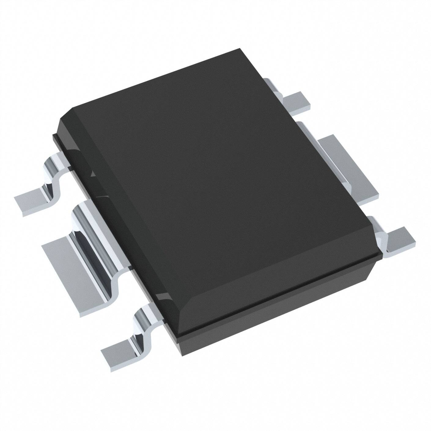
Since the packages for these ICs are high wattage HSOP-6J package, TO-252-5-P1, high density mounting of
the ICs on boards is possible.
FEATURES
• Supply Current ............................................................. Typ. 130μA
• Standby Current ........................................................... Typ. 0.1μA
• Output Current ............................................................. Min. 1.5A (VIN=VOUT+1.0V, R1171Sxx1A/B)
Min. 2.0A (VIN=VOUT+1.0V, R1171Jxx1C/D)
• Input Voltage ................................................................ 2.1V to 6.0V
• Output Voltage ............................................................. 1.5V to 5.0V (0.1V steps) (R1171Sxx1A/B)
1.8V to 5.0V (0.1V steps) (R1171Jxx1C/D)
(For other voltages, please refer to MARK INFORMATIONS.)
• Output Voltage Accuracy.............................................. ± 2.0%
• Dropout Voltage ........................................................... Typ. 0.09V (VOUT=3.0V, IOUT=300mA)
• Temperature-drift Coefficient of Output Voltage........... Typ. ± 100ppm/°C
• Line Regulation ............................................................ Typ. 0.05%/V
• Packages ..................................................................... HSOP-6J, TO-252-5-P1
• Built-in Current Limit Circuit
• Built-in Thermal Shutdown Circuit
• Ceramic capacitor for phase compensation ................ CIN=COUT=Ceramic 10μF (VOUT
= 1.8V)
APPLICATIONS
•
•
•
•
Local Power source for Notebook PC.
Local Power source for portable appliances, cameras, and videos.
Local Power source for equipment of battery-use.
Local Power source for home appliances.
1
�R1171x
BLOCK DIAGRAMS
R1171xxx1A/C
R1171xxx1B/D
VDD
VOUT
VDD
GND
Vref
VOUT
GND
Vref
Current Limit
Thermal Shutdown
Current Limit
Thermal Shutdown
CE
GND
CE
GND
SELECTION GUIDE
The output voltage, chip enable polarity, package for the ICs can be selected at the user’s request.
Product Name
R1171Sxx1∗-E2-FE
R1171Jyy1$-T1-F
Package
Quantity per Reel
Pb Free
Halogen Free
HSOP-6J
1,000 pcs
Yes
Yes
TO-252-5-P1
3,000 pcs
Yes
No
xx : The output voltage can be designated in the range from 1.5V(15) to 5.0V(50) in 0.1V steps.
(For other voltages, please refer to MARK INFORMATIONS.)
yy : The output voltage can be designated in the range from 1.8V(18) to 5.0V(50) in 0.1V steps.
(For other voltages, please refer to MARK INFORMATIONS.)
∗ : CE pin polarity are options as follows.
(A) "L" active
(B) "H" active
$ : CE pin polarity are options as follows.
(C) "L" active
(D) "H" active
2
�R1171x
PIN CONFIGURATIONS
6
z HSOP-6J
4
5
1
2
z TO-252-5-P1
3
1
2
3
4
5
PIN DESCRIPTIONS
•
•
HSOP-6J
Pin No
Symbol
Pin Description
1
VOUT
Output Pin
2
GND
Ground Pin
3
CE or CE
Chip Enable Pin
4
NC
No Connection
5
GND
6
VDD
Ground Pin
Input Pin
TO-252-5-P1
Pin No
Symbol
Pin Description
1
VOUT
2
CE or CE
3
GND
Ground Pin
4
GND
Ground Pin
5
VDD
Output Pin
Chip Enable Pin
Input Pin
∗) No.3 and No.4 pins must be wired short each other and connected to the GND plane when it is mounted on
board.
3
�R1171x
ABSOLUTE MAXIMUM RATINGS
Symbol
Item
Rating
Unit
7.0
V
VIN
Input Voltage
VCE
Input Voltage ( CE or CE Input Pin)
−0.3 to VIN+0.3
V
VOUT
Output Voltage
−0.3 to VIN+0.3
V
PD
Power Dissipation (HSOP-6J)∗1
1700
∗1
Power Dissipation (TO-252-5-P1)
mW
1900
Topt
Operating Temperature
−40 to 85
°C
Tstg
Storage Temperature
−55 to 125
°C
∗) For Power Dissipation, please refer to PACKAGE INFORMATION.
ABSOLUTE MAXIMUM RATINGS
Electronic and mechanical stress momentarily exceeded absolute maximum ratings may cause the
permanent damages and may degrade the life time and safety for both device and system using the device
in the field.
The functional operation at or over these absolute maximum ratings is not assured.
RECOMMENDED OPERATING CONDITIONS (ELECTRICAL CHARACTERISTICS)
All of electronic equipment should be designed that the mounted semiconductor devices operate within the
recommended operating conditions. The semiconductor devices cannot operate normally over the
recommended operating conditions, even if when they are used over such conditions by momentary
electronic noise or surge. And the semiconductor devices may receive serious damage when they continue
to operate over the recommended operating conditions.
4
�R1171x
ELECTRICAL CHARACTERISTICS
•
R1171Sxx1A
Topt=25°C
Symbol
VOUT
ΔVOUT/
ΔIOUT
VDIF
Item
Conditions
Min.
Output Voltage
VIN−VOUT=1.0V, IOUT=200mA
×0.98
Load Regulation
VIN−VOUT=1.0V
1mA <
= IOUT <
= 300mA
IOUT=300mA
Dropout Voltage
Typ.
Max.
Unit
×1.02
V
10
60
mV
1.5
<
=
VOUT
很抱歉,暂时无法提供与“R1171S331B-E2-FE”相匹配的价格&库存,您可以联系我们找货
免费人工找货