R1172x SERIES
SUPER LOW ON RESISTANCE / LOW VOLTAGE 1A LDO
NO.EA-122-070627
OUTLINE
The R1172x Series are CMOS-based positive voltage regulator ICs. The R1172x Series have features of super
low dropout, 1A output current capability. Even the output voltage is set at 1.5V, on resistance of internal FET is
typically 0.32Ω. Therefore, applications that require a large current at small dropout are suitable for the R1172x
series. Low input voltage is acceptable and low output voltage can be set. The minimum input voltage is 1.4V,
and the lowest set output voltage is 0.8V. Each of these ICs consists of a voltage reference unit, an error
amplifier, resistor net for setting output voltage, a current limit circuit at over-current, a chip enable circuit, a
thermal-shutdown circuit, and so on. A stand-by mode with ultra low consumption current can be realized with
the chip enable pin. The output voltage of R1172 is fixed in the IC.
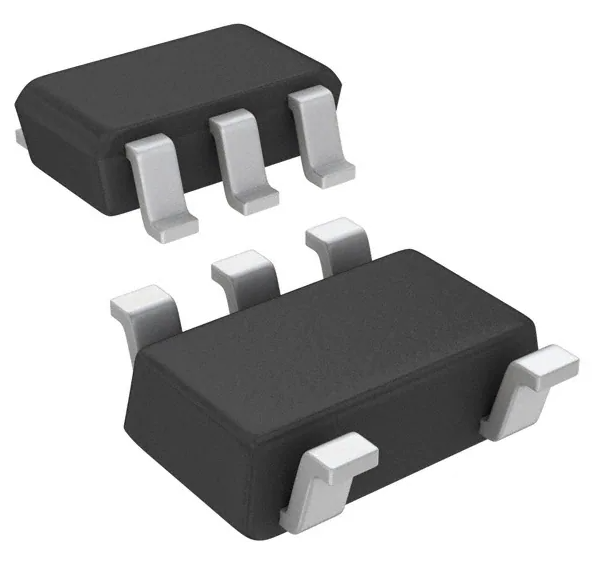
Since the packages for these ICs are SOT-23-5, SOT-89-5, HSON-6, and HSOP-6J with high power
dissipation, high density mounting of the ICs on boards is possible.
FEATURES
•
•
•
•
•
•
•
•
•
•
•
•
•
•
•
•
•
Output Current ............................................................ 1A
Supply Current ............................................................. Typ. 60µA
Standby Current .......................................................... Typ. 0.1µA
Input Voltage Range ................................................... 1.4V to 6.0V
Output Voltage.............................................................. Stepwise setting with a step of 0.1V in the range of
0.8V to 5.0V (Exceptions: HSOP-6J = 0.8V to 3.5V)
Dropout Voltage............................................................ Typ. 0.32V (VOUT=1.5V, IOUT=1A)
Typ. 0.18V (VOUT=2.8V, IOUT=1A)
Ripple Rejection ........................................................... Typ. 70dB (VOUT=2.8V)
Output Voltage Accuracy.............................................. ±2.0%
Temperature-Drift Coefficient of Output Voltage .......... Typ. ±100ppm/°C
Line Regulation ............................................................ Typ. 0.05%/V
Load Regulation ......................................................... Typ. 15mV at IOUT=300mA, Typ. 50mV at IOUT=1A
Packages .................................................................... SOT-23-5, SOT-89-5, HSON-6, HSOP-6J
Built-in Inrush current limit circuit ............................... Typ. 500 mA
Built-in Fold-Back Protection Circuit ........................... Typ. 250mA (Current at short mode)
Built-in Thermal Shutdown Circuit .............................. Thermal Shutdown Temperature ; Typ. 150°C
Released Temperature ; Typ. 120°C
Built-in Auto Discharge Function ................................ D version
Output capacitors ....................................................... CIN=COUT=Tantalum 4.7µF (VOUT < 1.0V)
CIN=COUT=Ceramic 4.7µF (VOUT >
= 1.0V)
APPLICATIONS
• Local Power source for Notebook PC.
• Local Power source for portable communication equipments, cameras, and VCRs.
• Local Power source for home appliances.
1
�R1172x
BLOCK DIAGRAMS
R1172xxx1A
VDD
VOUT
Vref
Current Limit
Thermal Shutdown
CE
GND
R1172xxx1B
VDD
R1172xxx1D
VOUT
VDD
VOUT
Vref
Vref
Current Limit
Thermal Shutdown
Current Limit
Thermal Shutdown
CE
GND
CE
GND
SELECTION GUIDE
The output voltage, auto discharge function*, and the package type for the ICs can be selected at the user’s
request. The selection can be made with designating the part number as shown below;
R1172xxx1x-xx-x ←Part Number
↑ ↑
a b
Code
a
b
c
↑ ↑ ↑
c d e
Contents
Designation of Package Type;
N: SOT-23-5, H: SOT-89-5, D: HSON-6, S: HSOP-6J
Setting Output Voltage (VOUT);
Stepwise setting with a step of 0.1V in the range of 0.8V to 5.0V (HSOP-6J : 0.8V to 3.5V)
is possible.
Exceptions; 1.85V output: R1172x181x5-xx-x, 2.85V output: R1172x281x5-xx-x
Designation of option;
A: active low, without auto discharge function*
B: active high, without auto discharge function*
D: active high, with auto discharge function*
d
Designation of Taping Type;
T1 (SOT-89-5), TR (SOT-23-5, HSON-6), E2 (HSOP-6J) Refer to Taping Specifications.
e
Designation of composition of pin plating;
-F: Lead free plating
*) When the mode is into standby with CE signal, auto discharge transistor turns on, and it makes the turn-off
speed faster than normal type.
2
�R1172x
PIN CONFIGURATIONS
SOT-23-5
SOT-89-5
5
5
4
4
(mark side)
1
2
1
3
HSON-6
Top View
6
5
4
1
2
5
3
3
6
5
4
1
2
3
6
∗
∗
3
HSOP-6J
Bottom View
4
2
∗
2
1
PIN DESCRIPTIONS
• SOT-23-5
• SOT-89-5
Pin No.
Symbol
Description
Pin No.
Symbol
1
VOUT
Voltage Regulator Output Pin
1
CE or CE
2
GND
Ground Pin
2
GND
3
VDD
Input Pin
3
NC
No Connection
4
NC
No Connection
4
VDD
Input Pin
5
CE or CE
Chip Enable Pin
5
VOUT
Voltage Regulator Output Pin
• HSON-6*1
Description
Chip Enable Pin
Ground Pin
• HSOP-6J
Pin No.
Symbol
Description
Pin No.
Symbol
Description
1
VOUT*2
Voltage Regulator Output Pin
1
VOUT
Voltage Regulator Output Pin
2
2
VOUT*
Voltage Regulator Output Pin
2
GND
Ground Pin
3
CE or CE
Chip Enable Pin
3
CE or CE
Chip Enable Pin
4
GND
Ground Pin
4
NC
No Connection
5
VDD
Input Pin
5
GND
6
VDD
Input Pin
6
VDD
Ground Pin
Input Pin
*1) Tab in the
parts have GND level. (They are connected to the reverse side of this IC.)
Do not connect to other wires or land patterns.
*2) Connect Pin1 and Pin2 as short as possible.
3
�R1172x
ABSOLUTE MAXIMUM RATINGS
Symbol
Item
Rating
Unit
6.5
V
−0.3 to 6.5
V
VIN
Input Voltage
VCE
Input Voltage ( CE or CE Input Pin)
VOUT
Output Voltage
−0.3 to VIN+0.3
V
IOUT
Output Current
1.4
A
Power Dissipation (SOT-23-5) *
420
Power Dissipation (SOT-89-5) *
900
Power Dissipation (HSON-6) *
900
Power Dissipation (HSOP-6J) *
1700
Topt
Operating Temperature Range
−40 to 85
°C
Tstg
Storage Temperature Range
−55 to 125
°C
PD
*) For Power Dissipation, please refer to PACKAGE INFORMATION to be described.
(Includes additional information of High Wattage Land Pattern)
4
mW
�R1172x
ELECTRICAL CHARACTERISTICS
•
R1172xxx1A
Symbol
Topt=25°C
Item
Conditions
Min.
Typ.
Unit
6.0
V
VIN
Input Voltage
ISS
Supply Current
VIN−VOUT=1.0V, VCE=0V,
IOUT =0A
60
100
µA
Standby Current
VIN= 6.0V, VCE=VIN
0.1
1.0
µA
VOUT
Output Voltage
VIN−VOUT=1.0V
IOUT=100mA
×0.98
×1.02
V
−30
+30
mV
IOUT
Output Current
VIN−VOUT=1.0V
Istandby
∆VOUT/
∆IOUT
VDIF
Load Regulation
1.4
Max.
VOUT > 1.5V
VOUT <
=
1.5V
1
VIN−VOUT=0.3V
1mA <
= IOUT <
= 300mA
If VOUT <
= 1.1V, then VIN=1.4V
−15
Refer to Dropout Voltage Table
Line Regulation
Ripple Rejection
f=1kHz (VOUT <
= 4.0V)
f=1kHz (VOUT > 4.0V)
Ripple 0.5Vp-p, VIN−VOUT=1.0V,
IOUT=100mA
If VOUT <
= 1.2V, VIN−VOUT=1.5V,
IOUT=100mA
Output Voltage
Temperature Coefficient
IOUT=100mA
−40°C <
= Topt
Ilim
Short Current Limit
VOUT=0V
RPU
Pull-up Resistance for CE pin
1.9
VCEH
CE Input Voltage "H"
VCEL
CE Input Voltage "L"
RR
∆VOUT/
∆Topt
TTSD
TTSR
en
Thermal Shutdown
Temperature
Thermal Shutdown
Released Temperature
Output Noise
30
50
IOUT=100mA
VOUT+0.5V <
= VIN <
= 6.0V
<
If VOUT = 0.9V,
1.4V <
= VIN <
= 6.0V
∆VOUT/
∆VIN
15
mV
VIN−VOUT=0.3V
1mA <
= IOUT <
= 1A
If VOUT <
= 1.1V, then VIN=1.7V
Dropout Voltage
A
<
=
0.05
0.20
%/V
70
60
dB
85°C
±100
ppm/°C
250
mA
5.0
15.0
MΩ
1.0
6.0
V
0
0.4
V
Junction Temperature
150
°C
Junction Temperature
120
°C
BW=10Hz to 100kHz
30
µVrms
5
�R1172x
•
R1172xxx1B/D
Symbol
Item
Conditions
Min.
Typ.
Unit
6.0
V
Input Voltage
ISS
Supply Current
VIN−VOUT=1.0V, VIN=VCE,
IOUT=0A
60
100
µA
Standby Current
VIN= 6.0V, VCE=0V
0.1
1.0
µA
VOUT
Output Voltage
VIN−VOUT=1.0V
IOUT=100mA
IOUT
Output Current
VIN−VOUT=1.0V
∆VOUT/
∆IOUT
VDIF
Load Regulation
1.4
Max.
VIN
Istandby
VOUT > 1.5V
×0.98
×1.02
V
<
=
−30
+30
mV
VOUT
1.5V
1
VIN−VOUT=0.3V
1mA <
= IOUT <
= 300mA
If VOUT <
1.1V,
then VIN=1.4V
=
−15
Dropout Voltage
Ripple Rejection
Output Voltage
Temperature Coefficient
IOUT=100mA
−40°C <
= Topt
Ilim
Short Current Limit
VOUT=0V
RPD
Pull-down Resistance for CE
pin
1.9
VCEH
CE Input Voltage "H"
VCEL
CE Input Voltage "L"
TTSD
TTSR
en
Thermal Shutdown
Temperature
Thermal Shutdown
Released Temperature
Output Noise
30
Refer to Dropout Voltage Table
f=1kHz (VOUT <
= 4.0V)
f=1kHz (VOUT > 4.0V)
Ripple 0.5Vp-p, VIN−VOUT=1.0V
IOUT=100mA
If VOUT <
= 1.2V, VIN−VOUT=1.5V,
IOUT=100mA
∆VOUT/
∆Topt
15
50
Line Regulation
RR
A
mV
VIN−VOUT=0.3V
1mA <
= IOUT <
= 1A
If VOUT <
= 1.1V, then VIN=1.7V
IOUT=100mA
VOUT+0.5V <
= VIN <
= 6.0V
If VOUT <
0.9V,
=
1.4V <
= VIN <
= 6.0V
∆VOUT/
∆VIN
6
Topt=25°C
<
=
0.05
0.20
%/V
70
60
dB
85°C
±100
ppm/°C
250
mA
5.0
15.0
MΩ
1.0
6.0
V
0
0.4
V
Junction Temperature
150
°C
Junction Temperature
120
°C
BW=10Hz to 100kHz
30
µVrms
�R1172x
•
Dropout Voltage by Output Voltage
Topt=25°C
Dropout Voltage VDIF (V)
Output Voltage
VOUT (V)
IOUT=300mA
IOUT=1A
Typ.
Max.
Typ.
0.8
<
=
VOUT < 0.9
0.33
0.57
0.72
0.9
<
=
VOUT < 1.0
0.22
0.47
0.64
1.0
<
=
VOUT < 1.5
0.18
0.32
0.56
1.5
<
=
VOUT < 2.6
0.10
0.15
0.32
0.05
0.10
0.18
2.6
<
=
VOUT
7
�R1172x
TYPICAL APPLICATION (R1172xxx1B/D)
VDD
C1
VOUT
VOUT
R1172x
Series
CE
C2
GND
TECHNICAL NOTES
When using these ICs, consider the following points:
Phase Compensation
In these ICs, phase compensation is made for securing stable operation even if the load current is varied. For
this purpose, use a capacitor C2 with good frequency characteristics and ESR (Equivalent Series Resistance).
The recommendation value is as follows.
Output Voltage C2 recommendation value
VOUT < 1.0V
Tantalum 4.7µF or more
1.0
<
=
VOUT
<
=
3.3V
3.3V < VOUT
Ceramic 4.7µF or more
Ceramic 4.7µF or more
Components Recommendation
Kyocera 4.7µF (1608)
Murata 4.7µF (1608)
Murata 10µF (1608)
Kyocera 4.7µF (thin 2012)
Murata 10µF (2012)
Part Number : CM105X5R475M06AB
Part Number : GRM188R60J475KE19B
Part Number : GRM188B30G106ME46B
Part Number : CT21X5R475M06AB
Part Number : GRM21BB30J106K
∗ If you use a tantalum type capacitor and ESR value of the capacitor is large, output might be unstable.
Evaluate your circuit with considering frequency characteristics.
∗ Depending on the capacitor size, manufacturer, and part number, the bias characteristics and temperature
characteristics are different. Evaluate the circuit with actual using capacitors.
PCB Layout
Make VDD and GND lines sufficient. If their impedance is high, noise pickup or unstable operation may result.
Connect a capacitor C1 with a capacitance value as much as 4.7µF or more between VDD and GND pin, and as
close as possible to the pins.
Set external components, especially the output capacitor C2, as close as possible to the ICs, and make wiring
as short as possible.
8
�R1172x
TYPICAL CHARACTERISTICS
1) Output Voltage vs. Output Current (Topt=25°C)
R1172x151x
1.6
0.8
1.4
0.7
0.6
0.5
0.4
VDD=1.4V
VDD=1.5V
VDD=1.6V
VDD=2.0V
VDD=2.8V
0.3
0.2
0.1
Output Voltage VOUT(V)
Output Voltage VOUT(V)
R1172x081x
0.9
0.0
1.2
1.0
0.8
0.6
VDD=1.8V
VDD=2.5V
VDD=3.5V
0.4
0.2
0.0
0
500
1000
1500
Output Current IOUT(mA)
2000
0
4.5
2.8
4.0
2.4
2.0
1.6
1.2
VDD=3.3V
VDD=4.0V
VDD=5.0V
0.8
0.4
0.0
0
2000
R1172x401x
3.2
500
1000
1500
Output Current IOUT(mA)
2000
Output Voltage VOUT(V)
Output Voltage VOUT(V)
R1172x301x
500
1000
1500
Output Current IOUT(mA)
3.5
3.0
2.5
2.0
VDD=4.3V
VDD=5.0V
VDD=6.0V
1.5
1.0
0.5
0.0
0
500
1000
1500
Output Current IOUT(mA)
2000
R1172x501x
Output Voltage VOUT(V)
6.0
5.0
4.0
3.0
VDD=5.3V
VDD=6.0V
2.0
1.0
0.0
0
500
1000
1500
Output Current IOUT(mA)
2000
9
�R1172x
2) Output Voltage vs. Input Voltage (Topt=25°C)
R1172x081x
R1172x151x
1.6
Output Voltage VOUT(V)
Output Voltage VOUT(V)
1.2
1.0
0.8
0.6
IOUT=1mA
IOUT=50mA
IOUT=99mA
IOUT=300mA
0.4
0.2
0.0
1.4
1.2
1.0
0.8
IOUT=1mA
IOUT=50mA
IOUT=99mA
IOUT=300mA
0.6
0.4
0.2
0.0
0
1
2
3
4
Input Voltage VIN(V)
5
6
0
1
4.5
2.8
4.0
2.4
2.0
1.6
IOUT=1mA
IOUT=50mA
IOUT=99mA
IOUT=300mA
1.2
0.8
0.4
0.0
1
2
3
4
Input Voltage VIN(V)
5
6
R1172x501x
Output Voltage VOUT(V)
6
3.5
3.0
2.5
2.0
IOUT=1mA
IOUT=50mA
IOUT=99mA
IOUT=300mA
1.5
1.0
0.5
0.0
0
5.5
5.0
4.5
4.0
3.5
3.0
2.5
2.0
1.5
1.0
0.5
0.0
IOUT=1mA
IOUT=50mA
IOUT=99mA
IOUT=300mA
0
10
5
R1172x401x
3.2
Output Voltage VOUT(V)
Output Voltage VOUT(V)
R1172x301x
2
3
4
Input Voltage VIN(V)
1
2
3
4
Input Voltage VIN(V)
5
6
0
1
2
3
4
Input Voltage VIN(V)
5
6
�R1172x
3) Supply Current vs. Input Current (Topt=25°C)
R1172x151x
70
70
60
60
Supply Current ISS(µA)
Supply Current ISS(µA)
R1172x081x
50
40
30
20
10
0
0
1
2
3
4
Input Voltage VIN(V)
5
50
40
30
20
10
0
6
0
1
70
60
60
50
40
30
20
10
0
0
1
2
3
4
Input Voltage VIN(V)
5
6
5
6
R1172x401x
70
Supply Current ISS(µA)
Supply Current ISS(µA)
R1172x301x
2
3
4
Input Voltage VIN(V)
5
6
5
6
50
40
30
20
10
0
0
1
2
3
4
Input Voltage VIN(V)
R1172x501x
Supply Current ISS(µA)
70
60
50
40
30
20
10
0
0
1
2
3
4
Input Voltage VIN(V)
11
�R1172x
4) Output Voltage vs. Temperature (IOUT=100mA)
R1172x081x
VIN=1.8V
0.83
0.82
0.81
0.80
0.79
0.78
0.77
0.76
-50
-25
0
25
50
75
Temperature Topt(°C)
VIN=2.5V
1.53
Output Voltage VOUT(V)
Output Voltage VOUT(V)
R1172x151x
1.52
1.51
1.50
1.49
1.48
1.47
1.46
-50
100
-25
R1172x301x
3.02
3.00
2.98
2.96
2.94
-25
0
25
50
75
Temperature Topt(°C)
VIN=6.0V
5.02
Output Voltage VOUT(V)
Output Voltage VOUT(V)
3.04
2.92
-50
100
R1172x501x
VIN=4.0V
3.06
0
25
50
75
Temperature Topt(°C)
5.00
4.98
4.96
4.94
4.92
4.90
4.88
-50
100
-25
0
25
50
75
Temperature Topt(°C)
100
5) Supply Current vs. Temperature
R1172x081x
VIN=1.8V
70
60
50
40
30
20
10
0
-50
VIN=2.5V
80
Supply Current ISS(µA)
Supply Current ISS(µA)
80
12
R1172x151x
-25
0
25
50
75
Temperature Topt(°C)
100
70
60
50
40
30
20
10
0
-50
-25
0
25
50
75
Temperature Topt(°C)
100
�R1172x
R1172x301x
80
VIN=6.0V
80
70
Supply Current ISS(µA)
Supply Current ISS(µA)
R1172x501x
VIN=4.0V
60
50
40
30
20
10
0
-50
-25
0
25
50
75
Temperature Topt(°C)
70
60
50
40
30
20
10
0
-50
100
-25
0
25
50
75
Temperature Topt(°C)
100
6) Dropout Voltage vs. Output Current
R1172x091x
700
700
600
600
500
400
300
85°C
25°C
-40°C
200
100
0
0
200
400
600
800
Output Current IOUT(mA)
Dropout Voltage VDIF(mV)
Dropout Voltage VDIF(mV)
R1172x081x
800
500
400
300
100
0
1000
85°C
25°C
-40°C
200
0
600
400
500
350
400
300
85°C
25°C
-40°C
200
100
0
0
1000
R1172x151x
200
400
600
800
Output Current IOUT(mA)
1000
Dropout Voltage VDIF(mV)
Dropout Voltage VDIF(mV)
R1172x101x
200
400
600
800
Output Current IOUT(mA)
300
250
200
150
85°C
25°C
-40°C
100
50
0
0
200
400
600
800
Output Current IOUT(mA)
1000
13
�R1172x
R1172x301x
R1172x501x
Dropout Voltage VDIF(mV)
Dropout Voltage VDIF(mV)
250
200
150
100
85°C
25°C
-40°C
50
0
0
200
400
600
800
Output Current IOUT(mA)
200
180
160
140
120
100
80
60
40
20
0
1000
7) Dropout Voltage vs. Set Output Voltage
85°C
25°C
-40°C
0
200
400
600
800
Output Current IOUT(mA)
8) 0.8V Output type, Operating Input Voltage Range
R1172xxx1x
R1172x081x
800
1.8
100mA
200mA
400mA
600mA
800mA
1000mA
700
600
500
400
Input Voltage VIN(V)
Dropout Voltage VDIF(mV)
1000
300
200
Operating Input Voltage Range
1.6
1.4
1.2
1.0
100
0
0.8
0
1
2
3
4
Set Output Voltage VREG(V)
5
0
200
400
600
800
Output Current IOUT(mA)
1000
9) Ripple Rejection vs. Input Bias
R1172x301x
80
70
60
50
40
200Hz
1kHz
10kHz
1000kHz
30
20
10
0
3.0
14
VIN=4.0VDC+0.2Vp-p,IOUT=1mA
3.1
3.2
3.3
3.4
Input Voltage VIN(V)
90
Ripple Rejection RR(dB)
Ripple Rejection RR(dB)
90
R1172x301x
3.5
VIN=4.0VDC+0.5Vp-p,IOUT=1mA
80
70
60
50
40
200Hz
1kHz
10kHz
1000kHz
30
20
10
0
3.0
3.1
3.2
3.3
3.4
Input Voltage VIN(V)
3.5
�R1172x
R1172x301x
80
70
60
50
40
200Hz
1kHz
10kHz
1000kHz
30
20
10
0
3.0
3.1
3.2
3.3
3.4
Input Voltage VIN(V)
90
Ripple Rejection RR(dB)
Ripple Rejection RR(dB)
90
R1172x301x
VIN=4.0VDC+0.2Vp-p,IOUT=10mA
80
70
60
50
40
200Hz
1kHz
10kHz
1000kHz
30
20
10
0
3.0
3.5
VIN=4.0VDC+0.5Vp-p,IOUT=10mA
3.1
R1172x301x
VIN=4.0VDC+0.2Vp-p,IOUT=100mA
90
80
70
60
50
40
200Hz
1kHz
10kHz
1000kHz
30
20
10
0
3.0
3.1
3.5
R1172x301x
Ripple Rejection RR(dB)
Ripple Rejection RR(dB)
90
3.2
3.3
3.4
Input Voltage VIN(V)
3.2
3.3
3.4
Input Voltage VIN(V)
80
200Hz
1kHz
10kHz
1000kHz
70
60
50
40
30
20
10
0
3.0
3.5
VIN=4.0VDC+0.5Vp-p,IOUT=100mA
3.1
3.2
3.3
3.4
Input Voltage VIN(V)
3.5
10) Ripple Rejection vs. Frequency
R1172x081x
R1172x101x
VIN=2.0VDC+0.5Vp-p,
COUT=Ceramic 0.47µF
80
90
70
80
Ripple Rejection RR(dB)
Ripple Rejection RR(dB)
VIN=1.8VDC+0.5Vp-p,
COUT=Tantalum 0.47µF
60
50
40
30
20
10
0
0.1
IOUT=1mA
IOUT=30mA
IOUT=100mA
1
10
Frequency f(kHz)
100
70
60
50
40
30
20
10
0
0.1
IOUT=1mA
IOUT=30mA
IOUT=100mA
1
10
Frequency f(kHz)
100
15
�R1172x
R1172x301x
R1172x401x
VIN=5.0VDC+0.5Vp-p,
COUT=Ceramic 0.47µF
90
90
80
80
Ripple Rejection RR(dB)
Ripple Rejection RR(dB)
VIN=4.0VDC+0.5Vp-p,
COUT=Ceramic 0.47µF
70
60
50
40
30
20
10
0
0.1
IOUT=1mA
IOUT=30mA
IOUT=100mA
1
10
Frequency f(kHz)
100
70
60
50
40
30
10
0
0.1
R1172x451x
70
70
Ripple Rejection RR(dB)
Ripple Rejection RR(dB)
80
60
50
40
30
IOUT=1mA
IOUT=30mA
IOUT=100mA
0
0.1
1
10
Frequency f(kHz)
100
VIN=6.0VDC+0.5Vp-p,
COUT=Ceramic 0.47µF
80
10
1
10
Frequency f(kHz)
R1172x501x
VIN=5.5VDC+0.5Vp-p,
COUT=Ceramic 0.47µF
20
IOUT=1mA
IOUT=30mA
IOUT=100mA
20
60
50
40
30
20
IOUT=1mA
IOUT=30mA
IOUT=100mA
10
0
0.1
100
1
10
Frequency f(kHz)
100
11) Line Transient Response (tr=tf=5µs, IOUT=100mA)
R1172x081x
R1172x101x
COUT=Tantalum 4.7µF
3
1.08
3
0.86
2
0.84
1
0.82
0
0.80
0.78
Output Voltage
0.76
1.06
Input Voltage
1.04
1.02
2
1
0
Output Voltage
1.00
0.98
0.96
0 10 20 30 40 50 60 70 80 90 100
Time t(µs)
16
4
0 10 20 30 40 50 60 70 80 90 100
Time t(µs)
Input Voltage VIN(V)
Input Voltage
1.10
Output Voltage VOUT(V)
0.88
COUT=Ceramic 4.7µF
4
Input Voltage VIN(V)
Output Voltage VOUT(V)
0.90
�R1172x
R1172x301x
R1172x501x
COUT=Ceramic 4.7µF
5.15
3.12
5
5.12
3.09
Input Voltage
4
3.06
3
3.03
2
3.00
1
2.97
0
Output Voltage
2.94
7
6
Input Voltage
5.09
5
5.06
4
5.03
3
5.00
2
4.97
1
Output Voltage
0
4.94
0 10 20 30 40 50 60 70 80 90 100
Time t(µs)
Input Voltage VIN(V)
6
Output Voltage VOUT(V)
3.15
Input Voltage VIN(V)
Output Voltage VOUT(V)
COUT=Ceramic 4.7µF
0 10 20 30 40 50 60 70 80 90 100
Time t(µs)
12) Load Transient Response (tr=tf=500ns)
R1172x081x
Output Current
0.92
200
0.86
0
0.80
Output Voltage
0.68
Output Current
0.92
0.88
50
0
0.84
Output Voltage
0.80
0.76
0
R1172x081x
0
0.84
0.80
Output Voltage VOUT(V)
20
Output Current
0.88
6
8 10 12 14 16 18 20
Time t(µs)
1.00
40
0.92
4
VIN=1.8V,CIN=Tantalum 4.7µF,
COUT=Tantalum 10µF
VIN=1.8V,CIN=COUT= Tantalum 4.7µF
0.96
2
R1172x081x
Output Current IOUT(mA)
Output Voltage VOUT(V)
100
0.96
0 10 20 30 40 50 60 70 80 90 100
Time t(µs)
1.00
150
40
0.96
20
Output Current
0
0.92
0.88
0.84
0.80
Output Current IOUT(mA)
0.74
Output Voltage VOUT(V)
400
0.98
VIN=1.8V,CIN=COUT= Tantalum 4.7µF
1.00
600
Output Current IOUT(mA)
VIN=1.8V,CIN=COUT= Tantalum 4.7µF
Output Current IOUT(mA)
Output Voltage VOUT(V)
1.04
R1172x081x
Output Voltage
Output Voltage
0.76
0.76
0 10 20 30 40 50 60 70 80 90 100
Time t(µs)
0 10 20 30 40 50 60 70 80 90 100
Time t(µs)
17
�R1172x
R1172x101x
1.4
Output Current
1.2
200
1.1
0
1.0
0.9
Output Voltage
Output Voltage VOUT(V)
400
1.3
Output Current IOUT(mA)
600
1.2
200
1.1
0
1.0
0.9
R1172x101x
R1172x101x
100
1.16
Output Current
1.12
1.08
50
0
1.04
Output Voltage
1.00
Output Voltage VOUT(V)
150
1.20
150
1.16
100
Output Current
1.12
1.08
50
0
1.04
Output Voltage
1.00
Output Current IOUT(mA)
VIN=2.0V,CIN=Ceramic 4.7µF,
COUT=Ceramic 10µF
VIN=2.0V,CIN=COUT= Ceramic 4.7µF
0.96
0.96
4
8
0
12 16 20 24 28 32 36 40
Time t(µs)
R1172x101x
1.00
0.95
Output Voltage VOUT(V)
0
Output Voltage
8 10 12 14 16 18 20
Time t(µs)
1.20
Output Current IOUT(mA)
20
Output Current
1.05
6
R1172x101x
40
1.10
4
VIN=2.0V,CIN=Ceramic 4.7µF,
COUT=Ceramic 10µF
VIN=2.0V,CIN=COUT= Ceramic 4.7µF
1.15
2
40
1.15
20
Output Current
0
1.10
1.05
Output Voltage
1.00
0.95
0.90
0.90
0 10 20 30 40 50 60 70 80 90 100
Time t(µs)
0 10 20 30 40 50 60 70 80 90 100
Time t(µs)
Output Current IOUT(mA)
0
Output Voltage VOUT(V)
Output Voltage
0 10 20 30 40 50 60 70 80 90 100
Time t(µs)
Output Current IOUT(mA)
Output Voltage VOUT(V)
Output Current
0 10 20 30 40 50 60 70 80 90 100
Time t(µs)
1.20
18
400
1.3
0.8
0.8
1.20
600
Output Current IOUT(mA)
VIN=2.0V,CIN=COUT= Ceramic 4.7µF
1.4
Output Voltage VOUT(V)
R1172x101x
VIN=2.0V,CIN=Ceramic 4.7µF,
COUT=Ceramic 10µF
�R1172x
R1172x301x
VIN=4.0V,CIN=COUT= Ceramic 4.7µF
3.4
200
3.2
0
3.0
2.8
Output Voltage
Output Voltage VOUT(V)
Output Current
Output Current IOUT(mA)
400
3.6
3.8
2.6
600
400
3.6
Output Current
3.4
200
3.2
0
3.0
2.8
Output Voltage
2.6
0 40 80 120 160 200 240 280 320 360 400
Time t(µs)
0 40 80 120 160 200 240 280 320 360 400
Time t(µs)
R1172x301x
VIN=4.0V,CIN=Ceramic 4.7µF,
COUT=Ceramic 10µF
100
3.16
Output Current
3.12
50
3.08
0
3.04
Output Voltage
3.00
Output Voltage VOUT(V)
150
Output Current IOUT(mA)
3.20
150
3.16
100
3.08
0
4
Output Voltage
3.00
0
8 12 16 20 24 28 32 36 40
Time t(µs)
0
3.00
Output Voltage
Output Voltage VOUT(V)
20
Output Current
3.05
6
8 10 12 14 16 18 20
Time t(µs)
3.20
40
3.10
4
R1172x301x
VIN=4.0V,CIN=COUT= Ceramic 4.7µF
3.15
2
VIN=4.0V,CIN=Ceramic 4.7µF,
COUT=Ceramic 10µF
Output Current IOUT(mA)
Output Voltage VOUT(V)
0
3.04
R1172x301x
2.95
50
2.96
2.96
3.20
Output Current
3.12
40
20
3.15
Output Current
0
3.10
3.05
3.00
2.95
Output Voltage
Output Current IOUT(mA)
Output Voltage VOUT(V)
R1172x301x
VIN=4.0V,CIN=COUT= Ceramic 4.7µF
3.20
Output Current IOUT(mA)
600
Output Current IOUT(mA)
3.8
Output Voltage VOUT(V)
R1172x301x
VIN=4.0V,CIN=Ceramic 4.7µF,
COUT=Ceramic 10µF
2.90
2.90
0 40 80 120 160 200 240 280 320 360 400
Time t(µs)
0 40 80 120 160 200 240 280 320 360 400
Time t(µs)
19
�R1172x
R1172x501x
5.50
200
5.25
0
5.00
4.75
Output Voltage
4.50
150
100
5.16
Output Current
5.12
50
5.08
0
5.04
Output Voltage
5.00
Output Current IOUT(mA)
Output Current
Output Voltage VOUT(V)
400
5.75
VIN=6.0V,CIN=COUT= Ceramic 4.7µF
5.20
600
Output Current IOUT(mA)
Output Voltage VOUT(V)
6.00
R1172x501x
VIN=6.0V,CIN=COUT= Ceramic 4.7µF
4.96
0
0 40 80 120 160 200 240 280 320 360 400
Time t(µs)
2
4
6
8 10 12 14 16 18 20
Time t(µs)
R1172x501x
VIN=6.0V,CIN=COUT= Ceramic 4.7µF
40
20
5.15
Output Current
0
5.10
5.05
5.00
4.95
Output Voltage
Output Current IOUT(mA)
Output Voltage VOUT(V)
5.20
4.90
0 40 80 120 160 200 240 280 320 360 400
Time t(µs)
13) Turn-on speed with CE pin control
-20 0
20
20 40 60 80 100 120 140 160 180
Time t(µs)
10
VIN=6.0V,CIN=COUT= Ceramic 4.7µF
8
8
6
6
4
4
2
2
IOUT=0mA
IOUT=100mA
IOUT=300mA
VIN(V)
0
-40 0
60
160
Time t(µs)
260
360
0
CE Input Voltage VCE(V)
IOUT=0mA
IOUT=100mA
IOUT=300mA
VCE
2.0
1.6
1.2
0.8
0.4
0.0
Output Voltage VOUT(V)
1.8
1.6
1.4
1.2
1.0
0.8
0.6
0.4
0.2
0.0
R1172x501x
CE Input Voltage VCE(V)
Output Voltage VOUT(V)
R1172x081x
VIN=1.8V,CIN=COUT= Tantalum 4.7µF
�R1172x
14) Turn-off speed with CE pin control
2.0
1.6
1.2
0.8
0.4
0.0
IOUT=0mA
IOUT=100mA
IOUT=300mA
VIN(V)
-0.4 0
0.6
1.6
Time t(ms)
2.8
14
VIN=6.0V,CIN=COUT= Tantalum 4.7µF
8
12
6
10
4
8
2
6
CE Input Voltage VCE(V)
VIN=1.8V,CIN=COUT= Tantalum 4.7µF
Output Voltage VOUT(V)
2.0
1.8
1.6
1.4
1.2
1.0
0.8
0.6
0.4
0.2
0.0
R1172x501D
CE Input Voltage VCE(V)
Output Voltage VOUT(V)
R1172x081D
0
IOUT=0mA
IOUT=100mA
IOUT=300mA
VIN(V)
4
2
0
3.6
-0.2 0 0.2
0.6
1.0
Time t(ms)
1.4
1.8
15) Inrush Current (IOUT=100mA, CIN=none)
1.6
CE Input Voltage
0.8
0.0
Output Voltage
600
400
200
0
Inrush Current
-40
0
40
80
Time t(µs)
120
160
2.4
VIN=2.0V,COUT= Tantalum 10µF
1.6
CE Input Voltage
0.8
0.0
Output Voltage
600
400
200
0
Inrush Current
-40
0
40
80
Time t(µs)
120
Inrush Current IVDD(mA)
VIN=2.0V,COUT= Tantalum 4.7µF
CE Input Voltage VCE ,Output Voltage VOUT(V)
2.4
R1172x081x
Inrush Current IVDD(mA)
CE Input Voltage VCE ,Output Voltage VOUT(V)
R1172x081x
160
21
�R1172x
CE Input Voltage
3
2
Output Voltage
1
0
600
400
Inrush Current
200
0
-40
0
40
80
Time t(µs)
120
5
4
CE Input Voltage
3
2
Output Voltage
1
0
600
400
Inrush Current
200
0
160
-40
0
CE Input Voltage
6
4
Output Voltage
2
0
600
400
Inrush Current
200
0
-40
22
0
40
80
Time t(µs)
120
160
CE Input VoltageVCE ,Output Voltage VOUT(V)
VIN=6.0V,COUT= Ceramic 4.7µF
8
120
160
R1172x501x
Inrush Current IVDD(mA)
CE Input VoltageVCE ,Output Voltage VOUT(V)
R1172x501x
40
80
Time t(µs)
Inrush Current IVDD(mA)
4
VIN=4.0V,COUT= Ceramic 10µF
VIN=6.0V,COUT= Ceramic 10µF
8
CE Input Voltage
6
4
Output Voltage
2
0
600
Inrush Current
400
200
0
-40
0
40
80
Time t(µs)
120
160
Inrush Current IVDD(mA)
5
CE Input VoltageVCE ,Output Voltage VOUT(V)
R1172x301x
Inrush Current IVDD(mA)
CE Input Voltage VCE ,Output Voltage VOUT(V)
R1172x301x
VIN=4.0V,COUT= Ceramic 4.7µF
�R1172x
ESR vs. Output Current
When using these ICs, consider the following points:
CE
VOUT
R1172xxx1B
COUT
S.A Spectrum
Analyzer
VIN
VIN
GND
CIN
ESR
IOUT
0.8V to 3.3V Output type: COUT=4.7µF (Kyocera CM105X5R475M06AB)
5.0V Output type
: COUT=4.7µF (Kyocera CT21X5R475K06AB)
As an output capacitor for this IC, Ceramic capacitor is recommendable. However, other low ESR type
capacitor can be used with this IC.
For your reference, noise level is tested, and if the noise level is 40µV or less than 40µV, the ESR values are
plotted as stable area. Upper limit is described in the next five graphs, or ESR vs. Output Current. (Hatched area
is the stable area.)
Measurement conditions
⋅ VIN=VOUT+1V
⋅ Frequency Band: 10Hz to 1MHz
⋅ Temperature : 25°C
R1172x081x
R1172x081x
VIN=1.4V to 6.0V,
CIN=COUT=Ceramic 4.7µF
VIN=1.4V to 6.0V, CIN=Ceramic 4.7µF,
COUT=Ceramic 10µF
100
100
Topt=-40°C
1.0
10
ESR(Ω)
ESR(Ω)
Topt=85°C
Topt=85°C
10
Topt=-40°C
1.0
0.1
0.1
0.01
0.01
0
200
400
600
800
Load Current IOUT(mA)
1000
0
200
400
600
800
1000
Load Current IOUT(mA)
23
�R1172x
R1172x101x
R1172x301x
VIN=1.4V to 6.0V,
CIN=COUT=Ceramic 4.7µF
VIN=3.1V to 6.0V,
CIN=COUT=Ceramic 4.7µF
100
100
Topt=-40°C
1.0
0.1
0.01
0.01
0
200
400
600
800
1000
Load Current IOUT(mA)
VIN=5.3V to 6.0V,
CIN=COUT=Ceramic 4.7µF
100
Topt=85°C
10
Topt=-40°C
1.0
0.1
0.01
0
200
400
600
800
Load Current IOUT(mA)
0
200
400
600
800
Load Current IOUT(mA)
R1172x501x
ESR(Ω)
10
ESR(Ω)
ESR(Ω)
Topt=-40°C
1.0
0.1
24
Topt=85°C
Topt=85°C
10
1000
1000
�PACKAGE INFORMATION
•
PE-SOT-23-5-0610
SOT-23-5 (SC-74A)
Unit: mm
PACKAGE DIMENSIONS
2.9±0.2
+0.2
1.1 −0.1
1.9±0.2
(0.95)
(0.95)
2
0 to 0.1
3
+0.1
0.15 −0.05
0.4±0.1
0.2 Min.
1
2.8–0.3
4
+0.2
1.6 −0.1
5
0.8±0.1
3.2
3.5–0.05
2.0–0.05
8.0–0.3
4.0–0.1
+0.1
φ1.5 0
0.3–0.1
1.75–0.1
TAPING SPECIFICATION
3.3
4.0–0.1
2.0Max.
∅1.1±0.1
TR
User Direction of Feed
TAPING REEL DIMENSIONS
REUSE REEL (EIAJ-RRM-08Bc)
(1reel=3000pcs)
2±0.5
21±0.8
∅60 +1
0
∅180 0
−1.5
∅ 13±0.2
11.4±1.0
9.0±0.3
�PACKAGE INFORMATION
PE-SOT-23-5-0610
POWER DISSIPATION (SOT-23-5)
This specification is at mounted on board. Power Dissipation (PD) depends on conditions of mounting on board.
This specification is based on the measurement at the condition below:
(Power Dissipation (SOT-23-5) is substitution of SOT-23-6.)
Measurement Conditions
Standard Land Pattern
Environment
Mounting on Board (Wind velocity=0m/s)
Board Material
Glass cloth epoxy plactic (Double sided)
Board Dimensions
40mm × 40mm × 1.6mm
Copper Ratio
Top side : Approx. 50% , Back side : Approx. 50%
Through-hole
φ0.5mm × 44pcs
Measurement Result
(Topt=25°C,Tjmax=125°C)
Standard Land Pattern
Free Air
Power Dissipation
420mW
250mW
Thermal Resistance
θja=(125−25°C)/0.42W=263°C/W
400°C/W
600
On Board
420
400
Free Air
300
250
40
Power Dissipation PD(mW)
40
500
200
100
0
0
25
50
75 85 100
Ambient Temperature (°C)
125
150
Power Dissipation
Measurement Board Pattern
IC Mount Area Unit : mm
RECOMMENDED LAND PATTERN
0.7 MAX.
1.0
2.4
0.95 0.95
1.9
(Unit: mm)
�PACKAGE INFORMATION
•
PE-SOT-89-5-0611
SOT-89-5
Unit: mm
PACKAGE DIMENSIONS
4.5±0.1
1.5±0.1
1.6±0.2
0.42±0.1
0.4
0.4±0.1
1
3
2
+0.5
−0.3
0.9
Min.
∅1.0
4.5
5
2.5±0.1
4
0.4±0.1
0.47
±0.1
0.42±0.1
1.5±0.1
0.42±0.1
1.5±0.1
2.0±0.05
4.7
5.0
12±0.3
4.0±0.1
+0.1
∅1.5 0
5.65±0.05
0.3±0.1
1.5±0.1
TAPING SPECIFICATION (T1: Standard Type)
8.0±0.1
2.5Max.
∅1.6±0.1
T1
User Direction of Feed
TAPING REEL DIMENSIONS
REUSE REEL (EIAJ-RRM-12Bc)
(1reel=1000pcs)
2±0.5
21±0.8
∅ 60 +1
0
0
∅ 180 –1.5
∅13±0.2
15.4±1.0
13±0.3
�PACKAGE INFORMATION
PE-SOT-89-5-0611
POWER DISSIPATION (SOT-89-5)
This specification is at mounted on board. Power Dissipation (PD) depends on conditions of mounting on board.
This specification is based on the measurement at the condition below:
Measurement Conditions
High Wattage Land Pattern
Standard Land Pattern
Environment
Mounting on Board (Wind velocity=0m/s)
Mounting on Board (Wind velocity=0m/s)
Board Material
Board
Dimensions
Glass cloth epoxy plactic (Double sided)
Glass cloth epoxy plactic (Double sided)
30mm × 30mm × 1.6mm
50mm × 50mm × 1.6mm
Top side : Approx. 20% ,
Back side : Approx. 100%
φ0.85mm × 10pcs
Top side : Approx. 10% ,
Back side : Approx. 100%
-
Copper Ratio
Through-hole
Measurement Result
(Topt=25°C,Tjmax=125°C)
Standard Land Pattern
Free Air
Power Dissipation
1300mW
900mW
500mW
Thermal Resistance
77°C/W
111°C/W
200°C/W
30
On Board
(High Wattage Land Pattern)
7.5
15
50
On Board
(Standard Land Pattern)
15
50
Free Air
30
1500
1400
1300
1200
1100
1000
900
800
700
600
500
400
300
200
100
0
7.5
Power Dissipation PD(mW)
High Wattage Land Pattern
0
25
50
75 85 100 125
Ambient Temperature (°C)
150
High Wattage
Power Dissipation
Standard
Measurement Board Pattern
IC Mount Area (Unit : mm)
RECOMMENDED LAND PATTERN (SOT-89-5)
1.0
0.7 Max.
0.7 0.8 0.7
1.5
0.7 Max.
1.5
45°
2.0
1.5
1.5
(Unit : mm)
�PACKAGE INFORMATION
•
PE-HSON-6-0611
HSON-6
Unit: mm
PACKAGE DIMENSIONS
2.9±0.2
0.5Typ.
1
3
0.9Max.
Bottom View
Attention: Tab suspension leads in the
parts have VDD or GND level.(They are
connected to the reverse side of this IC.)
Refer to PIN DISCRIPTION.
Do not connect to other wires or land patterns.
0.1
0.95
0.3±0.1
(1.6)
(0.65)
3.0±0.2
(0.2)
0.15±0.05
2.8±0.2
(0.15)
4
(0.2)
(1.5)
6
0.1 M
4.0±0.1
+0.1
∅1.5 0
8.0±0.3
3.5±0.05
2.0±0.05
3.2
0.2±0.1
1.75±0.1
TAPING SPECIFICATION
3.3
4.0±0.1
2.0Max.
∅1.1±0.1
TR
User Direction of Feed
TAPING REEL DIMENSIONS
REUSE REEL (EIAJ-RRM-08Bc)
(1reel=3000pcs)
2±0.5
21±0.8
+1
60 0
0
180 −1.5
13±0.2
11.4±1.0
9.0±0.3
�PACKAGE INFORMATION
PE-HSON-6-0611
POWER DISSIPATION (HSON-6)
This specification is at mounted on board. Power Dissipation (PD) depends on conditions of mounting on board.
This specification is based on the measurement at the condition below:
Measurement Conditions
Standard Land Pattern
Environment
Mounting on Board (Wind velocity=0m/s)
Board Material
Glass cloth epoxy plactic (Double sided)
Board Dimensions
40mm × 40mm × 1.6mm
Copper Ratio
Top side : Approx. 50% , Back side : Approx. 50%
Through-hole
φ0.5mm × 44pcs
Measurement Result
(Topt=25°C,Tjmax=125°C)
Free Air
Power Dissipation
900mW
400mW
Thermal Resistance
θja=(125−25°C)/0.9W=111°C/W
250°C/W
1200
1100
1000
900
800
700
600
500
400
300
200
100
0
On Board
40
Free Air
40
Power Dissipation PD(mW)
Standard Land Pattern
0
25
50
75 85 100
Ambient Temperature (°C)
125
150
Power Dissipation
Measurement Board Pattern
IC Mount Area Unit : mm
RECOMMENDED LAND PATTERN
1.7
1.6
0.65
0.95
1.15
0.35
(Unit: mm)
�PACKAGES INFORMATION
•
PE-HSOP-6J-0701
HSOP-6J
Unit: mm
PACKAGE DIMENSIONS
5.02±0.3
4
2
3.81
1
3.9±0.2
3
0.60±0.2
5
6.0±0.3
6
0.2 +0.10
−0.05
1.5±0.1
0.605Typ.
0.15±0.1
1.67±0.1
0.10
0.4±0.1
0.12 M
4.0±0.1
5.5±0.05
5.5
2.0±0.05
12±0.3
1.5 +0.1
0
0.3±0.1
1.75±0.1
TAPING SPECIFICATION
6.7
2.7Max.
8.0±0.1
2.05±0.1
E2
User Direction of Feed
TAPING REEL DIMENSIONS
REUSE REEL (EIAJ-RRM-12Bc)
(1reel=1000pcs)
∅ 60 +1
0
0
∅ 180 −1.5
21±0.8
∅13±0.2
15.4±1.0
13±0.3
2±0.5
�PACKAGES INFORMATION
PE-HSOP-6J-0701
POWER DISSIPATION (HSOP-6J)
This specification is at mounted on board. Power Dissipation (PD) depends on conditions of mounting on board.
This specification is based on the measurement at the condition below:
Measurement Conditions
High Wattage Land Pattern
Standard Land Pattern
Environment
Mounting on Board (Wind velocity=0m/s)
Mounting on Board (Wind velocity=0m/s)
Board Material
Glass cloth epoxy plactic (Double sided)
Glass cloth epoxy plactic (Double sided)
Board Dimensions
50mm × 50mm × 1.6mm
50mm × 50mm × 1.6mm
Copper Ratio
90%
50%
Through-hole
φ0.5mm × 44pcs
φ0.5mm × 44pcs
Measurement Result
(Topt=25°C,Tjmax=125°C)
Standard Land Pattern
Free Air
Power Dissipation
2000mW
1700mW
540mW
Thermal Resistance
50°C/W
59°C/W
185°C/W
2600
2400
2200
2000
1800
1600
1400
1200
1000
800
600
400
200
0
On Boad (High Wattage Land Pattern)
1700
On Boad (Standerd Land Pattern)
50
18
50
20
Free Air
540
0
25
50
75 85 100 125
Ambient Temperature (°C)
40
20
49
10
Power Dissipation PD(mW)
High Wattage Land Pattern
150
Power Dissipation
High Wattage
Standard
Measurement Board Pattern
IC Mount Area Unit : mm
5.35
1.905 1.905
(HSOP-6J)
1.05
RECOMMENDED LAND PATTERN
0.6
1.87
(Unit: mm)
�POWER MANAGEMENT ICs MARK INFORMATIONS
ME-R1172N-0505
R1172N SERIES MARK SPECIFICATION
• SOT-23-5 (SC-74A)
1
•
2
3
4
1
,
2
4
,
5
,
3
: Product Code (refer to Part Number vs. Product Code)
: Lot Number
5
Part Number vs. Product Code
Part Number
Product Code
Part Number
Product Code
Part Number
Product Code
Part Number
Product Code
1
2
3
1
2
3
1
2
3
1
2
3
R1172N081A
X
4
8
R1172N441A
X
8
4
R1172N341B
Y
7
4
R1172N241D
Z
6
4
R1172N091A
X
4
9
R1172N451A
X
8
5
R1172N351B
Y
7
5
R1172N251D
Z
6
5
R1172N101A
X
5
0
R1172N461A
X
8
6
R1172N361B
Y
7
6
R1172N261D
Z
6
6
R1172N111A
X
5
1
R1172N471A
X
8
7
R1172N371B
Y
7
7
R1172N271D
Z
6
7
R1172N121A
X
5
2
R1172N481A
X
8
8
R1172N381B
Y
7
8
R1172N281D
Z
6
8
R1172N131A
X
5
3
R1172N491A
X
8
9
R1172N391B
Y
7
9
R1172N291D
Z
6
9
R1172N141A
X
5
4
R1172N501A
X
9
0
R1172N401B
Y
8
0
R1172N301D
Z
7
0
R1172N151A
X
5
5
R1172N181A5
X
4
0
R1172N411B
Y
8
1
R1172N311D
Z
7
1
R1172N161A
X
5
6
R1172N281A5
X
4
1
R1172N421B
Y
8
2
R1172N321D
Z
7
2
R1172N171A
X
5
7
R1172N431B
Y
8
3
R1172N331D
Z
7
3
R1172N181A
X
5
8
R1172N081B
Y
4
8
R1172N441B
Y
8
4
R1172N341D
Z
7
4
R1172N191A
X
5
9
R1172N091B
Y
4
9
R1172N451B
Y
8
5
R1172N351D
Z
7
5
R1172N201A
X
6
0
R1172N101B
Y
5
0
R1172N461B
Y
8
6
R1172N361D
Z
7
6
R1172N211A
X
6
1
R1172N111B
Y
5
1
R1172N471B
Y
8
7
R1172N371D
Z
7
7
R1172N221A
X
6
2
R1172N121B
Y
5
2
R1172N481B
Y
8
8
R1172N381D
Z
7
8
R1172N231A
X
6
3
R1172N131B
Y
5
3
R1172N491B
Y
8
9
R1172N391D
Z
7
9
R1172N241A
X
6
4
R1172N141B
Y
5
4
R1172N501B
Y
9
0
R1172N401D
Z
8
0
R1172N251A
X
6
5
R1172N151B
Y
5
5
R1172N181B5
Y
4
0
R1172N411D
Z
8
1
R1172N261A
X
6
6
R1172N161B
Y
5
6
R1172N281B5
Y
4
1
R1172N421D
Z
8
2
R1172N271A
X
6
7
R1172N171B
Y
5
7
R1172N431D
Z
8
3
R1172N281A
X
6
8
R1172N181B
Y
5
8
R1172N081D
Z
4
8
R1172N441D
Z
8
4
R1172N291A
X
6
9
R1172N191B
Y
5
9
R1172N091D
Z
4
9
R1172N451D
Z
8
5
R1172N301A
X
7
0
R1172N201B
Y
6
0
R1172N101D
Z
5
0
R1172N461D
Z
8
6
R1172N311A
X
7
1
R1172N211B
Y
6
1
R1172N111D
Z
5
1
R1172N471D
Z
8
7
R1172N321A
X
7
2
R1172N221B
Y
6
2
R1172N121D
Z
5
2
R1172N481D
Z
8
8
R1172N331A
X
7
3
R1172N231B
Y
6
3
R1172N131D
Z
5
3
R1172N491D
Z
8
9
R1172N341A
X
7
4
R1172N241B
Y
6
4
R1172N141D
Z
5
4
R1172N501D
Z
9
0
R1172N351A
X
7
5
R1172N251B
Y
6
5
R1172N151D
Z
5
5
R1172N181D5
Z
4
0
R1172N361A
X
7
6
R1172N261B
Y
6
6
R1172N161D
Z
5
6
R1172N281D5
Z
4
1
R1172N371A
X
7
7
R1172N271B
Y
6
7
R1172N171D
Z
5
7
R1172N381A
X
7
8
R1172N281B
Y
6
8
R1172N181D
Z
5
8
R1172N391A
X
7
9
R1172N291B
Y
6
9
R1172N191D
Z
5
9
R1172N401A
X
8
0
R1172N301B
Y
7
0
R1172N201D
Z
6
0
R1172N411A
X
8
1
R1172N311B
Y
7
1
R1172N211D
Z
6
1
R1172N421A
X
8
2
R1172N321B
Y
7
2
R1172N221D
Z
6
2
R1172N431A
X
8
3
R1172N331B
Y
7
3
R1172N231D
Z
6
3
�POWER MANAGEMENT ICs MARK INFORMATIONS
ME-R1172H-0505
R1172H SERIES MARK SPECIFICATION
• SOT-89-5
: J (fixed)
1
1
2
2
3
,
3
4
•
5
(refer to Part Number vs. Product Code)
: Type (A,B,D)
4
5
: Setting Voltage
,
6
: Lot Number
6
Part Number vs. Product Code
Part Number
Product Code
1
2
3
4
R1172H081A
J
0
8
A
R1172H091A
J
0
9
A
R1172H101A
J
1
0
R1172H111A
J
1
R1172H121A
J
R1172H131A
Part Number
Product Code
1
2
3
4
R1172H441A
J
4
4
A
R1172H451A
J
4
5
A
A
R1172H461A
J
4
6
1
A
R1172H471A
J
4
1
2
A
R1172H481A
J
J
1
3
A
R1172H491A
R1172H141A
J
1
4
A
R1172H151A
J
1
5
R1172H161A
J
1
R1172H171A
J
1
R1172H181A
J
R1172H191A
R1172H201A
Part Number
Product Code
1
2
3
4
R1172H341B
J
3
4
B
R1172H351B
J
3
5
B
A
R1172H361B
J
3
6
7
A
R1172H371B
J
3
4
8
A
R1172H381B
J
J
4
9
A
R1172H391B
R1172H501A
J
5
0
A
A
R1172H181A5
J
0
1
6
A
R1172H281A5
J
0
2
7
A
1
8
A
R1172H081B
J
0
8
J
1
9
A
R1172H091B
J
0
J
2
0
A
R1172H101B
J
1
R1172H211A
J
2
1
A
R1172H111B
J
R1172H221A
J
2
2
A
R1172H121B
R1172H231A
J
2
3
A
R1172H131B
R1172H241A
J
2
4
A
R1172H251A
J
2
5
R1172H261A
J
2
R1172H271A
J
R1172H281A
Part Number
Product Code
1
2
3
4
R1172H241D
J
2
4
D
R1172H251D
J
2
5
D
B
R1172H261D
J
2
6
D
7
B
R1172H271D
J
2
7
D
3
8
B
R1172H281D
J
2
8
D
J
3
9
B
R1172H291D
J
2
9
D
R1172H401B
J
4
0
B
R1172H301D
J
3
0
D
A
R1172H411B
J
4
1
B
R1172H311D
J
3
1
D
A
R1172H421B
J
4
2
B
R1172H321D
J
3
2
D
R1172H431B
J
4
3
B
R1172H331D
J
3
3
D
B
R1172H441B
J
4
4
B
R1172H341D
J
3
4
D
9
B
R1172H451B
J
4
5
B
R1172H351D
J
3
5
D
0
B
R1172H461B
J
4
6
B
R1172H361D
J
3
6
D
1
1
B
R1172H471B
J
4
7
B
R1172H371D
J
3
7
D
J
1
2
B
R1172H481B
J
4
8
B
R1172H381D
J
3
8
D
J
1
3
B
R1172H491B
J
4
9
B
R1172H391D
J
3
9
D
R1172H141B
J
1
4
B
R1172H501B
J
5
0
B
R1172H401D
J
4
0
D
A
R1172H151B
J
1
5
B
R1172H181B5
J
0
1
B
R1172H411D
J
4
1
D
6
A
R1172H161B
J
1
6
B
R1172H281B5
J
0
2
B
R1172H421D
J
4
2
D
2
7
A
R1172H171B
J
1
7
B
R1172H431D
J
4
3
D
J
2
8
A
R1172H181B
J
1
8
B
R1172H081D
J
0
8
D
R1172H441D
J
4
4
D
R1172H291A
J
2
9
A
R1172H191B
J
1
9
B
R1172H091D
J
0
9
D
R1172H451D
J
4
5
D
R1172H301A
J
3
0
A
R1172H201B
J
2
0
B
R1172H101D
J
1
0
D
R1172H461D
J
4
6
D
R1172H311A
J
3
1
A
R1172H211B
J
2
1
B
R1172H111D
J
1
1
D
R1172H471D
J
4
7
D
R1172H321A
J
3
2
A
R1172H221B
J
2
2
B
R1172H121D
J
1
2
D
R1172H481D
J
4
8
D
R1172H331A
J
3
3
A
R1172H231B
J
2
3
B
R1172H131D
J
1
3
D
R1172H491D
J
4
9
D
R1172H341A
J
3
4
A
R1172H241B
J
2
4
B
R1172H141D
J
1
4
D
R1172H501D
J
5
0
D
R1172H351A
J
3
5
A
R1172H251B
J
2
5
B
R1172H151D
J
1
5
D
R1172H181D5 J
0
1
D
R1172H361A
J
3
6
A
R1172H261B
J
2
6
B
R1172H161D
J
1
6
D
R1172H281D5 J
0
2
D
R1172H371A
J
3
7
A
R1172H271B
J
2
7
B
R1172H171D
J
1
7
D
R1172H381A
J
3
8
A
R1172H281B
J
2
8
B
R1172H181D
J
1
8
D
R1172H391A
J
3
9
A
R1172H291B
J
2
9
B
R1172H191D
J
1
9
D
R1172H401A
J
4
0
A
R1172H301B
J
3
0
B
R1172H201D
J
2
0
D
R1172H411A
J
4
1
A
R1172H311B
J
3
1
B
R1172H211D
J
2
1
D
R1172H421A
J
4
2
A
R1172H321B
J
3
2
B
R1172H221D
J
2
2
D
R1172H431A
J
4
3
A
R1172H331B
J
3
3
B
R1172H231D
J
2
3
D
�POWER MANAGEMENT ICs MARK INFORMATIONS
ME-R1172D-0505
R1172D SERIES MARK SPECIFICATION
• HSON-6
: G (fixed)
1
1
2
3
4
5
6
2
,
3
•
(refer to Part Number vs. Product Code)
: Type (A, B,D)
4
5
: Setting Voltage
,
6
: Lot Number
Part Number vs. Product Code
Part Number
Product Code
Part Number
Product Code
Part Number
Product Code
Part Number
Product Code
1
2
3
4
1
2
3
4
1
2
3
4
1
2
3
4
R1172D081A
G
0
8
A
R1172D441A
G
4
4
A
R1172D341B
G
3
4
B
R1172D241D
G
2
4
D
R1172D091A
G
0
9
A
R1172D451A
G
4
5
A
R1172D351B
G
3
5
B
R1172D251D
G
2
5
D
R1172D101A
G
1
0
A
R1172D461A
G
4
6
A
R1172D361B
G
3
6
B
R1172D261D
G
2
6
D
R1172D111A
G
1
1
A
R1172D471A
G
4
7
A
R1172D371B
G
3
7
B
R1172D271D
G
2
7
D
R1172D121A
G
1
2
A
R1172D481A
G
4
8
A
R1172D381B
G
3
8
B
R1172D281D
G
2
8
D
R1172D131A
G
1
3
A
R1172D491A
G
4
9
A
R1172D391B
G
3
9
B
R1172D291D
G
2
9
D
R1172D141A
G
1
4
A
R1172D501A
G
5
0
A
R1172D401B
G
4
0
B
R1172D301D
G
3
0
D
R1172D151A
G
1
5
A
R1172D181A5 G
0
1
A
R1172D411B
G
4
1
B
R1172D311D
G
3
1
D
R1172D161A
G
1
6
A
R1172D281A5 G
0
2
A
R1172D421B
G
4
2
B
R1172D321D
G
3
2
D
R1172D171A
G
1
7
A
R1172D431B
G
4
3
B
R1172D331D
G
3
3
D
R1172D181A
G
1
8
A
R1172D081B
G
0
8
B
R1172D441B
G
4
4
B
R1172D341D
G
3
4
D
R1172D191A
G
1
9
A
R1172D091B
G
0
9
B
R1172D451B
G
4
5
B
R1172D351D
G
3
5
D
R1172D201A
G
2
0
A
R1172D101B
G
1
0
B
R1172D461B
G
4
6
B
R1172D361D
G
3
6
D
R1172D211A
G
2
1
A
R1172D111B
G
1
1
B
R1172D471B
G
4
7
B
R1172D371D
G
3
7
D
R1172D221A
G
2
2
A
R1172D121B
G
1
2
B
R1172D481B
G
4
8
B
R1172D381D
G
3
8
D
R1172D231A
G
2
3
A
R1172D131B
G
1
3
B
R1172D491B
G
4
9
B
R1172D391D
G
3
9
D
R1172D241A
G
2
4
A
R1172D141B
G
1
4
B
R1172D501B
G
5
0
B
R1172D401D
G
4
0
D
R1172D251A
G
2
5
A
R1172D151B
G
1
5
B
R1172D181B5 G
0
1
B
R1172D411D
G
4
1
D
R1172D281B5 G
0
2
B
R1172D421D
G
4
2
D
R1172D431D
G
4
3
D
R1172D261A
G
2
6
A
R1172D161B
G
1
6
B
R1172D271A
G
2
7
A
R1172D171B
G
1
7
B
R1172D281A
G
2
8
A
R1172D181B
G
1
8
B
R1172D081D
G
0
8
D
R1172D441D
G
4
4
D
R1172D291A
G
2
9
A
R1172D191B
G
1
9
B
R1172D091D
G
0
9
D
R1172D451D
G
4
5
D
R1172D301A
G
3
0
A
R1172D201B
G
2
0
B
R1172D101D
G
1
0
D
R1172D461D
G
4
6
D
R1172D311A
G
3
1
A
R1172D211B
G
2
1
B
R1172D111D
G
1
1
D
R1172D471D
G
4
7
D
R1172D321A
G
3
2
A
R1172D221B
G
2
2
B
R1172D121D
G
1
2
D
R1172D481D
G
4
8
D
R1172D331A
G
3
3
A
R1172D231B
G
2
3
B
R1172D131D
G
1
3
D
R1172D491D
G
4
9
D
R1172D341A
G
3
4
A
R1172D241B
G
2
4
B
R1172D141D
G
1
4
D
R1172D501D
G
5
0
D
R1172D351A
G
3
5
A
R1172D251B
G
2
5
B
R1172D151D
G
1
5
D
R1172D181D5 G
0
1
D
R1172D361A
G
3
6
A
R1172D261B
G
2
6
B
R1172D161D
G
1
6
D
R1172D281D5 G
0
2
D
R1172D371A
G
3
7
A
R1172D271B
G
2
7
B
R1172D171D
G
1
7
D
R1172D381A
G
3
8
A
R1172D281B
G
2
8
B
R1172D181D
G
1
8
D
R1172D391A
G
3
9
A
R1172D291B
G
2
9
B
R1172D191D
G
1
9
D
R1172D401A
G
4
0
A
R1172D301B
G
3
0
B
R1172D201D
G
2
0
D
R1172D411A
G
4
1
A
R1172D311B
G
3
1
B
R1172D211D
G
2
1
D
R1172D421A
G
4
2
A
R1172D321B
G
3
2
B
R1172D221D
G
2
2
D
R1172D431A
G
4
3
A
R1172D331B
G
3
3
B
R1172D231D
G
2
3
D
�POWER MANAGEMENT ICs MARK INFORMATIONS
ME-R1172S-0505
R1172S SERIES MARK SPECIFICATION
• HSOP-6J
: B (fixed)
1
2
1
2
3
4
5
6
,
3
(refer to Part Number vs. Product Code)
: Type (A,B,D)
4
5
: Setting Voltage
,
6
: Lot Number
R
•
Part Number vs. Product Code
Part Number
Product Code
Part Number
Product Code
Part Number
Product Code
1
2
3
4
1
2
3
4
1
2
3
4
R1172S081A
B
0
8
A
R1172S081B
B
0
8
B
R1172S081D
B
0
8
D
R1172S091A
B
0
9
A
R1172S091B
B
0
9
B
R1172S091D
B
0
9
D
R1172S101A
B
1
0
A
R1172S101B
B
1
0
B
R1172S101D
B
1
0
D
R1172S111A
B
1
1
A
R1172S111B
B
1
1
B
R1172S111D
B
1
1
D
R1172S121A
B
1
2
A
R1172S121B
B
1
2
B
R1172S121D
B
1
2
D
R1172S131A
B
1
3
A
R1172S131B
B
1
3
B
R1172S131D
B
1
3
D
R1172S141A
B
1
4
A
R1172S141B
B
1
4
B
R1172S141D
B
1
4
D
R1172S151A
B
1
5
A
R1172S151B
B
1
5
B
R1172S151D
B
1
5
D
R1172S161A
B
1
6
A
R1172S161B
B
1
6
B
R1172S161D
B
1
6
D
R1172S171A
B
1
7
A
R1172S171B
B
1
7
B
R1172S171D
B
1
7
D
R1172S181A
B
1
8
A
R1172S181B
B
1
8
B
R1172S181D
B
1
8
D
R1172S191A
B
1
9
A
R1172S191B
B
1
9
B
R1172S191D
B
1
9
D
R1172S201A
B
2
0
A
R1172S201B
B
2
0
B
R1172S201D
B
2
0
D
R1172S211A
B
2
1
A
R1172S211B
B
2
1
B
R1172S211D
B
2
1
D
R1172S221A
B
2
2
A
R1172S221B
B
2
2
B
R1172S221D
B
2
2
D
R1172S231A
B
2
3
A
R1172S231B
B
2
3
B
R1172S231D
B
2
3
D
R1172S241A
B
2
4
A
R1172S241B
B
2
4
B
R1172S241D
B
2
4
D
R1172S251A
B
2
5
A
R1172S251B
B
2
5
B
R1172S251D
B
2
5
D
R1172S261A
B
2
6
A
R1172S261B
B
2
6
B
R1172S261D
B
2
6
D
R1172S271A
B
2
7
A
R1172S271B
B
2
7
B
R1172S271D
B
2
7
D
R1172S281A
B
2
8
A
R1172S281B
B
2
8
B
R1172S281D
B
2
8
D
R1172S291A
B
2
9
A
R1172S291B
B
2
9
B
R1172S291D
B
2
9
D
R1172S301A
B
3
0
A
R1172S301B
B
3
0
B
R1172S301D
B
3
0
D
R1172S311A
B
3
1
A
R1172S311B
B
3
1
B
R1172S311D
B
3
1
D
R1172S321A
B
3
2
A
R1172S321B
B
3
2
B
R1172S321D
B
3
2
D
R1172S331A
B
3
3
A
R1172S331B
B
3
3
B
R1172S331D
B
3
3
D
R1172S341A
B
3
4
A
R1172S341B
B
3
4
B
R1172S341D
B
3
4
D
R1172S351A
B
3
5
A
R1172S351B
B
3
5
B
R1172S351D
B
3
5
D
R1172S181A5 B
0
1
A
R1172S181B5 B
0
1
B
R1172S181D5 B
0
1
D
R1172S281A5 B
0
2
A
R1172S281B5 B
0
2
B
R1172S281D5 B
0
2
D
�