R1173x SERIES
Super low on resistance/Low voltage LDO
NO.EA-123-111027
OUTLINE
The R1173x Series are CMOS-based positive voltage regulator ICs. The R1173x Series have features of
super low dropout, 1A output current capability, and -3mV typical load regulation at 1A. Even the output voltage
is set at 1.5V, on resistance of internal FET is typically 0.32Ω. Therefore, applications that require a large current
at small dropout are suitable for the R1173x series. Low input voltage is acceptable and low output voltage can
be set. The minimum input voltage is 1.4V, and the lowest set output voltage is 0.8V. Each of these ICs consists
of a voltage reference unit, an error amplifier, resistor net for setting output voltage, a current limit circuit at
over-current, a chip enable circuit, a thermal-shutdown circuit, and so on. A stand-by mode with ultra low
consumption current can be realized with the chip enable pin. The output voltage types of R1173 are fixed one in
the IC and adjustable one (R1173x001x).
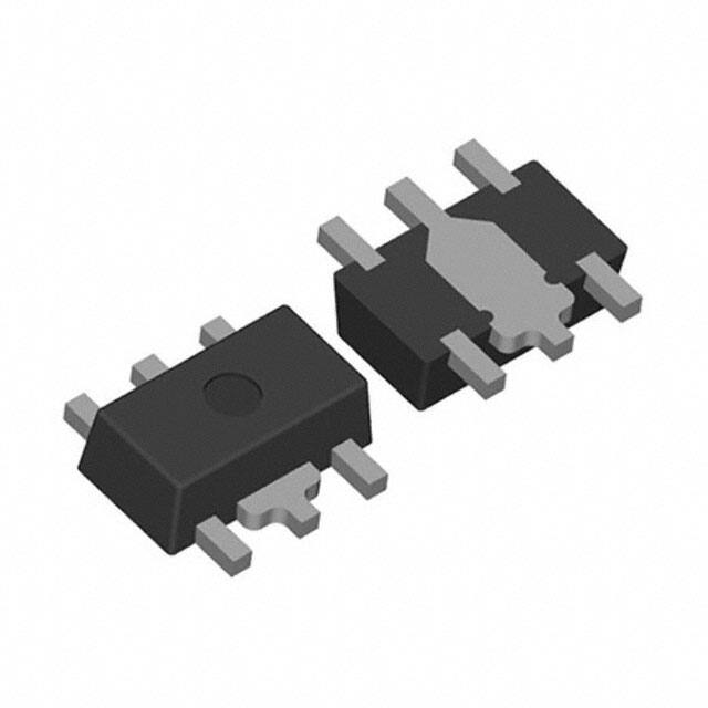
Since the packages for these ICs are the SOT-89-5 package, HSON-6, or HSOP-6J, high density mounting of
the ICs on boards is possible.
FEATURES
•
•
•
•
•
•
•
•
•
•
•
•
•
•
•
•
Output Current ............................................................. 1A
Supply Current ............................................................. Typ. 60μA
Standby Current ........................................................... Typ. 0.1μA
Input Voltage Range .................................................... 1.4V to 6.0V
Output Voltage Range.................................................. 0.8V to 5.0V (0.1V steps) (R1173xxx1)
1.0V to VIN (R1173x001)
(For other voltages, please refer to MARK INFORMATIONS.)
Dropout Voltage ........................................................... Typ. 0.32V (VOUT=1.5V, IOUT=1A)
Typ. 0.18V (VOUT=2.8V, IOUT=1A)
Ripple Rejection........................................................... Typ. 70dB (VOUT=2.8V)
Output Voltage Accuracy.............................................. ±2.0%
Temperature-drift Coefficient of Output Voltage........... Typ. ±100ppm/°C
Line Regulation ............................................................ Typ. 0.05%/V
Load Regulation........................................................... Typ. −2mV (IOUT=300mA)
Typ. −3mV (IOUT=1A)
Packages ..................................................................... SOT-89-5, HSON-6, HSOP-6J
Low inrush current at turning-on .................................. Typ. 500mA
Built-in Thermal Shutdown Circuit
Built-in Current Limit Circuit ......................................... Typ. 250mA
Output capacitors ......................................................... CIN=Ceramic 4.7μF
COUT=Tantalum 4.7μF (VOUT
= 1.0V)
APPLICATIONS
• Local Power source for Notebook PC.
• Local Power source for portable communication equipments, cameras, and videos.
• Local Power source for home appliances.
1
�R1173x
BLOCK DIAGRAMS
R1173xxx1B
VDD
R1173xxx1D
VOUT
VDD
Vref
VOUT
Vref
Current Limit
Current Limit
GND
CE
GND
CE
R1173x001B
VDD
R1173x001D
VOUT
VDD
VOUT
ADJ
ADJ
Vref
Vref
Current Limit
CE
2
Current Limit
GND
CE
GND
�R1173x
SELECTION GUIDE
The output voltage, auto discharge function, package for the ICs can be selected at the user’s request.
Product Name
Package
Quantity per Reel
Pb Free
Halogen Free
R1173Dxx1∗-TR-FE
HSON-6
3,000 pcs
Yes
Yes
R1173Hxx1∗-T1-FE
SOT-89-5
1,000 pcs
Yes
Yes
R1173Sxx1∗-E2-FE
HSOP-6J
1,000 pcs
Yes
Yes
xx : The output voltage can be designated in the range from 0.8V(08) to 5.0V(50) in 0.1V steps.
External Setting Type: 00 (ADJ pin voltage is fixed at 1.0V.)
(For other voltages, please refer to MARK INFORMATIONS.)
∗ : The auto discharge function at off state are options as follows.
(B) "H" active, without auto discharge function at off state
(D) "H" active, with auto discharge function at off state
3
�R1173x
PIN CONFIGURATIONS
z SOT-89-5
z HSON-6
Top View
5
z HSOP-6J
Bottom View
4
6
5
4
4
5
6
6
5
4
1
2
3
∗
∗
1
2
3
1
2
3
∗
3
2
1
PIN DESCRIPTIONS
zSOT-89-5
Pin No.
1
Symbol
Description
ADJ
ADJUST Pin (R1173H001x)
NC
No Connection (R1173Hxx1x)
2
GND
Ground Pin
3
CE
Chip Enable Pin ("H" Active)
4
VDD
Input Pin
5
VOUT
Output Pin
zHSON-6
Pin No.
Symbol
1
VOUT*1
Output Pin
2
1
Output Pin
3
VOUT*
Description
ADJ
ADJUST Pin (R1173D001x)
NC
No Connection (R1173Dxx1x)
4
GND
Ground Pin
5
CE
Chip Enable Pin ("H" Active)
6
VDD
Input Pin
∗) Tab and tab suspension leads in the
parts are GND level.
(They are connected to the reverse side of the IC.)
The tab is better to be connected to the GND, but leaving it open is also acceptable.
The tab suspension leads should be open and do not connect to other wires or land patterns.
∗1) The VOUT pin must be wired together when it is mounted on board.
4
�R1173x
zHSOP-6J
Pin No.
Symbol
1
VOUT
Output Pin
1
2
GND*
3
4
Description
Ground Pin
ADJ
ADJUST Pin (R1173S001x)
NC
No Connection (R1173Sxx1x)
CE
Chip Enable Pin ("H" Active)
1
5
GND*
6
VDD
Ground Pin
Input Pin
∗1) The GND pin must be wired together when it is mounted on board.
ABSOLUTE MAXIMUM RATINGS
Symbol
Item
VIN
Input Voltage
VCE
Input Voltage (CE Input Pin)
VOUT
Output Voltage
PD
Rating
Unit
6.5
V
−0.3 to 6.5
V
−0.3 to VIN+0.3
V
Power Dissipation (SOT-89-5)*
900
Power Dissipation (HSON-6)*
900
Power Dissipation (HSOP-6J)*
1700
mW
Topt
Operating Temperature
−40 to 85
°C
Tstg
Storage Temperature
−55 to 125
°C
∗) For Power Dissipation, please refer to PACKAGE INFORMATION.
ABSOLUTE MAXIMUM RATINGS
Electronic and mechanical stress momentarily exceeded absolute maximum ratings may cause the
permanent damages and may degrade the life time and safety for both device and system using the device
in the field.
The functional operation at or over these absolute maximum ratings is not assured.
RECOMMENDED OPERATING CONDITIONS (ELECTRICAL CHARACTERISTICS)
All of electronic equipment should be designed that the mounted semiconductor devices operate within the
recommended operating conditions. The semiconductor devices cannot operate normally over the
recommended operating conditions, even if when they are used over such conditions by momentary
electronic noise or surge. And the semiconductor devices may receive serious damage when they continue
to operate over the recommended operating conditions.
5
�R1173x
ELECTRICAL CHARACTERISTICS
•
R1173xxxxB/D (Fixed Output Voltage Type)
Symbol
Item
VIN
Input Voltage
ISS
Supply Current
Istandby Standby Current
VOUT
ΔVOUT/
ΔIOUT
Load regulation
VDIF
Dropout Voltage
ΔVOUT/
ΔVIN
Conditions
Min.
Typ. Max. Unit
1.4
6.0
V
VIN−VOUT=1.0V, VCE=VIN, IOUT=0A
60
100
μA
VIN= 6.0V, VCE=0V
0.1
1.0
μA
×0.98
×1.02
V
1.5V
−30
+30
mV
VIN−VOUT=0.3V, 1mA <
= IOUT <
= 300mA
1.1V,
then
V
IN
=1.4V
If VOUT <
=
−15
VIN−VOUT=1.0V
IOUT=100mA
VOUT>1.5V
VOUT
<
=
Refer to the following table
Ripple Rejection
f=1kHz (VOUT <
= 4.0V)
f=1kHz (VOUT>4.0V)
Ripple 0.5Vp-p,VIN−VOUT=1.0V, IOUT=100mA
If VOUT <
= 1.2V, VIN−VOUT=1.5V, IOUT=100mA
Output Voltage
Temperature Coefficient
IOUT=100mA,
−40°C <
= Topt
ILIM
Output Current
VIN−VOUT=1.0V
ISC
Short Current Limit
VOUT=0V
RPD
Pull-down resistance
for CE pin
1.9
VCEH
CE Input Voltage "H"
VCEL
CE Input Voltage "L"
TTSD
TTSR
en
<
=
0.05
0.20
70
60
85°C
ppm/
°C
1
A
250
MΩ
1.0
6.0
V
0
0.4
V
BW=10Hz to 100kHz
5.0
mA
15.0
Dropout Voltage by Output Voltage
150
°C
120
°C
30
μVrms
Topt=25°C
Dropout Voltage VDIF (V)
Output Voltage
VOUT (V)
6
IOUT=300mA
IOUT=1A
Typ.
Max.
Typ.
0.8
<
=
VOUT < 0.9
0.33
0.57
0.72
0.9
<
=
VOUT < 1.0
0.22
0.47
0.64
1.0
<
=
VOUT < 1.5
0.18
0.32
0.56
1.5
<
=
VOUT < 2.6
0.10
0.15
0.32
0.05
0.10
0.18
2.6
<
=
VOUT
%/V
dB
±100
Thermal Shutdown Detector
Junction Temperature
Threshold Temperature
Thermal Shutdown
Junction Temperature
Released Temperature
Output Noise
15
−3
IOUT=100mA, VOUT+0.5V <
= VIN <
= 6.0V
<
<
0.9V,
1.4V
V
IN
If VOUT <
=
=
= 6.0V
ΔVOUT/
ΔTopt
−2
mV
VIN−VOUT=0.3V, 1mA <
= IOUT <
= 1A
1.1V,
then
V
IN
=1.7V
If VOUT <
=
Line regulation
RR
•
Output voltage
Topt=25°C
�R1173x
•
R1173x001B/D (Adjustable Output Voltage Type)
Symbol
Item
Topt=25°C
Conditions
Min.
Typ.
Unit
6.0
V
VIN
Input Voltage
ISS
Supply Current
VOUT=VADJ, VIN=2.0, VCE=VIN
60
100
μA
Standby Current
VIN=6.0V, VCE=0V
0.1
1.0
μA
Reference Voltage for
Adjustable Voltage Regulator
VOUT=VADJ, VIN=2.0V
IOUT=100mA
1.000
1.030
V
VIN
V
Istandby
VOUT
RVOUT
ΔVOUT/
ΔIOUT
1.4
Max.
Output Voltage Range
Load regulation
0.970
1.0
VIN=1.4V
1mA <
= IOUT
<
=
300mA
VIN=1.7V
1mA <
= IOUT
<
=
1A
−15
−2
15
mV
−3
IOUT=300mA
0.18
IOUT=1A
0.56
Line regulation
VOUT=VADJ, IOUT=100mA
1.5V <
= VIN <
= 6.0V
0.05
Ripple Rejection
f=1kHz Ripple 0.5Vp−p,
VOUT=VADJ, VIN=2.5V
IOUT=100mA
70
dB
Output Voltage
Temperature Coefficient
IOUT=100mA
−40°C <
= Topt
±100
ppm/°C
ILIM
Output Current
VOUT=VADJ, VIN=2.0
ISC
Short Current Limit
VOUT=VADJ=0V
RPD
Pull-down resistance for CE pin
VDIF
ΔVOUT/
ΔVIN
RR
ΔVOUT/
ΔTopt
Dropout Voltage
VOUT=VADJ
<
=
85°C
0.32
0.20
1
%/V
A
250
1.9
V
5.0
mA
15.0
MΩ
VCEH
CE Input Voltage "H"
1.0
6.0
V
VCEL
CE Input Voltage "L"
0
0.4
V
TTSD
TTSR
en
Thermal Shutdown Detector
Threshold Temperature
Thermal Shutdown
Released Temperature
Output Noise
Junction Temperature
150
°C
Junction Temperature
120
°C
BW=10Hz to 100kHz
30
μVrms
7
�R1173x
Technical Notes on External Components and Typical Application
(Refer to the example of typical application)
VIN
VDD
VOUT
GND
ADJ
C1
C2
R1173xxx
Series
IOUT
VOUT
V
CE
Example of the typical application of R1173x (Fixed Output Type)
Phase Compensation
In these ICs, phase compensation is made with the output capacitor for securing stable operation even if the
load current is varied. For this purpose, use as much as a capacitor as C2. Recommendation value is as follows:
Mounting on PCB
Make VDD and GND lines sufficient. If their impedance is high, a current flows, the noise picked up or unstable
operation may result. Further use a 4.7μF or more value capacitor between VDD pin and GND pin as close as
possible.
Set an Output capacitor between VOUT pin and GND pin for phase compensation as close as possible.
Output Voltage
C2 recommendation value
VOUT


 工商网监
湘ICP备2023018690号
工商网监
湘ICP备2023018690号