R1191x SERIES
300mA LDO REGULATOR with the Reverse Current Protection
NO.EA-229-111026
OUTLINE
R1191x Series are a low supply current voltage regulator with high output voltage accuracy. The maximum
operating voltage is 16V. These ICs can switch to the fast mode and the low power mode by the low power / fast
mode changer pin (ECO pin) without changing the output voltage value.
Each of these ICs consists of a voltage reference unit, an error amplifier, a resistor-net for voltage setting, a
short current limit circuit, a thermal shutdown circuit and a chip enable circuit.
Moreover, the R1191x Series has the reverse current protection function, which protects the reverse current
flow into VDD pin when the output pin voltage becomes higher than the VDD pin voltage. Thus it is suitable for the
back-up circuit.
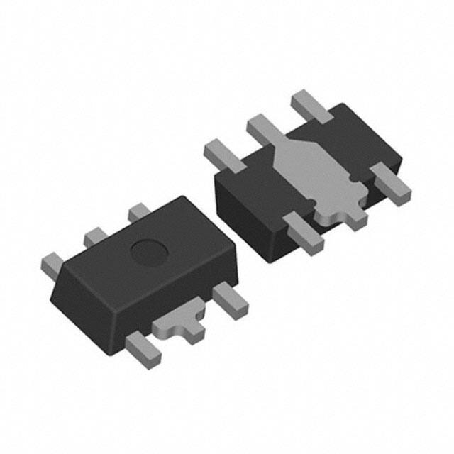
Since the packages for these ICs are SOT-89-5, SOT-23-5 and DFN1616-6, therefore high density mounting
of the ICs on boards is possible.
FEATURES
• Supply Current ..................................................... Typ. 50μA (Fast Mode),
Typ. 6.0μA (Low Power Mode)
• Standby Mode ...................................................... Typ. 0.3μA
• Reverse Current................................................... Max. 0.1μA
• Output Current ..................................................... Min. 300mA
• Input Voltage Range ............................................ 3.5V to 16.0V
• Output Voltage Range.......................................... 2.0V to 15.0V (0.1V steps)
(For other voltages, please refer to MARK INFORMATIONS.)
• Output Voltage Accuracy...................................... ±1.5% (Fast Mode)
±2.5% (Low Power Mode)
• Temperature-Drift Coefficient of Output Voltage .. Typ. ±80ppm/°C
• Dropout Voltage ................................................... Typ. 0.55V (Fast Mode, IOUT=300mA ,VOUT=5.0V)
Typ. 0.70V (Low Power Mode, IOUT=300mA,VOUT=5.0V)
• Ripple Rejection................................................... Typ. 60dB (f=1kHz,VOUT=5.0V, Fast Mode)
• Line Regulation .................................................... Typ. 0.02%/V (Fast Mode)
• Packages ............................................................ DFN1616-6, SOT-23-5, SOT-89-5
• Built-in fold-back protection circuit ....................... Typ. 50mA (Current at short mode)
• Built-in Thermal Shutdown Circuit........................ Shutdown Temperature at 150°C
• Ceramic capacitors are recommended to be used with this IC ····CIN=2.2μF or more, COUT=4.7μF or more
APPLICATIONS
• Power source for digital home appliances
• Power source for audio visual equipment
1
�R1191x
BLOCK DIAGRAM
R1191xxxxB
R1191xxxxD
ECO
ECO
Thermal Shutdown
VDD
Thermal Shutdown
VOUT
VDD
VOUT
Vref
Vref
Peak
Short
Current
Protection Protection
Peak
Short
Current
Protection Protection
Reverse
Detector
CE
Reverse
Detector
GND CE
GND
SELECTION GUIDE
The output voltage, auto-discharge function, and package, for the ICs can be selected at the user’s request.
Product Name
Package
Quantity per Reel
Pb Free
Halogen Free
DFN1616-6
5,000 pcs
Yes
Yes
R1191Nxxx∗-TR-FE
SOT-23-5
3,000 pcs
Yes
Yes
R1191Hxxx∗-T1-FE
SOT-89-5
1,000 pcs
Yes
Yes
R1191Lxxx∗-TR
xxx : The output voltage can be designated in the range from 2.0V(020) to 15.0V(150) in 0.1V steps.
(For other voltages, please refer to MARK INFORMATIONS.)
∗ : The auto discharge function at off state are options as follows.
(B) without auto discharge function at off state.
(D) with auto discharge function at off state.
2
�R1191x
PIN CONFIGURATIONS
• DFN1616-6*1
Top View
6
5
4
• SOT-23-5
Bottom View
4
5
2
3
3
2
4
5
3
1
4
6
∗
1
5
• SOT-89-5
(mark side)
1
1
2
2
3
PIN DISCRIPTIONS
•
DFN1616-6*1
Pin No
Symbol
Pin Description
1
ECO
2
NC
No Connection
3
VDD
Input Pin
4
VOUT
Output pin
5
GND
Ground Pin
6
CE
Low Power / Fast Mode Changer Pin ("H": Fast Mode)
Chip Enable Pin ("H" Active)
∗1) Tab is GND level. (They are connected to the reverse side of this IC.)
The tab is better to be connected to the GND, but leaving it open is also acceptable.
•
•
SOT-23-5
Pin No
Symbol
Pin Description
1
ECO
Low Power / Fast Mode Changer Pin ("H": Fast Mode)
2
GND
Ground Pin
3
CE
Chip Enable Pin ("H" Active)
4
VOUT
Output pin
5
VDD
Input Pin
SOT-89-5
Pin No
Symbol
Pin Description
1
VOUT
Output pin
2
GND
Ground Pin
3
CE
4
ECO
5
VDD
Chip Enable Pin ("H" Active)
Low Power / Fast Mode Changer Pin ("H": Fast Mode)
Input Pin
3
�R1191x
ABSOLUTE MAXIMUM RATINGS
Symbol
Item
Rating
Unit
VIN
Input Voltage
−0.3 to 18.0
V
VCE
Input Voltage (CE Pin)
−0.3 to 18.0
V
VECO
Input Voltage (ECO Pin)
−0.3 to VIN + 0.3 ≤ 18.0
V
VOUT
Output Voltage
−0.3 to 18.0
V
IOUT
Output Current
400
mA
Power Dissipation (DFN1616-6)*
640
Power Dissipation (SOT-23-5)*
420
Power Dissipation (SOT-89-5)*
900
Topt
Operating Temperature Range
−40 to +85
°C
Tstg
Storage Temperature Range
−55 to +125
°C
PD
mW
∗) For Power Dissipation, please refer to PACKAGE INFORMATION.
ABSOLUTE MAXIMUM RATINGS
Electronic and mechanical stress momentarily exceeded absolute maximum ratings may cause the
permanent damages and may degrade the life time and safety for both device and system using the device
in the field.
The functional operation at or over these absolute maximum ratings is not assured.
RECOMMENDED OPERATING CONDITIONS (ELECTRICAL CHARACTERISTICS)
All of electronic equipment should be designed that the mounted semiconductor devices operate within the
recommended operating conditions. The semiconductor devices cannot operate normally over the
recommended operating conditions, even if when they are used over such conditions by momentary
electronic noise or surge. And the semiconductor devices may receive serious damage when they continue
to operate over the recommended operating conditions.
4
�R1191x
ELECTRICAL CHARACTERISTICS
VIN=VCE=Set VOUT+3.0V (Max.16V), CIN=2.2μF, COUT=4.7μF IOUT=1mA, unless otherwise noted.
are applicable under the condition of −40°C ≤ Topt ≤ 85°C.
The values in
Topt=25°C
R1191xxxxB/D
Symbol
Item
Conditions
Fast Mode VECO=VIN
VOUT
ΔVOUT
IOUT
Output Voltage
Low Power
VECO=0V
Mode
Min.
Typ.
Max.
Topt=25°C
−40°C ≤ Topt ≤ 85°C
Topt=25°C
×0.985
×0.970
×0.975
×1.015
×1.030
×1.025
−40°C ≤ Topt ≤ 85°C
×0.960
×1.040
Output Voltage Deviation between Fast Mode and Low Power Mode
−1.5
0
1.5
Output Current
300
VECO=VIN,
Fast Mode
50
1mA ≤ IOUT ≤ 300mA
ΔVOUT/
Load Regulation
ΔIOUT
Low Power VECO=GND,
60
Mode
1mA ≤ IOUT ≤ 300mA
VDIF
Dropout Voltage
Refer to the following table
Unit
V
%
mA
120
mV
130
ISS1
Supply Current (Fast Mode) VECO=VIN, IOUT=0mA
50
100
μA
ISS2
Supply Current
(Low Power Mode)
6
15
μA
VECO=GND, IOUT=0mA
Istandby Supply Current (Standby)
VIN=16V, VCE=0V
(If VOUT < 3.0V, VIN=14V)
0.3
1.0
μA
ΔVOUT/
Line Regulation
ΔVIN
Set VOUT+0.5V ≤ VIN ≤ 16V
(If Set VOUT < 3.0V, 3.5V ≤ VIN ≤ 14V)
0.02
0.10
%/V
RR
VIN
ΔVOUT/
ΔTopt
ISC
VCEH
VCEL
TTSD
TTSR
RLOW
IREV
Ripple Rejection
Input Voltage
f=1kHz, IOUT=30mA 2.0V≤VOUT
很抱歉,暂时无法提供与“R1191H030B-T1-FE”相匹配的价格&库存,您可以联系我们找货
免费人工找货