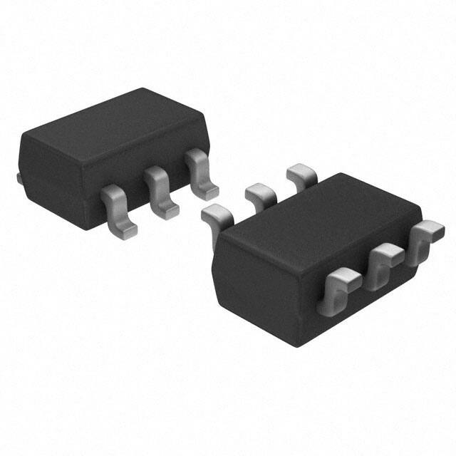
*R1203L(DFN1616-6B) is the non-promotional product of as February 2021.
R1203x SERIES
STEP-UP DC/DC CONVERTER FOR WHITE LED BACK LIGHT
NO.EA-271-180703
OUTLINE
The R1203x Series are PWM control type step-up DC/DC converter ICs with low supply current.
The R1203x is fully dedicated to drive White LEDs with constant current. Each of these ICs consists of an
NMOS FET, an oscillator, a PWM comparator, a voltage reference unit, an error amplifier, a current limit circuit,
an under voltage lockout circuit (UVLO), and an over-voltage protection circuit (OVP).
The R1203x can drive white LEDs in constant current with high efficiency by using an inductor, a diode, a
resistor and capacitors as external components.
The LEDs current can be set by an external resistance value and can adjust the dimming of LEDs by CE pin
according to the signal of PWM. Feedback voltage is 0.2V, therefore power loss by current setting resistance is
small and efficiency is good. Maximum duty cycle is internally fixed, Typ. 91%. LEDs can be driven from low
voltage. Protection circuits are the current limit of Lx peak current, the over voltage limit of output, and the under
voltage lockout function.
It is controllable the dimming of LEDs quickly when the PWM signal (between 200Hz to 300kHz) input to CE
pin. If the CE pin input is "L" in the fixed time (Typ. 0.5ms), the IC becomes the standby mode and turns OFF
LEDs.
FEATURES
•
•
•
•
•
•
•
•
•
•
•
•
•
•
•
•
Supply Current ....................................................... Typ. 500µA
Standby Current ..................................................... Max. 5µA
Input Voltage Range ............................................... 1.8V to 5.5V
Feedback Voltage .................................................. 0.2V
Feedback Voltage Accuracy ................................... ±1.0% (±10mV)
Temperature-Drift Coefficient of Feedback Voltage ... ±150ppm/°C
Oscillator Frequency............................................... Typ. 1.2MHz
Maximum Duty Cycle ............................................. Typ. 91%
Switch ON Resistance............................................ Typ. 1.35Ω
UVLO Detector Threshold ....................................... Typ. 1.6V
Lx Current Limit Protection ..................................... Typ. 700mA
OVP Detector Threshold ......................................... Typ. 29.5V
Switching Control ................................................... PWM
LED dimming control .............................................. by external PWM signal (Frequency 200Hz to 300kHz )
Packages .............................................................. DFN1616-6B, SOT-23-6
Ceramic capacitors are recommended ..................... 0.22µF
APPLICATION
• White LED Backlight for portable equipment
1
�*R1203L(DFN1616-6B) is the non-promotional product of as February 2021.
R1203x
NO.EA-271-180703
SELECTION GUIDE
The package for the ICs can be selected at the user's request.
Product Name
R1203L071B-TR
Package
Quantity per Reel
Pb Free
Halogen Free
DFN1616-6B
5,000 pcs
Yes
Yes
SOT-23-6
3,000 pcs
Yes
Yes
R1203N071B-TR-FE
BLOCK DIAGRAMS
VFB
VIN
LX
VOUT
UVLO
Err. Amp.
PWM Comp.
+
+
–
–
R
Q
S
Switch
Control
OVP
vref
Oscillator
PWM
Cntrl
EN
Shutdown
delay
Slope Compensation
Current
Protect
Current
sense
Σ
CE
CE
2
GND
�*R1203L(DFN1616-6B) is the non-promotional product of as February 2021.
R1203x
NO.EA-271-180703
PIN DESCRIPTIONS
• DFN1616-6B
Top View
6
5
• SOT-23-6
Bottom View
4
4
5
6
•
2
3
3
2
4
6
∗
1
5
(mark side)
1
1
2
3
DFN1616-6B
Pin No
Symbol
Pin Description
1
CE
Chip Enable Pin ("H" Active)
2
VFB
Feedback Pin
3
Lx
Switching Pin (Open Drain Output)
4
GND
5
VIN
6
VOUT
Ground Pin
Input Pin
Output Pin
∗) Tab is GND level. (They are connected to the reverse side of this IC.)
The tab is better to be connected to the GND, but leaving it open is also acceptable.
•
SOT-23-6
Pin No
Symbol
Pin Description
1
CE
2
VOUT
3
VIN
Input Pin
4
Lx
Switching Pin (Open Drain Output)
5
GND
6
VFB
Chip Enable Pin ("H" Active)
Output Pin
Ground Pin
Feedback Pin
3
�*R1203L(DFN1616-6B) is the non-promotional product of as February 2021.
R1203x
NO.EA-271-180703
ABSOLUTE MAXIMUM RATINGS
Symbol
(GND=0V)
Item
Rating
Unit
VIN
VIN Pin Voltage
−0.3 to 6.5
V
VCE
CE Pin Voltage
−0.3 to VIN+0.3
V
VFB
VFB Pin Voltage
−0.3 to VIN+0.3
V
VOUT
VOUT Pin Voltage
−0.3 to 32
V
VLX
LX Pin Voltage
−0.3 to 32
V
ILX
LX Pin Current
1000
mA
PD
Power Dissipation ∗
(JEDEC STD. 51-7 Test Land Pattern)
Tj
Junction Temperature Range
−40 to 125
°C
Tstg
Storage Temperature Range
−55 to 125
°C
DFN1616-6B
SOT-23-6
2400
660
mW
∗) Refer to POWER DISSIPATION for detailed information.
ABSOLUTE MAXIMUM RATINGS
Electronic and mechanical stress momentarily exceeded absolute maximum ratings may cause the permanent damages
and may degrade the life time and safety for both device and system using the device in the field. The functional
operation at or over these absolute maximum ratings is not assured.
RECOMMENDED OPERATING CONDITIONS
Symbol
Item
Rating
Unit
VIN
Input Voltage
1.8 to 5.5
V
Ta
Operating Temperature Range
−40 to 85
°C
RECOMMENDED OPERATING CONDITIONS
All of electronic equipment should be designed that the mounted semiconductor devices operate within the
recommended operating conditions. The semiconductor devices cannot operate normally over the recommended
operating conditions, even if when they are used over such ratings by momentary electronic noise or surge. And the
semiconductor devices may receive serious damage when they continue to operate over the recommended operating
conditions.
4
�*R1203L(DFN1616-6B) is the non-promotional product of as February 2021.
R1203x
NO.EA-271-180703
ELECTRICAL CHARACTERISTICS
•
R1203x
Symbol
IDD
Istandby
(Ta=25°C)
Item
Conditions
Min.
Unit
VIN=5.5V, VFB =0V, Lx at no load
0.5
1.0
mA
Standby Current
VIN=5.5V, VCE=0V
1.0
5.0
µA
1.6
1.7
V
VUVLO1
+0.1
1.8
V
UVLO Detector Threshold VIN falling
VUVLO2
UVLO Released Voltage
VIN rising
VCEH
CE Input Voltage "H"
VIN=5.5V
VCEL
CE Input Voltage "L"
VIN=1.8V
RCE
CE Pull Down Resistance VIN=3.6V
600
VFB
VFB Voltage Accuracy
VIN=VCE=3.6V
0.19
VFB Voltage Temperature
Coefficient
VIN=VCE=3.6V, -40°C ≤ Ta ≤ 85°C
VFB Input Current
VIN=5.5V, VFB=0V or VIN
RON
Switch ON Resistance
VIN=3.6V, ILX=100mA
ILXleak
Switch Leakage Current
VLX=30V
ILXlim
Switch Current Limit
VIN=3.6V
fosc
Oscillator Frequency
IFB
Max.
Supply Current
VUVLO1
∆VFB/
∆Ta
Typ.
Maxduty Maximum Duty Cycle
1.5
1.5
V
0.5
V
1200
2200
kΩ
0.20
0.21
V
ppm
/°C
±150
−0.1
0.1
µA
Ω
1.35
0
3.0
µA
400
700
1000
mA
VIN=3.6V, VOUT=VFB=0V
1.0
1.2
1.4
MHz
VIN=3.6V, VOUT=VFB=0V
86
91
28.7
29.5
%
VOVP1
OVP Detector Threshold
VIN=3.6V, VOUT rising
30.3
V
∆VOVP1/
∆Ta
VOVP1 Voltage
Temperature Coefficient
VIN=VCE=3.6V, −40°C ≤ Ta ≤ 85°C
±150
ppm
/°C
VOVP2
OVP Released Voltage
VIN=3.6V, VOUT falling
VOVP1
−1.55
V
5
�*R1203L(DFN1616-6B) is the non-promotional product of as February 2021.
R1203x
NO.EA-271-180703
THEORY OF OPERATION
Operation of Step-Up DC/DC Converter and Output Current
i2
IOUT
VOUT
Diode
L
VIN
i1
Lx Tr
CL
GND
Di scontinuous mode
Continuous mode
ILmax
IL
IL
ILmax
ILmin
ILmin
topen
t
toff
ton
T=1/fosc
t
ton
toff
T=1/fosc
There are two operation modes of the step-up PWM control-DC/DC converter. That is the continuous mode and
discontinuous mode by the continuousness inductor.
When the transistor turns ON, the voltage of inductor L becomes equal to VIN voltage. The increase value of
inductor current (i1) will be
∆i1 = VIN × ton / L................................................................................................... Formula 1
As the step-up circuit, during the OFF time (when the transistor turns OFF) the voltage is continually supply from
the power supply. The decrease value of inductor current (i2) will be
∆i2 = (VOUT − VIN) × t open / L ................................................................................... Formula 2
6
�*R1203L(DFN1616-6B) is the non-promotional product of as February 2021.
R1203x
NO.EA-271-180703
At the PWM control-method, the inductor current become continuously when t open=t off , the DC/DC convert er
operate as the continuous mode.
In the continuous mode, the variation of current of i1 and i2 is same at regular condition.
VIN × ton / L = (VOUT - VIN) × t off / L ............................................................................Formula 3
The duty at continuous mode will be
duty (%)= ton / (ton + toff ) = (VOUT - VIN) / VOUT............................................................Formula 4
The average of inductor current at tf = t off will be
IL(A ve.) = VIN × ton / (2 × L).....................................................................................Formula 5
If the input voltage = output voltage, the IOUT will be
IOUT = VIN2 × ton / (2 × L × VOUT)................................................................................Formula 6
If the IOUT value is large than above the calculated value (Formula 6), it will become the continuous mode, at this
status, the peak current (ILmax ) of inductor will be
IL max = IOUT × VOUT / VIN + VIN × ton / (2 × L) ..............................................................Formula 7
IL max = IOUT × VOUT / VIN + VIN × T × (VOUT - VIN) / (2 × L × VOUT)...................................Formula 8
The peak current value is larger than the IOUT value. In case of this, selecting the condition of the input and the
output and the external components by considering of ILmax value.
The explanation above is based on the ideal calculation, and the loss caused by LX switch and the external
components are not included.
The actual maximum output current will be between 50% and 80% by the above calculations. Especially, when
the IL is large or VIN is low, the loss of VIN is generated with on resistance of the switch. Moreover, it is necessary
to consider Vf of the diode (approximately 0.8V) about V OUT.
•
Soft-Start
The output of the error amplifier starts from 0V and the inrush current is suppressed when starting by the CE pin
"H" input. Moreover, the inrush current can be suppressed by gradually enlarging Duty of the PWM signal to the
CE pin.
7
�*R1203L(DFN1616-6B) is the non-promotional product of as February 2021.
R1203x
NO.EA-271-180703
APPLICATION INFORMATION
•
Typical Applications
L1
22µH
C1
1µF
C2
0.22µF
VIN
LX
CE
VOUT
GND
•
VFB
R1
10Ω
Selection of Inductors
The peak current of the inductor at normal mode can be estimated as the next formula when the efficiency is 80%.
ILmax =1.25 x IOUT x VOUT / VIN + 0.5 x VIN x (VOUT - VIN) / (L x VOUT x fosc )
In the case of start-up or dimming control by CE pin, inductor transient current flows, and the peak current of it
must be equal or less than the current limit of the IC. The peak current should not beyond the rated current of the
inductor. The recommended inductance value is 10-22µH.
Table 1 Peak current value in each condition
VIN (V)
3
3
3
3
Condition
VOUT (V) IOUT (mA)
14
20
14
20
21
20
21
20
L (µH)
10
22
10
22
ILmax (mA)
215
160
280
225
Table 2 Recommended inductors
L
(µH)
10
10
10
10
22
22
22
8
Part No.
LQH32CN100K53
LQH2MC100K02
VLF3010A-100
VLS252010-100
LQH32CN220K53
LQH2MC220K02
VLF3010A-220
Rated
Current (mA)
450
225
490
520
250
185
330
Size
(mm)
3.2x2.5x1.55
2.0x1.6x0.9
2.8x2.6x0.9
2.5x2.0x1.0
3.2x2.5x1.55
2.0x1.6x0.9
2.8x2.6x0.9
�*R1203L(DFN1616-6B) is the non-promotional product of as February 2021.
R1203x
NO.EA-271-180703
•
Selection of Capacitors
Set 1µF or more value bypass capacitor C1 between VIN pin and GND pin as close as possible.
Set 0.22µF or more capacitor C2 between VOUT and GND pin.
Note the VOUT that depends on LED used, and select the rating of V OUT or more.
•
Selection of SBD (Schottky Barrier Diode)
Select the diode with low VF such as Schottky type with low reverse current IR, and with low capacitance.
Table 3 Recommended components
Rated voltage (V)
Part No.
6.3
25
50
30
30
CM105B105K06
GRM21BR11E224
GRM21BR71H224
CRS10I30A
RSX051VA-30
C1
C2
D1
•
LED Current Setting
When CE pin input is "H" (Duty=100%), LED current can be set with feedback resistor (R1)
ILED=VFB / R1
•
LED Dimming Control
The LED brightness can be controlled by inputting the PWM signal to the CE pin. If the CE pin input is "L" in the
fixed time (Typ.0.5ms), the IC becomes the standby mode and turns OFF LEDs.
The current of LEDs when the CE pin is "H" input (Duty=100%) is shown by the above expression. The current
of LEDs can be controlled by Duty of the PWM signal of the input CE pin. The current of LEDs when High-Dut y
of the CE input is Hduty reaches the value as calculatable following formula.
ILED=Hduty × VFB / R1
The frequency of the PWM signal is using the range between 200Hz to 300kHz.
When controlling the LED brightness by the PWM signal of 20kHz or less; The increasing or decreasing of the
inductor current might be make a sounds in the hearable sound wave area. In that case, please use the PWM
signal in the high frequency area.
CE
Hduty
VFB
R1
Dimming control by CE pin input
9
�*R1203L(DFN1616-6B) is the non-promotional product of as February 2021.
R1203x
NO.EA-271-180703
TECHNICAL NOTES
Current Path on PCB
The current paths in an application circuit are shown in Fig. 1 and 2.
A current flows through the paths shown in Fig. 1 at the time of MOSFET-ON, and shown in Fig. 2 at the time of
MOSFET-OFF. In the paths pointed with red arrows in Fig. 2, current flows just in MOSFET-ON period or just in
MOSFET-OFF period. Parasitic impedance/inductance and the capacitance of these paths influence stability of
the system and cause noise outbreak. So please minimize this side effect. In addition, please shorten the wiring
of other current paths shown in Fig. 1 and 2 except for the paths of LED load.
Layout Guide for PCB
⋅
⋅
⋅
⋅
Please shorten the wiring of the input capacitor (C1) between V IN pin and GND pin of IC. The GND pin should
be connected to the strong GND plane.
The area of LX land pattern should be smaller.
The wiring between LX pin and inductor and diode should be short and please put output capacitor (C2) close
to the cathode of diode.
Please make the GND side of output capacitor (C2) close to the GND pin of IC.
⋅
10
MOSFET-ON
Load
Load
Fig. 1
Fig. 2
MOSFET-OFF
�*R1203L(DFN1616-6B) is the non-promotional product of as February 2021.
R1203x
NO.EA-271-180703
PCB Layout
・ PKG: DFN1616-6B pin
R1203L Typical Board Layout
Top Layer
Back Layer
・ PKG: SOT-23-6pin
R1203N Typical Board Layout
Top Layer
Back Layer
U1-● indicates the position of No.1 pin.
11
�*R1203L(DFN1616-6B) is the non-promotional product of as February 2021.
R1203x
NO.EA-271-180703
TYPICAL CHARACTERISTICS
1) Efficiency vs. Output Current Characteristics
7LEDs
90
90
85
85
80
80
Efficiency (%)
Efficiency (%)
6LEDs
75
70
65
VIN=2.8V
VIN =2.8V
VIN=2.8V
VIN =3.6V
VIN=3.6V
VIN=3.6V
V
IN =5.0V
VIN=5.0V
VIN=5.0V
60
55
75
70
65
V
VIN=2.8V
IN =2.8V
60
V
IN =3.6V
VIN=3.6V
55
V
IN =5.0V
VIN=5.0V
50
50
0
5
10
15
0
20
5
10
15
20
Output Current IOUT (mA)
Output Current IOUT (mA)
2) PWM Dimming Duty Cycle vs. Output Current (R1=10Ω)
Output Current I OUT (mA)
25
Freq=200Hz
20
Freq=10kHz
Freq=300kHz
15
10
5
0
0
20
40
60
80
100
PWM Dimming Duty Cycle (%)
3) Output Current Ripple during PWM Dimming
f=200Hz
25
0.5
20
0.3
15
VFB
0.2
10
CE
0.1
5
30
25
VOUT
0.4
20
0.3
15
0.2
10
VFB
0.1
5
CE
0
0
-2
0
2
4
6
8
10 12 14 16
Time t (ms)
12
0
-0.04
0
0.04
0.12
0.20
Time t (ms)
0.28
V OUT/CE Voltage (V)
V FB Voltage (V)
0.4
0.6
V FB Voltage (V)
VOUT
0.5
30
V OUT/CE Voltage (V)
0.6
f=10kHz
�*R1203L(DFN1616-6B) is the non-promotional product of as February 2021.
R1203x
NO.EA-271-180703
f=300kHz
30
V FB Voltage (V)
0.5
25
VOUT
0.4
20
0.3
15
0.2
10
VFB
0.1
5
V OUT/CE Voltage (V)
0.6
CE
0
0
-2
0
2
4
6
8
10 12 14 16
Time t (µs)
4) VFB Voltage vs. Temperature
5) Supply Current vs. Temperature
800
0.205
Supply Current IDD (µA)
0.204
V FB Voltage (V)
0.203
0.202
0.201
0.200
0.199
0.198
0.197
700
600
500
0.196
0.195
400
-50
-25
0
25
50
75
100
-50
-25
Temparature Ta (°C)
25
50
75
100
75
100
Temparature Ta (°C)
6) Oscillator Frequency vs. Temperature
7) Maxduty vs. Temperature
94
1250
93
1225
Maxduty (%)
Frequency fosc (kHz)
0
1200
92
91
90
1175
89
1150
88
-50
-25
0
25
50
Temparature Ta (°C)
75
100
-50
-25
0
25
50
Temparature Ta (°C)
13
�*R1203L(DFN1616-6B) is the non-promotional product of as February 2021.
R1203x
NO.EA-271-180703
8) UVLO Output Voltage vs. Temperature
9) OVP Voltage vs. Temperature
1.80
30.5
30
29.5
OVP Voltage [V]
UVLO Voltage (V)
1.75
1.70
UVLO Released Voltage
1.65
1.60
UVLO Detector Voltage
29
OVP Detector Voltage
28.5
28
27.5
1.55
OVP Released Voltage
27
1.50
-50
-25
0
25
50
75
26.5
-50
100
-25
50
75
100
1.6
1000
1.4
900
VIN =2.5V
VIN=2.5V
800
VIN =3.6V
VIN=3.6V
VIN =1.8V
VIN=1.8V
1.2
1.0
0.8
0.6
0.4
0.2
0.0
VIN =5.5V
VIN=5.5V
700
600
500
400
300
200
-50
-25
0
25
50
75
100
Temparature Ta (°C)
34
32
30
28
26
20
22
24
26
28
30
32
Time t (ms)
34
36
-50
-25
0
25
50
Temparature Ta (°C)
12) OVP Operating Output Voltage Waveform
Output Voltage V OUT (V)
25
11) LX Current Limit vs. Temperature
Lx Limit Current I LIM (mA)
Switch ON Resistance R ON (Ω)
10) Switch ON Resistance vs. Temperature
14
0
Tempareture (°C)
Temparature Ta (°C)
38
40
75
100
�*R1203L(DFN1616-6B) is the non-promotional product of as February 2021.
POWER DISSIPATION
DFN1616-6B
Ver. A
The power dissipation of the package is dependent on PCB material, layout, and environmental conditions.
The following conditions are used in this measurement.
Measurement Conditions
Item
Measurement Conditions (JEDEC STD. 51-7)
Environment
Mounting on Board (Wind Velocity = 0 m/s)
Board Material
Glass Cloth Epoxy Plastic (Four-Layer Board)
Board Dimensions
76.2 mm × 114.3 mm × 0.8 mm
Copper Ratio
1st Layer: Less than 95% of 50 mm Square
2nd, 3rd, 4th Layers: Approx. 100% of 50 mm Square
Through-holes
φ 0.2 mm × 15 pcs
Measurement Result
(Ta = 25°C, Tjmax = 125°C)
Item
Measurement Result
Power Dissipation
2400 mW
Thermal Resistance (θja)
θja = 41°C/W
Thermal Characterization Parameter (ψjt)
ψjt = 11°C/W
θja: Junction-to–ambient thermal resistance.
ψjt: Junction–to-top of package thermal characterization parameter.
2500
2400
Power Dissipation PD (mW)
2000
1500
1000
500
0
0
25
50
75 85
100
125
Ambient Temperature (°C)
Power Dissipation vs. Ambient Temperature
Measurement Board Pattern
i
�*R1203L(DFN1616-6B) is the non-promotional product of as February 2021.
PACKAGE DIMENSIONS
DFN1616-6B
Ver. A
1.30±0.05
(3X0.15)
B
0.70±0.05
X4
1.60
0.05
4
6
∗
0.25±0.05
1.60
A
INDEX
0.4max.
0.1±0.05
3
0.5
0.20±0.05
1
0.05 M AB
Bottom View
S
0.05 S
DFN1616-6B Package Dimensions (Unit: mm)
*
∗ The tab on the bottom of the package shown by blue circle is a substrate potential (GND). It is recommended that this
tab be connected to the ground plane pin on the board but it is possible to leave the tab floating.
i
�*R1203L(DFN1616-6B) is the non-promotional product of as February 2021.
POWER DISSIPATION
SOT-23-6
Ver. A
The power dissipation of the package is dependent on PCB material, layout, and environmental conditions.
The following conditions are used in this measurement.
Measurement Conditions
Item
Measurement Conditions (JEDEC STD. 51-7)
Environment
Mounting on Board (Wind Velocity = 0 m/s)
Board Material
Glass Cloth Epoxy Plastic (Four-Layer Board)
Board Dimensions
76.2 mm × 114.3 mm × 0.8 mm
Copper Ratio
1st Layer : Less than 95% of 50 mm Square
2nd, 3rd, 4th Layers: Approx. 100% of 50 mm Square
Through-holes
φ 0.3 mm × 7 pcs
Measurement Result
(Ta = 25°C, Tjmax = 125°C)
Item
Measurement Result
Power Dissipation
660 mW
Thermal Resistance (θja)
θja = 150°C/W
Thermal Characterization Parameter (ψjt)
ψjt = 51°C/W
θja: Junction-to–ambient thermal resistance.
ψjt: Junction–to-top of package thermal characterization parameter
700
660
Power Dissipation PD (mW)
600
500
400
300
200
100
0
0
25
50
75 85
100
125
Ambient Temperature (°C)
Power Dissipation vs. Ambient Temperature
Measurement Board Pattern
i
�*R1203L(DFN1616-6B) is the non-promotional product of as February 2021.
PACKAGE DIMENSIONS
SOT-23-6
Ver. A
2.9±0.2
+0.2
1.1-0.1
1.9±0.2
4
1
2
0 to 0.1
0.2MIN.
5
+0.2
1.6-0.1
6
0.8±0.1
(0.95)
2.8±0.3
(0.95)
3
+0.1
0.4-0.2
+0.1
0.15-0.05
Unit : mm
SOT-23-6 Package Dimensions
i
�1. The products and the product specifications described in this document are subject to change or discontinuation of
production without notice for reasons such as improvement. Therefore, before deciding to use the products, please
refer to Ricoh sales representatives for the latest information thereon.
2. The materials in this document may not be copied or otherwise reproduced in whole or in part without prior written
consent of Ricoh.
3. Please be sure to take any necessary formalities under relevant laws or regulations before exporting or otherwise
taking out of your country the products or the technical information described herein.
4. The technical information described in this document shows typical characteristics of and example application circuits
for the products. The release of such information is not to be construed as a warranty of or a grant of license under
Ricoh's or any third party's intellectual property rights or any other rights.
5. The products listed in this document are intended and designed for use as general electronic components in standard
applications (office equipment, telecommunication equipment, measuring instruments, consumer electronic products,
amusement equipment etc.). Those customers intending to use a product in an application requiring extreme quality
and reliability, for example, in a highly specific application where the failure or misoperation of the product could result
in human injury or death (aircraft, spacevehicle, nuclear reactor control system, traffic control system, automotive and
transportation equipment, combustion equipment, safety devices, life support system etc.) should first contact us.
6. We are making our continuous effort to improve the quality and reliability of our products, but semiconductor products
are likely to fail with certain probability. In order to prevent any injury to persons or damages to property resulting from
such failure, customers should be careful enough to incorporate safety measures in their design, such as redundancy
feature, fire containment feature and fail-safe feature. We do not assume any liability or responsibility for any loss or
damage arising from misuse or inappropriate use of the products.
7. Anti-radiation design is not implemented in the products described in this document.
8. The X-ray exposure can influence functions and characteristics of the products. Confirm the product functions and
characteristics in the evaluation stage.
9. WLCSP products should be used in light shielded environments. The light exposure can influence functions and
characteristics of the products under operation or storage.
10. There can be variation in the marking when different AOI (Automated Optical Inspection) equipment is used. In the
case of recognizing the marking characteristic with AOI, please contact Ricoh sales or our distributor before attempting
to use AOI.
11. Please contact Ricoh sales representatives should you have any questions or comments concerning the products or
the technical information.
Halogen Free
Ricoh is committed to reducing the environmental loading materials in electrical devices
with a view to contributing to the protection of human health and the environment.
Ricoh has been providing RoHS compliant products since April 1, 2006 and Halogen-free products since
April 1, 2012.
Official website
https://www.n-redc.co.jp/en/
Contact us
https://www.n-redc.co.jp/en/buy/
�