R1212D Series
PWM Step-up DC/DC Controller
NO.EA-109-180705
OUTLINE
The R1212D is a CMOS-based PWM step-up DC/DC controller with low supply current. Internally, the R1212D
consists of an oscillator, a PWM comparator circuit, a reference voltage unit, an error amplifier, a reference
current unit, a protection circuit, and an under voltage lockout (UVLO) circuit. A low ripple, high efficiency stepup DC/DC converter can be composed of this IC with some external components, or an inductor, a diode, a
power MOSFET, divider resistors, and capacitors.
The maximum duty cycle and the soft start time are easily adjustable with external resistors and capacitors. In
terms of maximum duty cycle, with or without internal limit can be set by mask options. As for the protection
circuit, after the soft-starting time, if the maximum duty cycle is continued for a certain period, the R1212D
latches the external driver with its off state, or the latch-type protection circuit works. The delay time for latch
the state can be set with an external capacitor. To release the protection circuit, restart with power-on (Voltage
supplier is equal or less than UVLO detector threshold level).
FEATURES
Input Voltage Range .......................................................... 2.2 V to 5.5 V
Built-in Latch-type Protection Function (Output Delay Time can be set with an external capacitor)
Two Options of Basic Oscillator Frequency....................... 700 kHz, 1.4 MHz, 300 kHz
Maximum Duty Cycle/Soft-start time ............................... Adjustable with external capacitors
(If internal limit is set by version, Typ. 90% or Typ. 91.5%)
High Reference Voltage Accuracy ..................................... ±1.5%
UVLO Threshold level ....................................................... Typ.1.9 V/ 2.1 V/ 2.8 V by mask option
Small Temperature Coefficient of Reference Voltage ...... Typ. ±150ppm/°C
Package ............................................................................. SON-8
APPLICATIONS
Constant Voltage Power Source for portable equipment
Constant Voltage Power Source for LCD and CCD
1
�R1212D
NO.EA-109-180705
BLOCK DIAGRAM
VIN
Internal VR
VREFOUT
VREFOUT
UVLO
Oscillator
EXT
DTC
PWM Comp.
Latch
VREF
VFB
Er. Amp.
AMPOUT
GND
DELAY
R1212D Block Diagram
2
�R1212D
NO.EA-109-180705
SELECTION GUIDE
The oscillator frequency, UVLO detector threshold, and oscillator maximum duty cycle internal limit for the ICs
can be selected at the user’s request.
Selection Guide
Product Name
R1212D10xx-TR-FE
Package
Quantity per Reel
Pb Free
Halogen Free
SON-8
3,000 pcs
Yes
Yes
xx : The combination of the oscillator frequency, oscillator maximum duty cycle internal limit, and UVLO
detect voltage can be designated.
Typ. 700 kHz
UVLO Detector
Threshold
Typ. 1.9 V
Internal Maximum
Duty Limit
No
0B
Typ. 1.4 MHz
Typ. 1.9 V
No
1A
Typ. 700 kHz
Typ. 2.1 V
Typ. 90%
1C
Typ. 300 kHz
Typ. 2.1 V
Typ. 91.5%
2A
Typ. 700 kHz
Typ. 2.8 V
Typ. 90%
2C
Typ. 300 kHz
Typ. 2.8 V
Typ. 91.5%
Code
Oscillator Frequency
0A
3
�R1212D
NO.EA-109-180705
PIN CONFIGURATION
Top View
8
7
Bottom View
6 5
5 6
1
2
7
8
3 4
4 3
2
1
SON-8 Pin Configuration
PIN DESCRIPTION
Pin Description
Pin No
Symbol
1
EXT
External FET Drive Pin (CMOS Output)
2
GND
Ground Pin
3
DTC
Pin for Setting Maximum Duty Cycle and Soft start time
4
DELAY
5
VFB
6
VREFOUT
Reference Voltage Output Pin
7
AMPOUT
Amplifier Output Pin
8
VIN
Description
Pin for External Capacitor (for Setting Output Delay of Protection)
Feedback Pin for monitoring Output Voltage
Power Supply Pin for the IC
Tab suspension leads are GND level. (They are connected to the reverse side of this IC.) The tab suspension leads
should be open and do not connect to other wires or land patterns.
4
�R1212D
NO.EA-109-180705
ABSOLUTE MAXIMUM RATINGS
Absolute Maximum Ratings
Symbol
VIN
Item
Rating
VIN Pin Voltage
(GND = 0 V)
Unit
6.5
V
VEXT
EXT Pin Output Voltage
−0.3 ~ VIN + 0.3
V
VDLY
DELAY Pin Voltage
−0.3 ~ VIN + 0.3
V
VREFOUT
VREFOUT Pin Voltage
−0.3 ~ VIN + 0.3
V
VAMP
AMPOUT Pin Voltage
−0.3 ~ VIN + 0.3
V
VFB
DTC Pin Voltage
−0.3 ~ VIN + 0.3
V
VDTC
VFB Pin Voltage
−0.3 ~ VIN + 0.3
V
IAMP
AMPOUT Pin Current
V
IROUT
VREFOUT Pin Current
10
30
mA
IEXT
EXT Pin Inductor Drive Output Current
80
mA
PD
Power Dissipation (SON-8)
(Standard Test Land Pattern)
480
mW
Topt
Operating Temperature Range
−40 ~ 85
C
Tstg
Storage Temperature Range
−55 ~ 125
C
For Power Dissipation, please refer to PACKAGE INFORMATION.
ABSOLUTE MAXIMUM RATINGS
Electronic and mechanical stress momentarily exceeded absolute maximum ratings may cause the permanent damages
and may degrade the life time and safety for both device and system using the device in the field. The functional
operation at or over these absolute maximum ratings is not assured.
RECOMMENDED OPERATING CONDITIONS
(ELECTRICAL CHARACTERISTICS)
All of electronic equipment should be designed that the mounted semiconductor devices operate within the
recommended operating conditions. The semiconductor devices cannot operate normally over the recommended
operating conditions, even if when they are used over such conditions by momentary electronic noise or surge. And the
semiconductor devices may receive serious damage when they continue to operate over the recommended operating
conditions.
5
�R1212D
NO.EA-109-180705
ELECTRICAL CHARACTERISTICS
R1212D100A Electrical Characteristics
Symbol
Item
Conditions
Min.
Typ.
(Topt = 25C)
Max.
Unit
5.5
V
1.000
1.015
V
VIN
Operating Input Voltage
VFB
VFB Voltage Tolerance
VIN = 3.3 V
VFB/
VIN
VFB Voltage Line Regulation
VIN = 2.2 V to 5.5 V
VFB/
Topt
VFB Voltage Temperature
Coefficient
−40C ≤ Topt ≤ 85C
IFB
VFB Input Current
VIN = 5.5 V, VFB =0 V or 5.5 V
AV
Open Loop Voltage Gain
VIN = 3.3 V
100
dB
fT
Unity Gain Frequency Band
VIN = 3.3 V, AV = 0
1.0
MHz
fosc
2.2
Oscillator Frequency
VIN = 3.3 V, VDLY = VFB = 0 V
fosc/
VIN
Oscillator Frequency Line
Regulation
VIN = 2.2 V to 5.5 V
fosc/
Topt
Oscillator Frequency
Temperature Coefficient
IDD1
VREFOUT
IOUT
0.985
3
mV
150
ppm/
°C
−0.1
595
0.1
700
805
A
kHz
50
kHz
−40C ≤ Topt ≤ 85C
1.0
kHz/
C
Supply Current 1
VIN = 5.5 V, VDLY = VFB = 0 V, EXT at no
load
600
1000
A
VREFOUT Voltage
VIN = 3.3 V, IROUT = 1 mA
1.500
1.522
V
VREFOUT Maximum Output
Current
VIN = 3.3 V
1.478
10
mA
VREFOUT/
VREFOUT Line Regulation
VIN
VIN = 2.2 V to 5.5 V
5
10
mV
VREFOUT/
VREFOUT Load Regulation
IROUT
VIN = 3.3 V, IROUT = 0.1 mA to 5 mA
6
15
mV
Ilim
VREFOUT Short Current Limit VIN = 3.3 V, VREFOUT = 0 V
VREFOUT/ VREFOUT Voltage
Temperature Coefficient
Topt
mA
150
ppm/
C
REXTH
EXT "H" ON Resistance
VIN = 3.3 V, IEXT = −50 mA
2.5
6.0
REXTL
EXT "L" ON Resistance
VIN = 3.3 V, IEXT = 50 mA
1.5
4.0
tr
EXT Rising Time
VIN = 3.3 V, CL = 1000 pF
12
ns
tf
EXT Falling Time
VIN = 3.3 V, CL = 1000 pF
8
ns
IDLY1
DELAY Pin Charge Current
VIN = 3.3 V, VDLY = 0 V, VFB = 0 V
3.0
5.5
8.0
A
IDLY2
DELAY Pin Discharge Current VIN = VFB = 2.2 V, VDLY = 0.1 V
0.08
0.20
0.36
mA
VDLY
DELAY Pin Detector
Threshold
VIN = 3.3 V, VFB = 0 V, VDLY = 0 V→2 V
0.95
1.00
1.05
V
UVLO Detector Threshold
VIN = 3.3 V→0 V, VDLY = VFB = 0 V
1.8
VUVLO1
6
−40C ≤ Topt ≤ 85C
20
1.9
2.0
V
VUVLO1
+0.2
2.2
V
0.18
0.25
V
VUVLO2
UVLO Released Voltage
VIN = 0 V→3.3 V, VDLY = VFB = 0 V
VDTC0
Duty = 0% DTC Pin Voltage
VIN = 3.3 V
VDTC20
Duty = 20% DTC Pin Voltage
VIN = 3.3 V
0.3
V
VDTC80
Duty = 80% DTC Pin Voltage
VIN = 3.3 V
0.75
V
VDTC100
Duty = 100% DTC Pin Voltage VIN = 3.3 V
0.80
IAMPH
AMP "H" Output Current
VIN = 3.3 V, VAMP = 1.0 V, VFB = 0.9 V
0.5
IAMPL
AMP "L" Output Current
VIN = 3.3 V, VAMP = 1.0 V, VFB =1.1 V
60
0.05
0.87
1.00
V
1.0
1.8
mA
100
160
A
�R1212D
NO.EA-109-180705
R1212D100B Electrical Characteristics
Symbol
Item
VIN
Operating Input Voltage
VFB
Conditions
Typ.
2.2
VFB Voltage Tolerance
VIN = 3.3 V
VFB/
VIN
VFB Voltage Line Regulation
VIN = 2.2 V to 5.5 V
VFB/
Topt
VFB Voltage Temperature
Coefficient
−40C ≤ Topt ≤ 85C
IFB
VFB Input Current
VIN = 5.5 V, VFB = 0 V or 5.5 V
AV
Open Loop Voltage Gain
VIN = 3.3 V
fT
Min.
0.985
1.000
(Topt = 25C)
Max.
Unit
5.5
V
1.015
V
3
mV
150
ppm/°
C
−0.1
0.1
100
A
dB
Unity Gain Frequency Band
VIN = 3.3 V, AV = 0
Oscillator Frequency
VIN = 3.3 V, VDLY = VFB = 0 V
fosc/
VIN
Oscillator Frequency Line
Regulation
VIN = 2.2 V to 5.5 V
100
kHz
fosc/
Topt
Oscillator Frequency
Temperature Coefficient
−40C ≤ Topt ≤ 85C
2.0
kHz
/C
Supply Current 1
VIN = 5.5 V, VDLY = VFB = 0 V EXT at no
load
900
1800
A
VREFOUT Voltage
VIN = 3.3 V, IROUT = 1 mA
1.500
1.522
V
VREFOUT Maximum Output
Current
VIN = 3.3 V
fosc
IDD1
VREFOUT
IOUT
1.0
1.19
1.478
1.40
MHz
1.61
10
MHz
mA
VREFOUT/
VREFOUT Line Regulation
VIN
VIN = 2.2 V to 5.5 V
5
10
mV
VREFOUT/
VREFOUT Load Regulation
IROUT
VIN = 3.3 V, IROUT = 0.1 mA to 5 mA
6
15
mV
VIN = 3.3 V, VREFOUT = 0 V
20
mA
150
ppm/°
C
Ilim
VREFOUT Short Current Limit
VREFOUT/ VREFOUT Voltage
Temperature Coefficient
Topt
REXTH
REXTL
EXT "H" ON Resistance
−40C ≤ Topt ≤ 85C
VIN = 3.3 V, IEXT = −50 mA
2.5
6.0
4.0
EXT "L" ON Resistance
VIN = 3.3 V, IEXT = 50 mA
1.5
tr
EXT Rising Time
VIN = 3.3 V, CL = 1000 pF
12
tf
EXT Falling Time
VIN = 3.3 V, CL = 1000 pF
IDLY1
DELAY Pin Charge Current
VIN = 3.3 V, VDLY = VFB = 0 V
IDLY2
DELAY Pin Discharge Current
VIN = VFB = 2.2 V, VDLY = 0.1 V
0.08
VDLY
DELAY Pin Detector Threshold
VIN = 3.3 V, VFB = 0 V, VDLY = 0 V→2 V
0.95
UVLO Detector Threshold
VIN = 3.3 V→0 V, VDLY = VFB = 0 V
1.8
VUVLO1
VUVLO2
UVLO Released Voltage
VIN = 0 V→3.3 V, VDLY = VFB = 0 V
VDTC0
Duty = 0% DTC Pin Voltage
VIN = 3.3 V
VDTC20
Duty = 20% DTC Pin Voltage
VIN = 3.3 V
0.05
VDTC80
Duty = 80% DTC Pin Voltage
VIN = 3.3 V
VDTC100
Duty = 100% DTC Pin Voltage
VIN = 3.3 V
0.80
IAMPH
AMP "H" Output Current
VIN = 3.3 V, VAMP = 1.0 V, VFB = 0.9 V
0.5
IAMPL
AMP "L" Output Current
VIN = 3.3 V, VAMP = 1.0 V, VFB = 1.1 V
60
ns
8
3.0
ns
8.0
A
0.20
0.36
mA
1.00
1.05
V
5.5
1.9
2.0
V
VUVLO1
+0.2
2.2
V
0.18
0.25
V
0.3
V
0.75
0.87
V
1.00
V
1.0
1.8
mA
100
160
A
7
�R1212D
NO.EA-109-180705
R1212D101A Electrical Characteristics
Symbol
(Topt = 25C)
Item
VIN
Operating Input Voltage
VFB
Conditions
VFB Voltage Tolerance
VIN = 3.3 V
VFB Voltage Line Regulation
VIN = 2.5 V to 5.5 V
VFB/
Topt
VFB Voltage Temperature
Coefficient
−40C ≤ Topt ≤ 85C
IFB
VFB Input Current
VIN = 5.5 V, VFB = 0 V or 5.5 V
AV
Open Loop Voltage Gain
VIN = 3.3 V
fT
Unity Gain Frequency Band
VIN = 3.3 V, AV = 0
Oscillator Frequency
VIN = 3.3 V, VDLY = VFB = 0 V
fosc/
VIN
Oscillator Frequency Line
Regulation
VIN = 2.5 V to 5.5 V
fosc/
Topt
Oscillator Frequency
Temperature Coefficient
IDD1
VREFOUT
IOUT
Typ.
2.5
VFB/
VIN
fosc
Min.
0.985
1.000
Max.
Unit
5.5
V
1.015
V
3
mV
150
ppm/
°C
0.1
0.1
100
dB
1.0
595
700
A
MHz
805
kHz
50
kHz
−40C ≤ Topt ≤ 85C
1.0
kHz/
C
Supply Current 1
VIN = 5.5 V, VDLY = VFB = 0 V, EXT at
no load
600
1000
A
VREFOUT Voltage
VIN = 3.3 V, IROUT = 1 mA
1.500
1.522
V
VREFOUT Maximum Output
Current
VIN = 3.3 V
1.478
10
mA
VREFOUT/
VREFOUT Line Regulation
VIN
VIN = 2.5 V to 5.5 V
5
10
mV
VREFOUT/
VREFOUT Load Regulation
IROUT
VIN = 3.3 V, IROUT = 0.1 mA ~ 5 mA
6
15
mV
VIN = 3.3 V, VREFOUT = 0 V
20
mA
150
ppm/
C
Ilim
VREFOUT Short Current Limit
VREFOUT/ VREFOUT Voltage
Temperature Coefficient
Topt
REXTH
REXTL
VIN = 3.3 V, IEXT = −50 mA
2.5
6.0
4.0
EXT "L" ON Resistance
VIN = 3.3 V, IEXT = 50 mA
1.5
tr
EXT Rising Time
VIN = 3.3 V, CL = 1000 pF
12
tf
EXT Falling Time
VIN = 3.3 V, CL = 1000 pF
IDLY1
DELAY Pin Charge Current
VIN = 3.3 V, VDLY = 0 V, VFB = 0 V
IDLY2
DELAY Pin Discharge Current
VIN = VFB = 2.5 V, VDLY = 0.1 V
VDLY
DELAY Pin Detector Threshold
VIN = 3.3 V, VFB = 0 V, VDLY = 0 V→2 V
VUVLO1
UVLO Detector Threshold
VIN = 3.3 V→0 V, VDLY = VFB = 0 V
2.0
VUVLO2
UVLO Released Voltage
VIN = 0 V→3.3 V, VDLY = VFB = 0 V
ns
8
ns
5.5
8.0
A
0.08
0.20
0.36
mA
0.95
1.00
1.05
V
2.1
2.2
V
VUVLO1
+0.2
2.45
V
0.18
0.25
V
3.0
VDTC0
Duty 0% DTC Pin Voltage
VIN = 3.3 V
VDTC20
Duty 20% DTC Pin Voltage
VIN = 3.3 V
VDTC80
Duty 80% DTC Pin Voltage
VIN = 3.3 V
Maximum Duty Cycle
VIN = 3.3 V
84
IAMPH
AMP "H" Output Current
VIN = 3.3 V, VAMP = 1.0 V, VFB = 0.9 V
0.5
IAMPL
AMP "L" Output Current
VIN = 3.3 V, VAMP = 1.0 V, VFB = 1.1 V
60
Maxduty
8
EXT "H" ON Resistance
−40C ≤ Topt ≤ 85C
0.05
0.3
V
0.75
90
V
96
%
1.0
1.8
mA
100
160
A
�R1212D
NO.EA-109-180705
R1212D101C Electrical Characteristics
Symbol
Item
VIN
Operating Input Voltage
VFB
Conditions
VFB Voltage Tolerance
VIN = 3.3 V
VFB Voltage Line Regulation
VIN = 2.5 V to 5.5 V
VFB/
Topt
VFB Voltage Temperature
Coefficient
−40C ≤ Topt ≤ 85C
IFB
VFB Input Current
VIN = 5.5 V, VFB = 0 V or 5.5 V
AV
Open Loop Voltage Gain
VIN = 3.3 V
fT
Unity Gain Frequency Band
VIN = 3.3 V, AV = 0
Oscillator Frequency
VIN = 3.3 V, VDLY = VFB = 0 V
fosc/
VIN
Oscillator Frequency Line
Regulation
VIN = 2.5 V to 5.5 V
fosc/
Topt
Oscillator Frequency
Temperature Coefficient
IDD1
VREFOUT
IOUT
Typ.
2.5
VFB/
VIN
fosc
Min.
0.985
1.000
(Topt = 25C)
Max. Unit
5.5
V
1.015
V
3
mV
150
ppm/
°C
−0.1
0.1
100
dB
1.0
240
300
A
MHz
360
kHz
25
kHz
−40C ≤ Topt ≤ 85C
0.5
kHz/
C
Supply Current 1
VIN = 5.5 V, VDLY = VFB = 0 V, EXT at no
load
400
800
A
VREFOUT Voltage
VIN = 3.3 V, IROUT = 1 mA
1.500
1.522
V
VREFOUT Maximum Output
Current
VIN = 3.3 V
1.478
10
mA
VREFOUT/
VREFOUT Line Regulation
VIN
VIN = 2.5 V to 5.5 V
5
10
mV
VREFOUT/
VREFOUT Load Regulation
IROUT
VIN = 3.3 V, IROUT = 0.1 mA to 5 mA
6
15
mV
VIN = 3.3 V, VREFOUT = 0 V
20
mA
150
ppm/
C
Ilim
VREFOUT Short Current Limit
VREFOUT/ VREFOUT Voltage
Temperature Coefficient
Topt
REXTH
REXTL
EXT "H" ON Resistance
−40C ≤ Topt ≤ 85C
VIN = 3.3 V, IEXT = −50 mA
2.5
6.0
4.0
EXT "L" ON Resistance
VIN = 3.3 V, IEXT = 50 mA
1.5
tr
EXT Rising Time
VIN = 3.3 V, CL = 1000 pF
12
tf
EXT Falling Time
VIN = 3.3 V, CL = 1000 pF
DELAY Pin Charge Current
VIN = 3.3 V, VDLY = 0 V, VFB = 0 V
2.0
4.5
7.0
A
IDLY1
ns
8
ns
IDLY2
DELAY Pin Discharge Current
VIN = VFB = 2.5 V, VDLY = 0.1 V
0.08
0.20
0.36
mA
VDLY
DELAY Pin Detector Threshold
VIN = 3.3 V, VFB = 0 V, VDLY = 0 V→2 V
0.95
1.00
1.05
V
UVLO Detector Threshold
VIN = 3.3 V→0 V, VDLY = VFB = 0 V
2.0
VUVLO1
VUVLO2
UVLO Released Voltage
VIN = 0 V→3.3 V, VDLY = VFB = 0 V
2.2
V
2.45
V
0.18
0.25
V
VDTC0
Duty = 0% DTC Pin Voltage
VIN = 3.3 V
VDTC20
Duty = 20% DTC Pin Voltage
VIN = 3.3 V
VDTC80
Duty = 80% DTC Pin Voltage
VIN = 3.3 V
Maximum Duty Cycle
VIN = 3.3 V
85.5
91.5
IAMPH
AMP "H" Output Current
VIN = 3.3 V, VAMP = 1.0 V, VFB = 0.9 V
0.5
IAMPL
AMP "L" Output Current
VIN = 3.3 V, VAMP = 1.0 V, VFB = 1.1 V
50
Maxduty
0.05
2.1
VUVLO1
+0.2
0.3
V
0.75
V
97.5
%
1.0
1.8
mA
90
150
A
9
�R1212D
NO.EA-109-180705
R1212D102A Electrical Characteristics
Symbol
Item
VIN
Operating Input Voltage
VFB
Conditions
VFB Voltage Tolerance
VIN = 3.3 V
VFB Voltage Line Regulation
VIN = 3.3 V to 5.5 V
VFB/
Topt
VFB Voltage Temperature
Coefficient
−40C ≤ Topt ≤ 85C
IFB
VFB Input Current
VIN = 5.5V , VFB = 0 V or 5.5 V
AV
Open Loop Voltage Gain
VIN = 3.3 V
fT
Unity Gain Frequency Band
VIN = 3.3 V, AV = 0
Oscillator Frequency
VIN = 3.3 V, VDLY = VFB = 0 V
fosc/
VIN
Oscillator Frequency Line
Regulation
VIN = 3.3 V to 5.5 V
fosc/
Topt
Oscillator Frequency
Temperature Coefficient
IDD1
VREFOUT
IOUT
Typ.
3.3
VFB/
VIN
fosc
Min.
0.985
1.000
(Topt = 25C)
Max.
Unit
5.5
V
1.015
V
3
mV
150
ppm/
°C
0.1
0.1
100
dB
1.0
595
700
A
MHz
805
kHz
50
kHz
−40C ≤ Topt ≤ 85C
1.0
kHz/
C
Supply Current 1
VIN = 5.5 V, VDLY = VFB = 0 V, EXT at no
load
600
1000
A
VREFOUT Voltage
VIN = 3.3 V, IROUT = 1 mA
1.500
1.522
V
VREFOUT Maximum Output
Current
VIN = 3.3 V
1.478
10
mA
VREFOUT/
VREFOUT Line Regulation
VIN
VIN = 3.3 V to 5.5 V
5
10
mV
VREFOUT/
VREFOUT Load Regulation
IROUT
VIN = 3.3 V, IROUT = 0.1 mA ~ 5 mA
6
15
mV
VIN = 3.3 V, VREFOUT = 0 V
20
mA
150
ppm/
C
Ilim
VREFOUT Short Current Limit
VREFOUT/ VREFOUT Voltage
Temperature Coefficient
Topt
REXTH
REXTL
VIN = 3.3 V, IEXT = −50 mA
2.5
6.0
4.0
EXT "L" ON Resistance
VIN = 3.3 V, IEXT = 50 mA
1.5
tr
EXT Rising Time
VIN = 3.3 V, CL = 1000 pF
12
tf
EXT Falling Time
VIN = 3.3 V, CL = 1000 pF
DELAY Pin Charge Current
VIN = 3.3 V, VDLY = 0 V, VFB = 0 V
IDLY1
5.5
ns
8
3.0
ns
8.0
A
IDLY2
DELAY Pin Discharge Current
VIN = VFB = 3.3 V, VDLY = 0.1 V
0.08
0.20
0.36
mA
VDLY
DELAY Pin Detector Threshold
VIN = 3.3 V, VFB = 0 V, VDLY = 0 V→2 V
0.95
1.00
1.05
V
UVLO Detector Threshold
VIN = 3.3 V→0 V, V DLY = VFB = 0 V
2.6
VUVLO1
VUVLO2
UVLO Released Voltage
VIN = 0 V→3.3 V, V DLY = VFB = 0 V
VDTC0
Duty = 0% DTC Pin Voltage
VIN = 3.3 V
VDTC20
Duty = 20% DTC Pin Voltage
VIN = 3.3 V
VDTC80
Duty = 80% DTC Pin Voltage
VIN = 3.3 V
Maximum Duty Cycle
VIN = 3.3 V
84
IAMPH
AMP "H" Output Current
VIN = 3.3 V, VAMP = 1.0 V, VFB = 0.9 V
0.5
IAMPL
AMP "L" Output Current
VIN = 3.3 V, VAMP = 1.0 V, VFB = 1.1 V
60
Maxduty
10
EXT "H" ON Resistance
−40C ≤ Topt ≤ 85C
0.05
2.8
3.0
V
VUVLO1
+0.25
3.3
V
0.18
0.25
V
0.3
V
0.75
90
V
96
%
1.0
1.8
mA
100
160
A
�R1212D
NO.EA-109-180705
R1212D102C Electrical Characteristics
Symbol
Item
VIN
Operating Input Voltage
VFB
Conditions
VFB Voltage Tolerance
VIN = 3.3 V
VFB Voltage Line Regulation
VIN = 3.3 V to 5.5 V
VFB/
Topt
VFB Voltage Temperature
Coefficient
−40C ≤ Topt ≤ 85C
IFB
VFB Input Current
VIN = 5.5 V, VFB = 0 V or 5.5 V
AV
Open Loop Voltage Gain
VIN = 3.3 V
fT
Unity Gain Frequency Band
VIN = 3.3 V, AV = 0
Oscillator Frequency
VIN = 3.3 V, VDLY = VFB = 0 V
fosc/
VIN
Oscillator Frequency Line
Regulation
VIN = 3.3 V to 5.5 V
fosc/
Topt
Oscillator Frequency
Temperature Coefficient
IDD1
VREFOUT
IOUT
Typ.
3.3
VFB/
VIN
fosc
Min.
0.985
1.000
(Topt = 25C)
Max.
Unit
5.5
V
1.015
V
3
mV
150
ppm/
°C
−0.1
0.1
100
dB
1.0
240
300
A
MHz
360
kHz
25
kHz
−40C ≤ Topt ≤ 85C
0.5
kHz/
C
Supply Current 1
VIN = 5.5 V, VDLY = VFB = 0 V, EXT at
noload
400
800
A
VREFOUT Voltage
VIN = 3.3 V, IROUT = 1 mA
1.500
1.522
V
VREFOUT Maximum Output
Current
VIN = 3.3 V
1.478
10
mA
VREFOUT/
VREFOUT Line Regulation
VIN
VIN = 3.3 V to 5.5 V
5
10
mV
VREFOUT/
VREFOUT Load Regulation
IROUT
VIN = 3.3 V, IROUT = 0.1 mA ~ 5 mA
6
15
mV
VIN = 3.3 V, VREFOUT = 0 V
20
mA
150
ppm/
C
Ilim
VREFOUT Short Current Limit
VREFOUT/ VREFOUT Voltage
Temperature Coefficient
Topt
REXTH
REXTL
EXT "H" ON Resistance
−40C ≤ Topt ≤ 85C
VIN = 3.3 V, IEXT = −50 mA
2.5
6.0
4.0
EXT "L" ON Resistance
VIN = 3.3 V, IEXT = 50 mA
1.5
tr
EXT Rising Time
VIN = 3.3 V, CL = 1000 pF
12
tf
EXT Falling Time
VIN = 3.3 V, CL = 1000 pF
DELAY Pin Charge Current
VIN = 3.3 V, VDLY = 0 V, VFB = 0 V
IDLY1
ns
8
2.0
ns
4.5
7.0
A
IDLY2
DELAY Pin Discharge Current
VIN = VFB = 3.3 V, VDLY = 0.1 V
0.08
0.20
0.36
mA
VDLY
DELAY Pin Detector Threshold
VIN = 3.3 V, VFB = 0 V, VDLY = 0 V→2 V
0.95
1.00
1.05
V
UVLO Detector Threshold
VIN = 3.3 V→0 V, VDLY = VFB = 0 V
2.6
VUVLO1
VUVLO2
UVLO Released Voltage
VIN = 0 V→3.3 V, VDLY = VFB = 0 V
3.0
V
3.30
V
0.18
0.25
V
VDTC0
Duty = 0% DTC Pin Voltage
VIN = 3.3 V
VDTC20
Duty = 20% DTC Pin Voltage
VIN = 3.3 V
VDTC80
Duty = 80% DTC Pin Voltage
VIN = 3.3 V
Maximum Duty Cycle
VIN = 3.3 V
85.5
91.5
IAMPH
AMP "H" Output Current
VIN = 3.3 V, VAMP = 1.0 V, VFB = 0.9 V
0.5
IAMPL
AMP "L" Output Current
VIN = 3.3 V, VAMP = 1.0 V, VFB = 1.1 V
50
Maxduty
0.05
2.8
VUVLO1
+0.25
0.3
V
0.75
V
97.5
%
1.0
1.8
mA
90
150
A
11
�R1212D
NO.EA-109-180705
TYPICAL APPLICATIONS AND TECHNICAL NOTES
Inductor
Diode
VOUT
R3
VIN
C1
NMOS
EXT
DELAY
C4
R1
VFB
C3
C2
R2
GND
AMPOUT
C5
C6
VREFOUT
R5
R4
DTC
R6
C7
R1212D Typical Application
Inductor
VLF504012MT-100M (TDK: 10 µH) [R1212DxxxA]
VLF504012MT-4R7M (TDK: 4.7 µH) [R1212DxxxB]
VLF504012MT-220M (TDK: 22 µH) [R1212DxxxC]
NMOS
CPH6415 (Sanyo)
Diode
CRS10I30A (Toshiba)
C1
2.2 µF
Set VOUT
5V
10 V
15 V
C2
1 µF
R1
120 kΩ
180 kΩ
140 kΩ
C3
1.5 µF
R2
30 kΩ
20 kΩ
10 kΩ
1000 pF [R1212DxxxA]
R3
1 kΩ
680 pF [R1212DxxxB]
R4
4.7 kΩ
1500 pF [R1212DxxxC]
R5
240 kΩ
1000 pF [R1212DxxxA]
R6
300 kΩ
C4
C5
680 pF [R1212DxxxB]
1500 pF [R1212DxxxC]
12
C6
0.1 µF
C7
0.1 µF
�R1212D
NO.EA-109-180705
Use a 1 µF or more capacitance value of bypass capacitor between VIN pin and GND, C1 as shown in the
typical application above. Connect the capacitor as short as possible to the IC.
In terms of the capacitor for setting delay time of the latch protection, C2 is shown in typical application
above. Latch delay time depends on this C2 value. Refer to the Latch Protection Operation Timing Chart.
Connect a 1 µF or more value of capacitor between VOUT and GND, C3 as shown in typical application
above. (Recommended value is from 10 µF to 22 µF.) If the operation of the composed DC/DC converter
may be unstable, use a tantalum type capacitor instead of ceramic type
Connect a capacitor between VREFOUT and GND, C6 as shown in typical application of the previous page.
The capacitance value of C6 is between 0.1 µF and 1.0 µF.
Output Voltage Setting Method and Phase Compensation Making Method
The feedback voltage is controlled into 1.0 V. The output voltage can be set with divider resistors for voltage
setting, R1 and R2 as shown in typical application of the previous page. Refer to the next formula.
Output Voltage = VFB x (R1 + R2) / R2
Output Voltage is adjustable with setting various resistor values combination. R1 + R2 should be equal or
less than 500 k
As for the DC/DC converter, depending on the load current and external components such as L and C, phase
may loss around 180°. In such case, phase margin becomes less and may be unstable. To avoid this
situation, make the phase margin more.
The pole is made with external components L and C.
Fpole 1 / {2 x x
L C3 }
C4, C5, R3, and R4 shown in the diagram are for making phase compensation. The gain of the system can
be set with using these resistors and capacitors. Each value in the diagram is just an example. R4 and C5
make zero (the backward phase).
Fzero 1 / (2 x x R4 x C5)
Choose the R4 and C5 value so as to make the cutoff frequency of this zero point close to the cutoff
frequency of the pole by external components, L and C.
For example, supposed that L = 10 H and COUT (C3) = 10 F, the cutoff frequency of the pole is
approximately 16 kHz. Therefore make the cutoff frequency of the zero point close to 16 kHz. Then R4 = 4.7
k and C5 = 1000 pF are appropriate values.
13
�R1212D
NO.EA-109-180705
As for setting the gain, the ratio of the composite resistor (RT: RT = R1 x R2 / (R1 + R2)) to R4 is the key.
If the R4 against the composite resistor, RT, is large, the gain becomes also large. If the gain is large, the
response characteristic is improved, however, too large gain makes the system be unstable.
If the spike noise of VOUT may be large, the spike noise may be picked into VFB pin, and the unstable
operation may result. In this case, a resistor R3, shown in typical application of the previous page. The
recommended resistance value of R3 is in the range from 1 k to 5 k. Then, noise level will be decreased.
Further, R1 and C4 makes another zero point (the backward phase).
Fzero 1 / (2 x x R1 x C4)
Make the cutoff frequency of this zero point be lower than the cutoff frequency of the pole by external
components, or, L and C. Herein, R1 = 180 k and C4 = 1000 pF are appropriate values.
Select the Power MOSFET, the diode, capacitors and the inductor within ratings (Voltage, Current, Power)
of this IC. Choose the power MOSFET with low threshold voltage depending on the input voltage to be able
to turn on the FET completely. Choose the diode with low VF such as Shottky type with low reverse current
IR, and with fast switching speed. When an external transistor is switching, spike voltage may be generated
caused by an inductor, therefore recommended voltage tolerance of capacitor connected to VOUT is twice
as much as the setting voltage or more.
The soft-start time and the maximum duty cycle setting method
The soft-start time and the maximum duty cycle can be set with R5, R6, and C7 values connected to the
VREFOUT pin and the DTC pin. (Refer to the timing chart: Soft-start operation.)
14
�R1212D
NO.EA-109-180705
OUTPUT CURRENT AND SELECTION OF EXTERNAL COMPONENTS
Diode
Inductor
IOUT
VIN
VOUT
CL
Lx Tr
R1212D Typical Application
Current Flowing through L
IL
ILxmax
IL
ILxmax
ILxmin
ILxmin
Tf
t
Ton
Iconst
Toff
T=1/fosc
1/ton
Discontinuous Mode
Ton
t
Toff
T=1/fosc
1/ton
Continuous Mode
There are two modes, or discontinuous mode and continuous mode for the PWM step-up switching regulator
depending on the continuous characteristic of inductor current. During on time of the transistor, when the
voltage added on to the inductor is described as VIN, the current is VIN t/L. Therefore, the electric power, PON,
which is supplied with input side, can be described as in next formula.
Ton
PON V
0
IN
2
t / L dt ...................................................................................................................... Formula 1
With the step-up circuit, electric power is supplied from power source also during off time. In this case, input
current is described as (VOUT VIN) t/L, therefore electric power, POFF is described as in next formula.
15
�R1212D
NO.EA-109-180705
Tf
POFF VIN ( VOUT VIN) t / L dt ................................................................................................. Formula 2
0
In this formula, Tf means the time of which the energy saved in the inductance is being emitted. Thus average
electric power, or PAV is described as in the next formula.
Ton
Tf
PAV 1/(TON TOFF) { V IN2 t / L dt VIN ( VOUT VIN) t / L dt } ................................................ Formula 3
0
0
In PWM control, when Tf Toff is true, the inductor current becomes continuous, then the operation of switching
regulator becomes continuous mode. In the continuous mode, the deviation of the current is equal between
on time and off time.
VIN TON / L ( VOUT VIN) Toff / L ................................................................................................ Formula 4
Further, the electric power, PAV is equal to output electric power, VOUT IOUT, thus,
IOUT fOSC VIN 2 TON 2 /2 L ( VOUT VIN) VIN 2 TON /(2 L VOUT ) ....................................... Formula 5
When IOUT becomes more than formula 5, the current flows through the inductor, then the mode becomes
continuous. The continuous current through the inductor is described as Iconst, then,
IOUT fOSC VIN 2 TON 2 /2 L ( VOUT VIN) VIN Iconst / VOUT .................................................. Formula 6
In this moment, the peak current, ILxmax flowing through the inductor and the driver Tr. is described as follows:
ILx max Iconst VIN T ON / L ....................................................................................................... Formula 7
With the formula 4,6, and ILxmax is,
ILx max VOUT / VIN IOUT VIN TON /(2 L) .................................................................................. Formula 8
Therefore, peak current is more than IOUT. Considering the value of ILxmax, the condition of input and output,
and external components should be selected.
In the formula 7, peak current ILxmax at discontinuous mode can be calculated. Put Iconst0 in the formula.
The explanation above is based on the ideal calculation, and the loss caused by LX switch and external
components is not included. The actual maximum output current is between 50% and 80% of the calculation.
Especially, when the ILX is large, or VIN is low, the loss of VIN is generated with the on resistance of the switch.
As for VOUT, Vf (as much as 0.3V) of the diode should be considered.
16
�R1212D
NO.EA-109-180705
TIMING CHART
Soft-start Operation
The timing chart below describes the state of each pin from the power-on until the IC entering the stable
operation. By raising the voltage of the DTC pin slowly, the switching duty cycle is limited, and prevent the
drastic voltage rising (over-shoot) and inrush current.
When the VIN voltage becomes equal or more than the UVLO released voltage (VUVLOVHYS), VREFOUT operation
starts. Following with the increase of the voltage level of VREFOUT, the internal oscillator begins to operate, then
the DTC voltage is also rising, then, soft-start operation starts. When the DTC voltage crosses the chopping
wave level inside the IC, EXT pin starts switching, then, step-up operation begins. During this term, the output
voltage does not reach the set output voltage. Therefore the output of the amplifier is "H". Besides, the
protection circuit may work and the IC charges the DELAY pin. Because of this, the soft-start time should be
set shorter than the latch protection delay time.
After the initial stage, when the output voltage reaches the set output voltage, the level of AMPOUT becomes
the normal state. In other words, the level is determined with the input voltage, the output voltage, and the
output current. When the level of AMPOUT becomes falling, charging the DELAY pin stops and discharges to
the GND. The soft-start time (the time for the DTC pin voltage becoming to VDTC level) can be estimated with
the next formula.
T1/ln(VDTC/1), herein, 1/C7(1/R51/R6), and VREFOUT/(C7R5).
VIN
(VUVLO+VHYS)
VREFOUT
OSC
DTC
AMPOUT
DELAY
Soft-start Time
EXT
VREFOUT
R5
DTC
R6
C7
17
�R1212D
NO.EA-109-180705
Latch Protection Operation
The operation of Latch protection circuit is as follows: When AMPOUT becomes "H" and the IC detects
maximum duty cycle, charge to an external capacitor, C2 of DELAY pin starts. The maximum duty cycle
continues and the voltage of DELAY pin reaches delay voltage detector threshold, VDLY, outputs "L" to EXT pin
and turns off the external power MOSFET.
To release the latch protection operation, make the supply voltage down to UVLO detector threshold or lower,
and make it rise up to the normal input voltage.
Once after becoming the maximum duty cycle, if the duty cycle decreases before latch operation works, the
charging the capacitor stops immediately, and the DELAY pin voltage is fixed at GND level with IDLY2.
The delay time of latch protection can be calculated with C2, VDLY, and the delay pin charge current, IDLY1, as
in the next formula.
t = C2 x VDLY / IDLY1
DELAY
Output Short
AMPOUT
VDLY
DTC
Normal
Maxduty Operation
Latched
EXT
IDLY1
DELAY
VDLY
18
C2
�R1212D
NO.EA-109-180705
TEST CIRCUITS
VIN
VIN
EXT
A
VREFOUT
VREFOUT
AMPOUT
AMPOUT
DTC
DTC
VFB
VFB
DELAY
GND
GND
Fig. 1 Consumption Current Test Circuit
VIN
VIN
EXT
AMPOUT
DELAY
Fig. 2 Oscillator Frequency, VFB Voltage,
Duty Cycle, EXT Rising Time/ Falling Time Test
Circuit
VREFOUT
EXT
VREFOUT
A
AMPOUT
DTC
DTC
VFB
DELAY
GND
EXT
Fig. 3 AMP "L" Output Current/ "H" Output
Current Test Circuit
VFB
GND
DELAY
A
Fig. 4 DELAY Pin Charge Current/ Discharge
Current Test Circuit
V
VIN
GND
EXT
VIN
EXT
VREFOUT
VREFOUT
AMPOUT
AMPOUT
DTC
DTC
VFB
VFB
DELAY
Fig. 5 EXT "H" ON Resistance Test Circuit
GND
V
DELAY
Fig. 6 EXT "L" ON Resistance Test Circuit
19
�R1212D
NO.EA-109-180705
VIN
GND
EXT
VIN
VREFOUT
VREFOUT
AMPOUT
AMPOUT
DTC
DTC
VFB
VFB
DELAY
GND
Fig. 7 DELAY Pin Detector Threshold Test Circuit
VIN
Fig. 8 UVLO Detector Threshold/ Released
Voltage Test Circuit
VIN
EXT
AMPOUT
AMPOUT
DTC
100k
VFB
DELAY
10k
Fig. 9 Error AMP Gain/ Phase Test Circuit
EXT
VREFOUT
AMPOUT
DTC
VFB
GND
DELAY
A
Fig. 11 VFB Leakage Current Test Circuit
20
EXT
VREFOUT
VFB
VIN
DELAY
VREFOUT
DTC
GND
EXT
GND
A
V
DELAY
Fig. 10 VREFOUT Voltage Test Current
�R1212D
NO.EA-109-180705
Inductor
Diode
VOUT
R3
VIN
C1
NMOS
EXT
DELAY
C4
R1
C3
VFB
C2
R2
AMPOUT
GND
C5
C6
VREFOUT
R4
DTC
R5
R6
C7
Fig. 12 Output Current vs. Output Voltage/ Efficiency, Response Characteristics Test Circuit
Inductor
VLF504012MT-100M (TDK: 10 µH) [R1212DxxxA]
VLF504012MT-4R7M (TDK: 4.7 µH) [R1212DxxxB]
VLF504012MT-220M (TDK: 22 µH) [R1212DxxxC]
NMOS
CPH6415 (Sanyo)
Diode
CRS10I30A (Toshiba)
C1
2.2 F
C6
0.1 F
C2
1 F
C7
0.1 F
C3
15 F
1000 pF [R1212DxxxA]
680 pF [R1212DxxxB]
1500 pF [R1212DxxxC]
1000 pF [R1212DxxxA]
680 pF [R1212DxxxB]
1500 pF [R1212DxxxC]
SetV
5V
10 V
15 V
R1
R2
R3
R4
R5
R6
120 k
30 k
180 k
20 k
1 k
4.7 k
240 k
300 k
140 k
10 k
C4
C5
21
�R1212D
NO.EA-109-180705
TYPICAL CHARACTERISTICS
1) Output Voltage vs. Output Current (Topt = 25°C)
R1212D100A
5.10
2.2V
3.3V
5.05
5.00
4.95
VOUT=10V
10.2
Output Voltage VOUT(V)
Output Voltage VOUT(V)
R1212D100A
VOUT=5V
4.90
2.2V
3.3V
5.5V
10.1
10.0
9.9
9.8
0
100
200
300
400
Output Current IOUT(mA)
500
0
R1212D100A
15.2
15.1
15.0
14.9
2.2V
3.3V
5.5V
14.8
VOUT=5V
5.10
Output Voltage VOUT(V)
Output Voltage VOUT(V)
R1212D100B
VOUT=15V
15.3
14.7
2.2V
3.3V
5.05
5.00
4.95
4.90
0
50
100
150
200
Output Current IOUT(mA)
0
250
R1212D100B
500
10.0
9.9
9.8
VOUT=15V
15.3
Output Voltage VOUT(V)
Output Voltage VOUT(V)
2.2V
3.3V
5.5V
10.1
100
200
300
400
Output Current IOUT(mA)
R1212D100B
VOUT=10V
10.2
15.2
15.1
15.0
14.9
2.2V
3.3V
5.5V
14.8
14.7
0
22
50 100 150 200 250 300 350 400
Output Current IOUT(mA)
50 100 150 200 250 300 350 400
Output Current IOUT(mA)
0
50
100
150
200
Output Current IOUT(mA)
250
�R1212D
NO.EA-109-180705
R1212D101C
R1212D101C
VOUT=5V
2.2V
3.3V
5.05
5.00
4.95
VOUT=10V
10.2
Output Voltage VOUT(V)
Output Voltage VOUT(V)
5.10
10.1
10.0
2.2V
3.3V
5.5V
9.9
4.90
9.8
0
100
200
300
400
Output Current IOUT(mA)
500
0
50 100 150 200 250 300 350 400
Output Current IOUT(mA)
R1212D101C
VOUT=15V
Output Voltage VOUT(V)
15.3
2.2V
3.3V
5.5V
15.2
15.1
15.0
14.9
14.8
14.7
0
50
100
150
200
Output Current IOUT(mA)
250
2) Efficiency vs. Output Current (Topt = 25°C)
R1212D100A
R1212D100A
VOUT
VOUT
100
90
80
70
60
50
40
30
20
10
0
=10V
η (%)
=5V
η (%)
100
90
80
70
60
50
40
30
20
10
0
2.2V
3.3V
0
100
200
300
400
IOUT(mA)
R1212D100A
500
2.2V
3.3V
5.5V
0
50 100 150 200 250 300 350 400
IOUT(mA)
R1212D100B
23
�R1212D
NO.EA-109-180705
VOUT
VOUT
100
90
80
70
60
50
40
30
20
10
0
2.2V
3.3V
5.5V
0
50
100
150
200
IOUT(mA)
250
2.2V
3.3V
0
100
R1212D100B
200
300
400
IOUT(mA)
500
R1212D100B
VOUT
VOUT
100
90
80
70
60
50
40
30
20
10
0
=15V
η (%)
=10V
η (%)
100
90
80
70
60
50
40
30
20
10
0
2.2V
3.3V
5.5V
0
50 100 150 200 250 300 350 400
IOUT(mA)
2.2V
3.3V
5.5V
0
R1212D101C
50
100
150
200
IOUT(mA)
250
R1212D101C
VOUT
VOUT
100
90
80
70
60
50
40
30
20
10
0
=10V
η (%)
=5V
η (%)
100
90
80
70
60
50
40
30
20
10
0
2.2V
3.3V
0
24
=5V
η (%)
=15V
η (%)
100
90
80
70
60
50
40
30
20
10
0
100
200
300
400
IOUT(mA)
500
2.2V
3.3V
5.5V
0
50 100 150 200 250 300 350 400
IOUT(mA)
�R1212D
NO.EA-109-180705
R1212D101C
VOUT=15V
Efficiency η (%)
100
90
80
70
60
50
40
30
20
10
0
2.2V
3.3V
5.5V
0
50
100
150
200
Output Current IOUT(mA)
250
3) VFB Voltage vs. Input Voltage (Topt = 25°C)
R1212D100x
4) VFB Voltage vs. Temperature
R1212D100x
VIN=3.3V
1010
Feedback Voltage VFB(mV)
Feedback Voltage VFB(mV)
1010
1005
1000
995
990
985
980
2
3
4
5
Input Voltage VIN(V)
1005
1000
995
990
985
980
-50
6
-25
0
25
50
75
Temperature Topt(°C)
100
5) Oscillator Frequency vs. Input Voltage (Topt = 25°C)
R1212D100B
800
Oscillator Frequency fosc(kHz)
Oscillator Frequency fosc(kHz)
R1212D100A
775
750
725
700
675
650
625
600
2
3
4
5
Input Voltage VIN(V)
6
1600
1500
1400
1300
1200
2
3
4
5
Input Voltage VIN(V)
6
25
�R1212D
NO.EA-109-180705
Oscillator Frequency fosc(kHz)
R1212D101C
350
330
310
290
270
250
2
3
4
5
Input Voltage VIN(V)
6
6) Oscillator Frequency vs. Temperature
R1212D10xB
VIN=3.3V
800
Oscillator Frequency fosc(kHz)
Oscillator Frequency fosc(kHz)
R1212D10xA
775
750
725
700
675
650
625
600
-50
-25
0
25
50
75
Temperature Topt(°C)
100
Oscillator Frequency fosc(kHz)
R1212D10xC
26
VIN=3.3V
350
330
310
290
270
250
-50
-25
0
25
50
75
Temperature Topt(°C)
100
VIN=3.3V
1600
1550
1500
1450
1400
1350
1300
1250
1200
-50
-25
0
25
50
75
Temperature Topt(°C)
100
�R1212D
NO.EA-109-180705
7) Supply Current vs. Input Voltage (Topt = 25°C at no load)
R1212D100A
EXT at no load
500
450
400
350
300
250
EXT at no load
800
Supply Current IDD(uA)
Supply Current IDD(uA)
R1212D100B
200
700
600
500
400
300
2
3
4
5
Input Voltage VIN(V)
2
6
3
4
5
Input Voltage VIN(V)
6
R1212D101C
EXT at no load
Supply Current IDD(uA)
400
350
300
250
200
150
100
2
3
4
5
Input Voltage VIN(V)
6
8) Supply Current vs. Temperature
R1212D10xA
VIN=5.5V, EXT at no load
500
450
400
350
300
250
200
-50
-25
0
25
50
75
Temperature Topt(°C)
100
VIN=5.5V, EXT at no load
900
Supply Current IDD(uA)
Supply Current IDD(uA)
R1212D10xB
800
700
600
500
-50
-25
0
25
50
75
Temperature Topt(°C)
100
27
�R1212D
NO.EA-109-180705
R1212D10xC
VIN=5.5V, EXT at no load
Supply Current IDD(uA)
400
350
300
250
200
150
100
-50
-25
0
25
50
75
Temperature Topt(°C)
100
9) EXT "L" On Resistance vs. Temperature
10) EXT "H" On Resistance vs. Temperature
R1212D10xx
VIN=3.3V, IEXT=50mA
3
2
1
0
-50
-25
0
25
50
75
Temperature Topt(°C)
3
2
1
0
-50
100
11) EXT Rising Time vs. Temperature
VIN=3.3V, IEXT=50mA
4
EXT "H" ON Resistance(Ω)
4
EXT "L" ON Resistance(Ω)
R1212D10xx
-25
VIN=3.3V, CEXT=1000pF
6
4
2
-25
0
25
50
75
Temperature Topt(°C)
100
VIN=3.3V, CEXT=1000pF
10
EXT Falling Time tf(ns)
EXT Rising Time tr(ns)
28
R1212D10xx
8
0
-50
100
12) EXT Falling Time vs. Temperature
R1212D10xx
10
0
25
50
75
Temperature Topt(°C)
8
6
4
2
0
-50
-25
0
25
50
75
Temperature Topt(°C)
100
�R1212D
NO.EA-109-180705
13) Duty Cycle vs. DTC Voltage (0% to 100%) (Topt = 25°C)
R1212D100B
CEXT=1000pF
100
90
80
70
60
50
40
30
20
10
0
0.1 0.2 0.3 0.4 0.5 0.6 0.7 0.8 0.9
DTC Voltage VDTC(V)
Duty Cycle Duty(%)
Duty Cycle Duty(%)
R1212D100A
CEXT=1000pF
100
90
80
70
60
50
40
30
20
10
0
0.1 0.2 0.3 0.4 0.5 0.6 0.7 0.8 0.9
DTC Voltage VDTC(V)
R1212D101C
CEXT=1000pF
100
90
80
70
60
50
40
30
20
10
0
0.1 0.2 0.3 0.4 0.5 0.6 0.7 0.8 0.9
DTC Voltage VDTC(V)
Duty Cycle Duty(%)
Duty Cycle Duty(%)
R1212D101A
CEXT=1000pF
100
90
80
70
60
50
40
30
20
10
0
0.1 0.2 0.3 0.4 0.5 0.6 0.7 0.8 0.9
DTC Voltage VDTC(V)
14) Duty Cycle vs. Temperature
R1212D100A
VDTC=0.75V, CEXT=1000pF
83
80
77
74
-50
-25
0
25
50
75
Temperature Topt(°C)
100
VDTC=0.75V, CEXT=1000pF
86
Duty Cycle Duty(%)
86
Duty Cycle Duty(%)
R1212D100B
83
80
77
74
-50
-25
0
25
50
75
Temperature Topt(°C)
100
29
�R1212D
NO.EA-109-180705
15) Maxduty vs. Temperature
R1212D101A
R1212D101C
CEXT=1000pF
96
95
Maxduty(%)
Maxduty(%)
93
90
87
84
-50
CEXT=1000pF
98
92
89
-25
0
25
50
75
Temperature Topt(°C)
86
-50
100
-25
0
25
50
75
Temperature Topt(°C)
100
16) AMP "L" Output Current vs. Temperature
R1212D10xC
VIN=3.3V, AMPOUT=1V
140
AMP "L" Output Current IAMPL(uA)
AMP "L" Output Current IAMPL(uA)
R1212D10xA/B
130
120
110
100
90
80
-50
-25
0
25
50
75
Temperature Topt(°C)
100
17) AMP "H" Output Current vs. Temperature
AMP "H" Output Current IAMPL(mA)
R1212D10xx
30
VIN=3.3V, AMPOUT=1V
2.0
1.5
1.0
0.5
0.0
-50
-25
0
25
50
75
Temperature Topt(°C)
100
VIN=3.3V, AMPOUT=1V
130
120
110
100
90
80
70
-50
-25
0
25
50
75
Temperature Topt(°C)
100
�R1212D
NO.EA-109-180705
18) UVLO Detector Threshold UVLO Released Voltage vs. Temperature
R1212D100x
R1212D101x
2.35
2.05
Released Voltage
2.00
1.95
Detector Threshold
1.90
1.85
-50
-25
0
25
50
75
Temperature Topt(°C)
100
UVLO Detector Threshold/
Released Voltage (V)
UVLO Detector Threshold/
Released Voltage (V)
2.10
2.30
Released Voltage
2.25
2.20
2.15
Detector Threshold
2.10
2.05
-50
-25
0
25
50
75
Temperature Topt(°C)
100
R1212D102x
UVLO Detector Threshold/
Released Voltage (V)
3.2
3.1
Released Voltage
3.0
2.9
Detector Threshold
2.8
2.7
-50
-25
0
25
50
75
Temperature Topt(°C)
100
19) DELAY Pin Detector Threshold vs. Temperature
DELAY Pin Detector Voltage VDLY(V)
R1212D10xx
VIN=3.3V
1050
1025
1000
975
950
-50
-25
0
25
50
75
Temperature Topt(°C)
100
31
�R1212D
NO.EA-109-180705
20) DELAY Pin Charge Current vs. Temperature
R1212D10xC
VIN=3.3V
7.0
6.5
6.0
5.5
5.0
4.5
4.0
3.5
3.0
-50
-25
0
25
50
75
Temperature Topt(°C)
100
DELAY Pin Charge Current IDLY1(uA)
DELAY Pin Charge Current IDLY1(uA)
R1212D10xA/B
VIN=3.3V
7.0
6.5
6.0
5.5
5.0
4.5
4.0
3.5
3.0
-50
-25
0
25
50
75
Temperature Topt(°C)
100
21) DELAY Pin Discharge Current vs. Temperature 22) VREFOUT Voltage vs. Temperature
R1212D10xx
VIN=2.2V, VDLY=0.1V
300
250
200
150
100
50
0
-50
-25
0
25
50
75
Temperature Topt(°C)
1.52
1.51
1.50
1.49
1.48
-50
100
23) VREFOUT Voltage vs. Input Voltage (Topt = 25°C)
VIN=3.3V
1.53
VREFOUT Voltage(V)
DELAY Pin Discharge Current IDLY2(uA)
R1212D10xx
100
R1212D100x
1.53
1515
1.52
1510
VREFOUT Voltage(mV)
VREFOUT Voltage (V)
0
25
50
75
Temperature Topt(°C)
24) VREFOUT Voltage vs. Output Current (1) (Topt = 25°C)
R1212D10xx
1.51
1.50
1.49
1.48
1505
1500
1495
VIN=2.2V
VIN=3.3V
VIN=5.5V
1490
1485
2
32
-25
3
4
5
Input Voltage VIN(V)
6
0
2
4
6
8
Output Current IROUT(mA)
10
�R1212D
NO.EA-109-180705
25) VREFOUT Voltage vs. Output Current (2) (Topt = 25°C) 26) Error Amplifier Gain/Phase vs. Frequency (Topt = 25°C)
R1212D100x
R1212D100xx
1600
Gain(dB) / Phase(deg)
VREFOUT Voltage(mV)
1400
1200
1000
800
600
VIN=2.2V
VIN=3.3V
VIN=5.5V
400
200
0
0
20
40
60
Output Current IROUT(mA)
80
VIN=3.3V
180
160
140
120
100
80
60
40
20
0
-20
Phase
Gain
0
10
100
1000
Frequency freq.(kHz)
10000
27) Power-on Response (VIN = 3.3 V, Topt = 25°C)
4.0
5.0
5.0
4.0
VIN
3.0
3.0
2.0
2.0
DTC
1.0
1.0
0.0
10
20
30
Time (ms)
40
5.0
4.0
3.0
3.0
2.0
2.0
DTC
0.0
0
10
6.0
2.0
4.0
DTC
2.0
0.0
0.0
10
20
30
Time (ms)
50
40
50
VOUT
5.0
Voltage (V)
8.0
3.0
0
40
Set VOUT=10V, IOUT=100mA
6.0
Output Voltage VOUT(V)
Voltage (V)
12.0
10.0
VIN
1.0
20
30
Time (ms)
R1212D100A
VOUT
4.0
1.0
0.0
50
Set VOUT=10V, IOUT=10mA
5.0
4.0
VIN
R1212D100A
6.0
6.0
VOUT
1.0
0.0
0
Set VOUT=5V, IOUT=100mA
4.0
12.0
10.0
8.0
VIN
3.0
6.0
2.0
4.0
DTC
1.0
2.0
0.0
Output Voltage VOUT(V)
5.0
6.0
Voltage (V)
VOUT
6.0
Output Voltage VOUT(V)
Set VOUT=5V, IOUT=10mA
6.0
Voltage (V)
R1212D100A
Output Voltage VOUT(V)
R1212D100A
0.0
0
10
20
30
Time (ms)
40
50
33
�R1212D
NO.EA-109-180705
5.0
12.0
VIN
3.0
9.0
2.0
6.0
DTC
1.0
3.0
0.0
10
20
30
Time (ms)
40
4.0
3.0
9.0
2.0
6.0
DTC
0.0
0
10
5.0
5.0
3.0
3.0
2.0
2.0
DTC
1.0
0.0
Voltage (V)
6.0
Output Voltage VOUT(V)
Voltage (V)
6.0
4.0
VIN
1.0
10
20
30
Time (ms)
40
5.0
3.0
3.0
2.0
2.0
DTC
0.0
0
12.0
10
20
30
Time (ms)
40
50
10.0
8.0
VIN
3.0
6.0
2.0
4.0
DTC
2.0
0.0
0.0
40
50
Set VOUT=10V, IOUT=100mA
6.0
VOUT
5.0
Voltage (V)
Voltage (V)
4.0
1.0
34
1.0
0.0
Output Voltage VOUT(V)
VOUT
20
30
Time (ms)
4.0
VIN
R1212D100B
5.0
10
6.0
VOUT
4.0
50
Set VOUT=10V, IOUT=10mA
0
50
Set VOUT=5V, IOUT=100mA
R1212D100B
6.0
40
1.0
0.0
0
20
30
Time (ms)
R1212D100B
VOUT
4.0
3.0
0.0
50
Set VOUT=5V, IOUT=10mA
5.0
12.0
VIN
R1212D100B
6.0
18.0
15.0
1.0
0.0
0
VOUT
Output Voltage VOUT(V)
4.0
15.0
Set VOUT=15V, IOUT=100mA
4.0
12.0
10.0
8.0
VIN
3.0
6.0
2.0
4.0
DTC
1.0
2.0
0.0
0.0
0
10
20
30
Time (ms)
40
50
Output Voltage VOUT(V)
5.0
6.0
Voltage (V)
VOUT
18.0
Output Voltage VOUT(V)
Set VOUT=15V, IOUT=10mA
6.0
Voltage (V)
R1212D100A
Output Voltage VOUT(V)
R1212D100A
�R1212D
NO.EA-109-180705
R1212D100B
15.0
5.0
12.0
VIN
3.0
9.0
2.0
6.0
DTC
1.0
3.0
0.0
20
30
Time (ms)
40
15.0
4.0
3.0
9.0
2.0
6.0
DTC
0.0
0
10
15.0
5.0
3.0
9.0
2.0
6.0
DTC
3.0
0.0
Voltage (V)
6.0
Output Voltage VOUT(V)
Voltage (V)
18.0
12.0
VIN
1.0
10
20
30
Time (ms)
40
3.0
3.0
2.0
2.0
DTC
0.0
0
6.0
10.0
5.0
8.0
3.0
6.0
2.0
4.0
DTC
2.0
0.0
0.0
20
30
Time (ms)
40
50
Voltage (V)
12.0
VIN
10
1.0
0.0
Output Voltage VOUT(V)
Voltage (V)
5.0
0
4.0
VIN
10
20
30
Time (ms)
40
50
R1212D101C
VOUT
1.0
6.0
5.0
4.0
50
Set VOUT=10V, IOUT=10mA
4.0
50
VOUT
R1212D101C
6.0
40
Set VOUT=5V, IOUT=100mA
1.0
0.0
0
20
30
Time (ms)
R1212D101C
VOUT
4.0
3.0
0.0
50
Set VOUT=15V, IOUT=10mA
5.0
12.0
VIN
R1212D101C
6.0
18.0
Output Voltage VOUT(V)
10
VOUT
1.0
0.0
0
Set VOUT=15V, IOUT=100mA
Set VOUT=10V, IOUT=100mA
12.0
10.0
VOUT
4.0
3.0
8.0
6.0
VIN
2.0
4.0
DTC
1.0
2.0
0.0
Output Voltage VOUT(V)
Voltage (V)
4.0
6.0
Voltage (V)
VOUT
5.0
18.0
Output Voltage VOUT(V)
Set VOUT=15V, IOUT=10mA
6.0
Output Voltage VOUT(V)
R1212D100B
0.0
0
10
20
30
Time (ms)
40
50
35
�R1212D
NO.EA-109-180705
R1212D101C
Voltage (V)
5.0
4.0
VIN
6.0
15.0
5.0
12.0
3.0
9.0
2.0
6.0
DTC
1.0
3.0
0.0
0.0
0
36
10
20
30
Time (ms)
40
50
Voltage (V)
VOUT
18.0
Output Voltage VOUT(V)
Set VOUT=15V, IOUT=10mA
6.0
Set VOUT=15V, IOUT=10mA
VOUT
18.0
15.0
4.0
VIN
12.0
3.0
9.0
2.0
6.0
DTC
1.0
3.0
0.0
0.0
0
10
20
30
Time (ms)
40
50
Output Voltage VOUT(V)
R1212D101C
�R1212D
NO.EA-109-180705
28) Load Transient Response (VIN = 3.3 V, Topt = 25°C)
R1212D100A
IOUT=1mA-30mA
5.1
250
5.0
VOUT
200
4.9
150
4.8
100
4.7
50
4.6
IOUT
0
0
Output Voltage VOUT(V)
Output Current IOUT(mA)
300
4.5
5
10
Time (ms)
15
20
R1212D100A
IOUT=10mA-100mA
5.1
5.0
250
VOUT
200
4.9
150
4.8
100
4.7
50
4.6
IOUT
0
Output Voltage VOUT(V)
Output Current IOUT(mA)
300
4.5
0
5
10
Time (ms)
15
20
R1212D100A
Output Current IOUT(mA)
10.2
10.0
250
VOUT
200
9.8
150
9.6
100
9.4
50
9.2
IOUT
0
0
Output Voltage VOUT(V)
IOUT=1mA-30mA
300
9.0
5
10
Time (ms)
15
20
37
�R1212D
NO.EA-109-180705
R1212D100A
Output Current IOUT(mA)
250
10.2
10.0
VOUT
200
9.8
150
9.6
100
9.4
50
9.2
IOUT
0
Output Voltage VOUT(V)
IOUT=10mA-100mA
300
9.0
0
5
10
Time (ms)
15
20
R1212D100A
Output Current IOUT(mA)
15.6
15.3
250
VOUT
200
15.0
150
14.7
100
14.4
50
14.1
IOUT
0
0
Output Voltage VOUT(V)
IOUT=1mA-30mA
300
13.8
5
10
Time (ms)
15
20
R1212D100A
Output Current IOUT(mA)
250
15.3
VOUT
200
15.0
150
14.7
100
14.4
50
14.1
IOUT
0
13.8
0
5
10
Time (ms)
R1212D100A
38
15.6
15
20
Output Voltage VOUT(V)
IOUT=10mA-100mA
300
�R1212D
NO.EA-109-180705
R1212D100B
IOUT=1mA-30mA
5.1
250
5.0
VOUT
200
4.9
150
4.8
100
4.7
50
4.6
IOUT
0
0
Output Voltage VOUT(V)
Output Current IOUT(mA)
300
4.5
5
10
Time (ms)
15
20
R1212D100B
IOUT=10mA-100mA
5.1
250
5.0
VOUT
200
4.9
150
4.8
100
4.7
50
4.6
IOUT
0
Output Voltage VOUT(V)
Output Current IOUT(mA)
300
4.5
0
5
10
Time (ms)
15
20
R1212D100B
Output Current IOUT(mA)
250
10.2
10.0
VOUT
200
9.8
150
9.6
100
9.4
50
9.2
IOUT
0
0
Output Voltage VOUT(V)
IOUT=1mA-30mA
300
9.0
5
10
Time (ms)
15
20
39
�R1212D
NO.EA-109-180705
R1212D100B
Output Current IOUT(mA)
250
10.2
10.0
VOUT
200
9.8
150
9.6
100
9.4
50
9.2
IOUT
0
Output Voltage VOUT(V)
IOUT=10mA-100mA
300
9.0
0
5
10
Time (ms)
15
20
R1212D100B
Output Current IOUT(mA)
15.6
15.3
250
VOUT
200
15.0
150
14.7
100
14.4
50
14.1
IOUT
0
Output Voltage VOUT(V)
IOUT=1mA-30mA
300
13.8
0
5
10
Time (ms)
15
20
R1212D100B
Output Current IOUT(mA)
250
15.3
VOUT
200
15.0
150
14.7
100
14.4
50
14.1
IOUT
0
13.8
0
40
15.6
5
10
Time (ms)
15
20
Output Voltage VOUT(V)
IOUT=10mA-100mA
300
�R1212D
NO.EA-109-180705
R1212D101C
IOUT=1mA-30mA
5.1
250
5.0
VOUT
200
4.9
150
4.8
100
4.7
50
4.6
IOUT
0
Output Voltage VOUT(V)
Output Current IOUT(mA)
300
4.5
0
5
10
Time (ms)
15
20
R1212D101C
IOUT=10mA-100mA
5.1
250
5.0
VOUT
200
4.9
150
4.8
100
4.7
50
4.6
IOUT
0
Output Voltage VOUT(V)
Output Current IOUT(mA)
300
4.5
0
5
10
Time (ms)
15
20
R1212D101C
Output Current IOUT(mA)
250
10.4
10.2
VOUT
200
10.0
150
9.8
100
9.6
50
9.4
IOUT
Output Voltage VOUT(V)
IOUT=1mA-30mA
300
9.2
0
0
5
10
Time (ms)
15
20
41
�R1212D
NO.EA-109-180705
R1212D101C
Output Current IOUT(mA)
250
10.4
10.2
VOUT
200
10.0
150
9.8
100
9.6
50
9.4
IOUT
0
Output Voltage VOUT(V)
IOUT=10mA-100mA
300
9.2
0
5
10
Time (ms)
15
20
R1212D101C
Output Current IOUT(mA)
250
15.6
15.3
VOUT
200
15.0
150
14.7
100
14.4
50
14.1
IOUT
0
Output Voltage VOUT(V)
IOUT=1mA-30mA
300
13.8
0
5
10
Time (ms)
15
20
R1212D101C
Output Current IOUT(mA)
250
15.3
VOUT
200
15.0
150
14.7
100
14.4
50
14.1
IOUT
0
13.8
0
42
15.6
5
10
Time (ms)
15
20
Output Voltage VOUT(V)
IOUT=10mA-100mA
300
�PACKAGE DIMENSIONS
SON-8
Ver. A
2.9±0.2
0.2±0.1
※
0.2±0.1
※
4
0.9MAX
0.13±0.05
1
※
0.23±0.1
3.0±0.2
5
2.8±0.2
8
+0.10
0.15-0.15
+0.10
0.15-0.15
0.13±0.05
0.475TYP
0.1
0.65
0.3±0.1
0.1 M
SON-8 Package Dimensions (Unit: mm)
*
* The tab suspension leads on the bottom of the package is substrate level (GND/ VDD). It is recommended that the tab
suspension leads be connected to the ground plane / the VDD pin on the board, or otherwise be left floating. Also, the
tab suspension leads should not connect to other wires or land patterns.
i
�POWER DISSIPATION
SON-8
Ver. A
The power dissipation of the package is dependent on PCB material, layout, and environmental conditions.
The following conditions are used in this measurement.
Measurement Conditions
Standard Test Land Pattern
Environment
Mounting on Board (Wind Velocity = 0 m/s)
Board Material
Glass Cloth Epoxy Plastic (Double-Sided Board)
Board Dimensions
40 mm × 40 mm × 1.6 mm
Top Side: Approx. 50%
Copper Ratio
Bottom Side: Approx. 50%
f 0.5 mm × 44 pcs
Through-holes
Measurement Result
(Ta = 25°C, Tjmax = 125°C)
Standard Test Land Pattern
Free Air
Power Dissipation
480 mW
300 mW
Thermal Resistance
qja = (125 − 25°C) / 0.48 W = 208°C/W
333℃/W
Power Dissipation PD (mW)
600
Standard Test Land Pattern
480
500
400
Free Air
300
200
100
0
0
25
50
75 85 100
125
Ambient Temperature (°C)
Power Dissipation vs. Ambient Temperature
150
IC Mount Area (mm)
Measurement Board Pattern
i
�1. The products and the product specifications described in this document are subject to change or discontinuation of
production without notice for reasons such as improvement. Therefore, before deciding to use the products, please
refer to Ricoh sales representatives for the latest information thereon.
2. The materials in this document may not be copied or otherwise reproduced in whole or in part without prior written
consent of Ricoh.
3. Please be sure to take any necessary formalities under relevant laws or regulations before exporting or otherwise
taking out of your country the products or the technical information described herein.
4. The technical information described in this document shows typical characteristics of and example application circuits
for the products. The release of such information is not to be construed as a warranty of or a grant of license under
Ricoh's or any third party's intellectual property rights or any other rights.
5. The products listed in this document are intended and designed for use as general electronic components in standard
applications (office equipment, telecommunication equipment, measuring instruments, consumer electronic products,
amusement equipment etc.). Those customers intending to use a product in an application requiring extreme quality
and reliability, for example, in a highly specific application where the failure or misoperation of the product could result
in human injury or death (aircraft, spacevehicle, nuclear reactor control system, traffic control system, automotive and
transportation equipment, combustion equipment, safety devices, life support system etc.) should first contact us.
6. We are making our continuous effort to improve the quality and reliability of our products, but semiconductor products
are likely to fail with certain probability. In order to prevent any injury to persons or damages to property resulting from
such failure, customers should be careful enough to incorporate safety measures in their design, such as redundancy
feature, fire containment feature and fail-safe feature. We do not assume any liability or responsibility for any loss or
damage arising from misuse or inappropriate use of the products.
7. Anti-radiation design is not implemented in the products described in this document.
8. The X-ray exposure can influence functions and characteristics of the products. Confirm the product functions and
characteristics in the evaluation stage.
9. WLCSP products should be used in light shielded environments. The light exposure can influence functions and
characteristics of the products under operation or storage.
10. There can be variation in the marking when different AOI (Automated Optical Inspection) equipment is used. In the
case of recognizing the marking characteristic with AOI, please contact Ricoh sales or our distributor before attempting
to use AOI.
11. Please contact Ricoh sales representatives should you have any questions or comments concerning the products or
the technical information.
Halogen Free
Ricoh is committed to reducing the environmental loading materials in electrical devices
with a view to contributing to the protection of human health and the environment.
Ricoh has been providing RoHS compliant products since April 1, 2006 and Halogen-free products since
April 1, 2012.
https://www.e-devices.ricoh.co.jp/en/
Sales & Support Offices
Ricoh Electronic Devices Co., Ltd.
Shin-Yokohama Office (International Sales)
2-3, Shin-Yokohama 3-chome, Kohoku-ku, Yokohama-shi, Kanagawa, 222-8530, Japan
Phone: +81-50-3814-7687 Fax: +81-45-474-0074
Ricoh Americas Holdings, Inc.
675 Campbell Technology Parkway, Suite 200 Campbell, CA 95008, U.S.A.
Phone: +1-408-610-3105
Ricoh Europe (Netherlands) B.V.
Semiconductor Support Centre
Prof. W.H. Keesomlaan 1, 1183 DJ Amstelveen, The Netherlands
Phone: +31-20-5474-309
Ricoh International B.V. - German Branch
Semiconductor Sales and Support Centre
Oberrather Strasse 6, 40472 Düsseldorf, Germany
Phone: +49-211-6546-0
Ricoh Electronic Devices Korea Co., Ltd.
3F, Haesung Bldg, 504, Teheran-ro, Gangnam-gu, Seoul, 135-725, Korea
Phone: +82-2-2135-5700 Fax: +82-2-2051-5713
Ricoh Electronic Devices Shanghai Co., Ltd.
Room 403, No.2 Building, No.690 Bibo Road, Pu Dong New District, Shanghai 201203,
People's Republic of China
Phone: +86-21-5027-3200 Fax: +86-21-5027-3299
Ricoh Electronic Devices Shanghai Co., Ltd.
Shenzhen Branch
1205, Block D(Jinlong Building), Kingkey 100, Hongbao Road, Luohu District,
Shenzhen, China
Phone: +86-755-8348-7600 Ext 225
Ricoh Electronic Devices Co., Ltd.
Taipei office
Room 109, 10F-1, No.51, Hengyang Rd., Taipei City, Taiwan
Phone: +886-2-2313-1621/1622 Fax: +886-2-2313-1623
�
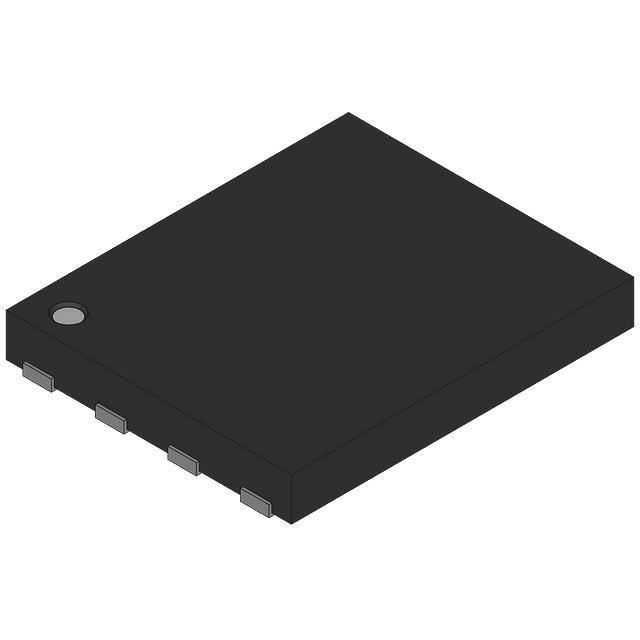


 工商网监
湘ICP备2023018690号
工商网监
湘ICP备2023018690号

