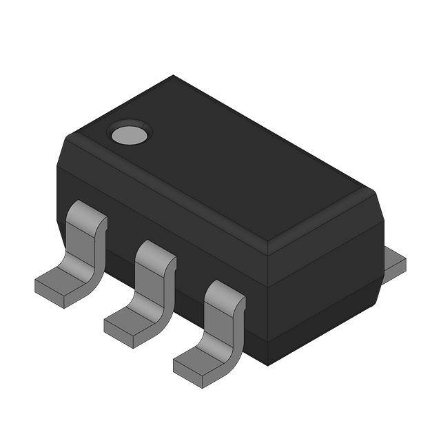
R1225N Series
PWM/VFM Step-down DC/DC Controller
NO.EA-097-181004
OUTLINE
The R1225N is a CMOS-based PWM step-down DC/DC converter controller with low supply current. It consists
of an oscillator, a PWM control circuit, a reference voltage unit, an error amplifier, a soft-start circuit, a latchtype protection circuit, a PWM/VFM alternative circuit, a chip enable circuit, a phase compensation circuit, and
an input voltage detect circuit. Further, protection circuit delay time adjuster circuit, and resistors for voltage
detection are included. A low ripple, high efficiency step-down DC/DC converter can be easily composed of
this IC with some external components, or a power-transistor, an inductor, a diode and capacitors. With a
PWM/VFM alternative circuit, when the load current is small, the operation is automatically switching into the
VFM oscillator from PWM oscillator, therefore the efficiency at small load current is improved. The
R1225NxxxC/D/K types, which are without a PWM/VFM alternative circuit, are also available.
If the term of maximum duty cycle keeps on a certain time, the embedded protection circuit works. It is latchtype protection circuit, and it works to latch an external Power MOSFET with keeping it off. To release the
condition of protection, after disable this IC with a chip enable circuit, enable it again, or restart this IC with
power-on. Delay Time for protection circuit is adjustable with an external capacitor. With a built-in UVLO
function, when the input voltage is UVLO threshold or less, this IC keeps standby state, and saves its
consumption current and avoids miss-operation. Further, if the set output voltage is equal or more than 2.1 V,
with a built-in start-up function, at the power-on moment until the input voltage becomes more than the set
output voltage, DC/DC operation is halted and avoids miss-operation.
FEATURES
•
•
•
•
•
•
•
•
Wide Range of Input Voltage ........................................................... 2.3 V to 18.5 V
Built-in Soft-start and Latch-type Protection
Three Options of Oscillator Frequency ............................................ 180 kHz, 300 kHz, 500 kHz
High Efficiency ................................................................................. Typ. 90%
Output Voltage ................................................................................. 1.2 V to 6.0 V, 0.1 V step
Standby Current............................................................................... Typ. 0.0 µA
High Accuracy Output Voltage ......................................................... ±2.0%
Low Temperature-Drift Coefficient of Output Voltage ...................... Typ. ±100 ppm/°C
APPLICATIONS
• Hand-held Communication Equipment, Cameras, VCRs, Camcorders
• Battery-powered Equipment
• Household Electrical Appliances
1
�R1225N
NO.EA-097-181004
BLOCK DIAGRAM
R1225N Block Diagram
SELECTION GUIDE
The output voltage, the oscillator frequency and the PWM/VFM alternative circuit are user-selectable options.
Selection Guide
Product Name
R1225Nxx2∗-TR-FE
Package
Quantity per Reel
Pb Free
Halogen Free
SOT-23-6W
3,000 pcs
Yes
Yes
xx: The output voltage can be designed in the range from 1.2 V (12) to 6.0 V (60) in 0.1 V steps.
∗: The oscillator frequency and the modulation method are options as follows.
∗
A
B
C
D
J
K
2
Oscillator
Frequency
300 kHz
500 kHz
300 kHz
500 kHz
180 kHz
180 kHz
PWM/VFM Alternative
Circuit
Yes
Yes
No
No
Yes
No
�R1225N
NO.EA-097-181004
PIN DESCRIPTIONS
6
5
4
(mark side)
1
2
3
R1225N (SOT-23-6W) Pin Configuration
Pin Description
Pin No.
Symbol
1
EXT
External Transistor Drive Pin, CMOS Output Type
2
VIN
Power Supply Pin
3
DLY
Pin for Setting External Capacitor for Protection Circuit Delay Time
4
CE
Chip Enable Pin, Active-high
5
GND
Ground Pin
6
VOUT
Pin for Monitoring Output Voltage
Description
3
�R1225N
NO.EA-097-181004
ABSOLUTE MAXIMUM RATINGS
Absolute Maximum Ratings
Symbol
VIN
Item
Rating
VIN Supply Voltage
(GND = 0 V)
Unit
20
V
VEXT
EXT Pin Output Voltage
−0.3 to VIN+0.3
V
VCE
CE Pin Input Voltage
−0.3 to VIN+0.3
V
VOUT
VOUT Pin Input Voltage
−0.3 to VIN+0.3
V
VDLY
VDLY Pin Input Voltage
−0.3 to 1.0
V
IEXT
EXT Pin Inductor Drive Output Current
±50
mA
IDLY
DLY Pin Output Current
±15
mA
PD
Power Dissipation
430
mW
Tj
Junction Temperature Range
−40 to 125
°C
Tstg
Storage Temperature Range
−55 to 125
°C
ABSOLUTE MAXIMUM RATINGS
Electronic and mechanical stress momentarily exceeded absolute maximum ratings may cause the permanent
damages and may degrade the lifetime and safety for both device and system using the device in the field. The
functional operation at or over these absolute maximum ratings is not assured.
RECOMMENDED OPERATING CONDITIONS
Recommended Operating Conditions
Symbol
Item
Rating
Unit
VIN
Input Voltage
2.3 to 18.5
V
Ta
Operating Temperature Range
−40 to 85
°C
RECOMMENDED OPERATING CONDITIONS
All of electronic equipment should be designed that the mounted semiconductor devices operate within the
recommended operating conditions. The semiconductor devices cannot operate normally over the recommended
operating conditions, even if when they are used over such conditions by momentary electronic noise or surge. And the
semiconductor devices may receive serious damage when they continue to operate over the recommended operating
conditions.
4
�R1225N
NO.EA-097-181004
ELECTRICAL CHARACTERISTICS
R1225Nxx2X Electrical Characteristics (X = A/ B/ C/ D/ J/ K)
Symbol
Item
Conditions
VOUT
∆VOUT/
∆Ta
fOSC
ΔfOSC/
ΔTa
Step-down Output
Voltage
Step-down Output
Voltage Temperature
Coefficient
VIN = VCE = VSET + 1.5 V, IOUT = -100 mA
When VSET ≤ 1.5 V, VIN = VCE = 3.0 V
(Ta = 25°C)
Min. Typ. Max. Unit
VSET
VSET
VSET
V
×0.98
×1.02
-40°C ≤ Ta ≤ 85°C
Oscillator Frequency
VIN = VCE = VSET + 1.5 V, IOUT = -100 mA
When VSET ≤ 1.5 V, VIN = VCE = 3.0 V
J/ K version
A/ C version
B/ D version
Oscillator Frequency
Temperature Coefficient
-40°C ≤ Ta ≤ 85°C
144
240
400
IEXTH
EXT “H” Output Current
IEXTL
EXT “L” Output Current
ISW
DLY switch current
ICEH
CE “H” Input Current
VIN = VCE = VOUT = 18.5 V
ICEL
CE “L” Input Current
VIN = VOUT = 18.5 V, VCE = 0 V
-0.5
VCEH
CE “H” Input Voltage
VIN = 8 V, VOUT = 0 V
1.5
VCEL
CE “L” Input Voltage
Oscillator Maximum
Duty Cycle
VFM Duty Cycle
VIN = 8 V, VOUT = 0 V
A/ B/ J version
VUVLO1
UVLO Voltage
VOUT = 0 V, VIN = VCE = 2.5 V→1.5 V
V UVLO2
UVLO Release Voltage
VOUT = 0 V, VIN = VCE = 1.5 V→2.5 V
tSTART
Soft-start Time
tPROT
Protection Delay Time
Supply Current 1
ISTANDBY
Standby Current
DMAX
DVFM
180
300
500
216
360
600
20
30
40
0.0
50
60
80
0.5
µA
-17
-10
mA
µA
20
30
mA
1.0
2.0
mA
0.0
0.5
0.0
V
0.3
V
%
35
1.8
µA
µA
100
VIN = VSET + 1.5 V, IOUT = -10 mA
VCE = 0 V→VSET + 1.5 V
VIN = VCE = VSET + 1.5 V
VOUT = VSET + 1.5 V→0 V
kHz
%/
°C
±0.2
VIN = VCE = VOUT = 18.5 V
A/ B/ J/ K version
C version
D version
VIN = 18.5 V, VCE = 0 V, VOUT = 0 V
VIN = 8 V, VEXT = 7.9 V, VOUT = 8 V, VCE
=8V
VIN = 8 V, VEXT = 0.1 V, VOUT = 0 V, VCE
=8V
VIN = 2.3 V, VCE = 0 V, VDLY = 0.1 V
IDD1
ppm/
°C
±100
%
2.0
VUVLO1
+0.1
2.2
V
2.3
V
5
10
20
ms
10
20
35
ms
5
�R1225N
NO.EA-097-181004
TYPICAL APPLICATION AND APPLICATION HINTS
Typical Application
External Components
Symbol
PMOS
L
6
uPA1914, Renesas
CR105NP-270MC, Sumida
SD
CMS06, Toshiba
C1
10 µF, Ceramic Type
C2
0.1 µF, Ceramic Type
C3
47 µF, Tantalum Type
C4
0.02 µF, Ceramic Type
R1
10 Ω
Description
�R1225N
NO.EA-097-181004
TECHNICAL NOTES
• As shown in the block diagram, a parasitic diode is formed in each terminal, each of these diodes is not
formed for load current, therefore do not use it in such a way. When you control the CE pin by another power
supply, do not make its “H” level more than the voltage level of VIN pin.
• The operation of Latch-type protection circuit is as follows;
When the maximum duty cycle continues longer than the delay time for protection circuit, (Refer to the
Electrical Characteristics) the protection circuit works to shutdown Power MOSFET with latching operation.
Therefore when an input/output voltage difference is small, the protection circuit may work with small load
current.
To release the protection of latch status, after disable this IC with a chip enable circuit, enable it again, or
restart this IC with power-on. However, in the case of restarting this IC with power-on, after the power supply
is turned off, if a certain amount of charge remains in CIN, or some voltage is forced to VIN from CIN, this IC
might not be restarted even after power-on.
• Set external components as close as possible to the IC and minimize the connection between the
components and the IC. In particular, a capacitor should be connected to VOUT pin with the minimum
connection. Make grounding sufficient and reinforce supplying. Large switching current flows through the
connection of power line, an inductor and the connection of VOUT. If the impedance of the connection of
power supply is high, the voltage level of power supply of the IC fluctuates with the switching current. This
may cause unstable operation of the IC.
• Use capacitors with a capacity of 22 µF or more for VOUT pin, and with good high frequency characteristics
such as tantalum capacitors. We recommend to use capacitors with an allowable voltage which is at least
twice as much as setting output voltage, in terms of the input capacitors, its voltage rating is twice or more
than input voltage. This is because there may be a case where a spike-shaped high voltage is generated by
an inductor when an external transistor is on and off.
• Choose an inductor that has sufficiently small D.C. resistance and large allowable current and is hard to
reach magnetic saturation. If the value of inductance of an inductor is extremely small, the ILX may exceed
the absolute maximum rating at the maximum loading. Use an inductor with appropriate inductance.
• Use a diode of a Schottky type with high switching speed, and also pay attention to its current capacity.
• Do not use this IC under the condition with VIN voltage at equal or less than minimum operating voltage.
• When the threshold level of an external power MOSFET is rather low and the drive-ability of voltage supplier
is small, if the output pin is short circuit, input voltage may be equal or less than UVLO detector threshold.
In this case, the devise is reset with UVLO function that is not the latch-protection function.
• With the PWM/VFM alternative circuit, when the on duty cycle of switching is 35% or less, the R1225N alters
from PWM mode to VFM mode (Pulse skip mode). The purpose of this circuit is raising the efficiency with a
light load by skipping the frequency and suppressing the consumption current. However, the ratio of output
voltage against input voltage is 35% or less, (ex. VIN > 8.6 V and VOUT = 3.0 V) even if the large current may
be loaded, the IC keeps its VFM mode. As a result, frequency might be decreased, and oscillation waveform
might be unstable. These phenomena are the typical characteristics of the IC with PWM/VFM alternative
circuit.
The performance of a power source circuit using this device is highly dependent on a peripheral circuit. A
peripheral component or the device mounted on PCB should not exceed its rated voltage, rated current or
rated power. When designing a peripheral circuit, please be fully aware of the following points.
7
�R1225N
NO.EA-097-181004
HOW TO SET THE DELAY TIME FOR PROTECTION CIRCUIT
The equation describes how to calculate the delay time of protection circuit from the value of an external
capacitor C4.
tDLY = C4 x 106sec (in this equation, 1 µF ≥ C4 ≥ 1000 pF)
Without the external capacitor, a certain delay time exists, therefore, if the external capacitor is less than 1000
pF, the error will increase. Further, if the external capacitor value is beyond 1 µF, the time required to discharge
the C4 will be long, and this may cause the miss-operation. For example, if the protection circuit may work and
released, soon after that the protection may work. In that case, C4 has not discharged completely yet, therefore,
the delay time may be shorter than expected.
8
�R1225N
NO.EA-097-181004
OPERATION OF STEO-DOWN DC/DC CONVERTER AND OUTPUT
CURRENT
The step-down DC/DC converter charges energy in the inductor when Lx transistor is ON, and discharges the
energy from the inductor when Lx transistor is OFF and controls with less energy loss, so that a lower output
voltage than the input voltage is obtained. The operation will be explained with reference to the following
diagrams:
Basic Circuits
Current through L
Step 1: Lx Tr. turns on and current IL (= i1) flows, and energy is charged into CL. At this moment, IL increases
from ILmin (= 0) to reach ILmax in proportion to the on-time period (ton) of LX Tr.
Step 2: When Lx Tr. turns off, Schottky diode (SD) turns on in order that L maintains IL at ILmax, and current
IL (= i2) flows.
Step 3: IL decreases gradually and reaches ILmin after a time period of topen, and SD turns off, provided that
in the continuous mode, next cycle starts before IL becomes to 0 because toff time is not enough. In
this case, IL value is from this ILmin (> 0).
In the case of PWM control system, the output voltage is maintained by controlling the on-time period (ton),
with the oscillator frequency (fOSC) being maintained constant.
9
�R1225N
NO.EA-097-181004
Discontinuous Conduction Mode and Continuous Conduction Mode
The maximum value (ILmax) and the minimum value (ILmin) current which flow through the inductor is the
same as those when Lx Tr. turns on and when it turns off.
The difference between ILmax and ILmin, which is represented by ∆I;
∆I = Ilmax – Ilmin = VOUT x topen / L= (VIN – VOUT) x ton / L .............Equation 1
Where, T = 1 / fOSC = ton + toff
Duty (%) = ton / T x 100 = ton x fOSC x 100
topen ≤ toff
In Equation 1, VOUT x topen / L and (VIN - VOUT) x ton / L are respectively shown the change of the current at
ON, and the change of the current at OFF.
When the output current (IOUT) is relatively small, topen < toff as illustrated in the above diagram. In this case,
the energy is charged in the inductor during the time period of ton and is discharged in its entirely during the
time period of toff, therefore ILmin becomes to zero (ILmin = 0). When IOUT is gradually increased, eventually,
topen becomes to toff (topen = toff), and when IOUT is further increased, ILmin becomes larger than zero (ILmin
> 0). The former mode is referred to as the discontinuous mode and the latter mode is referred to as continuous
mode.
In the continuous mode, when Equation 1 is solved for ton and assumed that the solution is tonc,
tonc = T x VOUT / VIN ..........................................................................Equation 2
When ton < tonc, the mode is the discontinuous mode, and when ton = tonc, the mode is the continuous mode.
10
�R1225N
NO.EA-097-181004
OUTPUT CURRENT AND SELECTION OF EXTERNAL COMPONENTS
When Lx Tr. is “ON”:
(Wherein, Ripple Current P-P value is described as IRP, ON resistance of LX Tr. is described as RP the direct
current of the inductor is described as RL.)
VIN = VOUT + (RP + RL) x IOUT + L x IRP / ton .......................................Equation 3
When Lx Tr. is “OFF”:
L x IRP / toff = VF + VOUT + RL x IOUT ...................................................Equation 4
Put Equation 4 to Equation 3 and solve for ON duty, ton / (toff + ton) = DON,
DON = (VOUT + VF + RL x IOUT) / (VIN + VF – RP x IOUT) ........................Equation 5
Ripple Current is as follows;
IRP = (VIN – VOUT – RP x IOUT – RL x IOUT) x DON / f / L ........................Equation 6
Wherein, peak current that flows through L, Lx Tr., and SD is as follows;
ILmax = IOUT + IRP / 2 .........................................................................Equation 7
Consider ILmax, condition of input and output and select external components.
The above explanation is directed to the calculation in an ideal case in continuous mode.
11
�R1225N
NO.EA-097-181004
EXTERNAL COMPONENTS
1.
Inductor
Select an inductor that peak current does not exceed ILmax. If larger current than allowable current flows,
magnetic saturation occurs and make transform efficiency worse. When the load current is definite, the
smaller value of L, the larger the ripple current. Provided that the allowable current is large in that case
and DC current is small, therefore, for large output current, efficiency is better than using an inductor with
a large value of L and vice versa.
2.
Diode
Use a diode with low VF (Schottky type is recommended.) and high switching speed. Reverse voltage
rating should be more than VIN and current rating should be equal or more than ILmax.
3.
Capacitors
As for CIN, use a capacitor with low ESR (Equivalent Series Resistance) and a capacity of at least 10 µF
for stable operation. COUT can reduce ripple of Output Voltage, therefore 47 µF or more value of tantalum
type capacitor is recommended.
4. Lx Transistor
Pch Power MOSFET is required for this IC. Its breakdown voltage between gate and source should be a
few V higher than Input Voltage. In the case of Input Voltage is low, to turn on MOSFET completely, to use
a MOSFET with low threshold voltage is effective. If a large load current is necessary for your application
and important, choose a MOSFET with low ON resistance for good efficiency. If a small load current is
mainly necessary for your application, choose a MOSFET with low gate capacity for good efficiency.
Maximum continuous drain current of MOSFET should be larger than peak current, ILmax.
12
�R1225N
NO.EA-097-181004
TIMING CHART
Case 1. Set VOUT Voltage > 2.1 V (Set VOUT Voltage > UVLO Voltage)
The timing chart shown above describes the changing process of input voltage rising, stable operating,
operating with large current, reset with CE pin, stable operating, input voltage falling, input voltage recovering,
and stable operating.
First, until when the input voltage (VIN) reaches the set output voltage, the circuit inside keeps the condition of
pre-standby.
Second, after VIN becomes beyond the set output voltage, soft-start operation starts, when the soft-start
operation finishes, the operation becomes stable.
If too large current flows through the circuit because of short or other reasons, EXT signal ignores that during
the delay time of protection circuit. (The current value depends on the circuit.)
After the delay time passes, the latch protection works, or EXT signal will be “H”, then output will turn off. To
release the latch protection, input voltage should be equal or lower than UVLO level, or restart with CE (Once
turn off the circuit with CE and turn it on again). In the timing charge above, release the latch function is realized
with CE signal from “L” to “H”. After removing the cause of large current and the reset with CE, soft-start
operation starts and after the soft-start time, the operation will be back to stable.
If the VIN becomes lower than the set VOUT, that situation is same as large current condition, so protection
circuit may be ready to work, therefore, after the delay time of protection circuit, EXT will be “H” and the output
turns off.
Further, if the VIN is lower than UVLO voltage, the circuit inside will be stopped by UVLO function.
After that, if VIN rises, until when the VIN reaches the set output voltage, the circuit inside keeps the condition
of pre-standby. Then after VIN becomes beyond the set output voltage, soft-start operation starts, when the
soft-start operation finishes, the operation becomes stable.
13
�R1225N
NO.EA-097-181004
Case 2. Set VOUT Voltage ≤ 2.0 V (Set VOUT Voltage < UVLO Voltage)
The timing chart shown above describes the changing process of input voltage rising, stable operating,
operating with large current, reset with CE pin, stable operating, input voltage falling, input voltage recovering,
and stable operating.
First, until when the input voltage (VIN) reaches the UVLO voltage, the circuit inside keeps the condition of prestandby. Second, after VIN becomes beyond the UVLO voltage, soft-start operation starts, when the soft-start
operation finishes, the operation becomes stable. If too large current flows through the circuit because of short
or other reasons, EXT signal ignores that during the delay time of protection circuit. (The current value depends
on the circuit.) After the delay time passes, the latch protection works, or EXT signal will be “H”, then output
will turn off. To release the latch protection, input voltage should be equal or lower than UVLO level, or restart
with CE (Once turn off the circuit with CE and turn it on again). In the timing charge above, release the latch
function is realized with CE signal from “L” to “H”. After removing the cause of large current and the reset with
CE, soft-start operation starts and after the soft-start time, the operation will be back to stable. Further, if the
VIN is lower than UVLO voltage, the circuit inside will be stopped by UVLO function. After that, if VIN rises, until
when the VIN reaches UVLO voltage, the circuit inside keeps the condition of pre-standby. Then after VIN
becomes beyond the UVLO voltage, soft-start operation starts, when the soft-start operation finishes, the
operation becomes stable.
14
�R1225N
NO.EA-097-181004
TEST CIRCUITS
A) Output Voltage, Oscillator Frequency, CE “H” Input Voltage, CE “L” Input Voltage, Soft-start time
B) Supply Current 1
C) Standby Current
D) EXT “H” Output Current
E) EXT “L” Output Current
F) DLY Switching Current
15
�R1225N
NO.EA-097-181004
G) CE “H” Input Current, CE “L” Input
Current
H) Output Delay Time for Protection Circuit
External Components
Symbol
PMOS
16
Description
Pch Power MOS, Hitachi: HAT1020R
L1
27 µH, Sumida: CD104NP-270MC
D1
Schottky Type, ROHM: RB491D
C1
47 µF, Tantalum Type
C2
47 µF, Tantalum Type
C3
0.02 µF, Ceramic Type
�R1225N
NO.EA-097-181004
TYPICAL CHARACTERISTICS
1) Efficiency vs. Output Current
R1225N182A (VIN=3.3V)
CDRH127-10µH
R1225N182A (VIN=5.0V)
CDRH127-10µH
R1225N182B (VIN=3.3V)
CDRH127-10µH
R1225N182B (VIN=5.0V)
CDRH127-10µH
17
�R1225N
NO.EA-097-181004
18
R1225N182C (VIN=3.3V)
CDRH127-10µH
R1225N182C (VIN=5.0V)
CDRH127-10µH
R1225N182C (VIN=12V)
CDRH127-10µH
R1225N182D (VIN=3.3V)
CDRH127-10µH
R1225N182D (VIN=5.0V)
CDRH127-10µH
R1225N182D (VIN=12V)
CDRH127-10µH
�R1225N
NO.EA-097-181004
R1225N182J (VIN=3.3V)
CDRH127-27µH
R1225N182J (VIN=5.0V)
CDRH127-27µH
R1225N182K (VIN=3.3V)
CDRH127-27µH
R1225N182K (VIN=5.0V)
CDRH127-27µH
R1225N182K (VIN=12V)
CDRH127-27µH
R1225N332A (VIN=4.8V)
CDRH127-10µH
19
�R1225N
NO.EA-097-181004
20
R1225N332A (VIN=7.0V)
CDRH127-10µH
R1225N332B (VIN=4.8V)
CDRH127-10µH
R1225N332B (VIN=7.0V)
CDRH127-10µH
R1225N332C (VIN=4.8V)
CDRH127-10µH
R1225N332C (VIN=12V)
CDRH127-10µH
R1225N332C (VIN=15V)
CDRH127-10µH
�R1225N
NO.EA-097-181004
R1225N332D (VIN=4.8V)
CDRH127-10µH
R1225N332D (VIN=12V)
CDRH127-10µH
R1225N332D (VIN=15V)
CDRH127-10µH
R1225N332K (VIN=4.8V)
CDRH127-27µH
R1225N332K (VIN=12V)
CDRH127-27µH
R1225N332K (VIN=15V)
CDRH127-27µH
21
�R1225N
NO.EA-097-181004
22
R1225N502A (VIN=6.5V)
CDRH127-10µH
R1225N502A (VIN=10V)
CDRH127-10µH
R1225N502B (VIN=6.5V)
CDRH127-10µH
R1225N502B (VIN=10V)
CDRH127-10µH
R1225N502C (VIN=6.5V)
CDRH127-10µH
R1225N502C (VIN=12V)
CDRH127-10µH
�R1225N
NO.EA-097-181004
R1225N502C (VIN=15V)
CDRH127-10µH
R1225N502D (VIN=6.5V)
CDRH127-10µH
R1225N502D (VIN=12V)
CDRH127-10µH
R1225N502D (VIN=15V)
CDRH127-10µH
R1225N502J (VIN=6.5V)
CDRH127-27µH
R1225N502J (VIN=10V)
CDRH127-27µH
23
�R1225N
NO.EA-097-181004
R1225N502K (VIN=6.5V)
CDRH127-27µH
R1225N502K (VIN=15V)
CDRH127-27µH
R1225N502K (VIN=12V)
CDRH127-27µH
2) Ripple Voltage vs. Output Current
R1225N182A
24
L=10µH
R1225N182B
L=10µH
�R1225N
NO.EA-097-181004
R1225N182C
L=10µH
R1225N182D
L=10µH
R1225N182J
L=27µH
R1225N182K
L=27µH
R1225N332A
L=10µH
R1225N332B
L=10µH
25
�R1225N
NO.EA-097-181004
26
R1225N332C
L=10µH
R1225N332D
L=10µH
R1225N332J
L=27µH
R1225N332K
L=27µH
R1225N502A
L=10µH
R1225N502B
L=10µH
�R1225N
NO.EA-097-181004
R1225N502C
L=10µH
R1225N502D
L=10µH
R1225N502J
L=27µH
R1225N502K
L=27µH
R1225N182B
L=10µH
3) Input Voltage vs. Output Voltage
R1225N182A
L=10µH
27
�R1225N
NO.EA-097-181004
28
R1225N182C
L=10µH
R1225N182D
L=10µH
R1225N182J
L=27µH
R1225N182K
L=27µH
R1225N332A
L=10µH
R1225N332B
L=10µH
�R1225N
NO.EA-097-181004
R1225N332C
L=10µH
R1225N332D
L=10µH
R1225N332J
L=27µH
R1225N332K
L=27µH
R1225N182B
L=10µH
4) Output Voltage vs. Output Current
R1225N182A
L=10µH
29
�R1225N
NO.EA-097-181004
30
R1225N182C
L=10µH
R1225N182D
L=10µH
R1225N182J
L=27µH
R1225N182K
L=27µH
R1225N332A
L=10µH
R1225N332B
L=10µH
�R1225N
NO.EA-097-181004
R1225N332C
L=10µH
R1225N332D
L=10µH
R1225N332J
L=27µH
R1225N332K
L=27µH
R1225N502A
L=10µH
R1225N502B
L=10µH
31
�R1225N
NO.EA-097-181004
R1225N502C
L=10µH
R1225N502D
L=10µH
R1225N502J
L=27µH
R1225N502K
L=27µH
5) Load Transient Response
R1225N332A
32
L=10µH
VIN=4.8V
R1225N332A
L=10µH
VIN=4.8V
�R1225N
NO.EA-097-181004
R1225N332A
R1225N332B
R1225N332B
L=10µH
L=10µH
L=10µH
VIN=7V
VIN=4.8V
VIN=7V
R1225N332A
R1225N332B
R1225N332B
L=10µH
L=10µH
L=10µH
VIN=7V
VIN=4.8V
VIN=7V
33
�R1225N
NO.EA-097-181004
R1225N332J
R1225N332J
34
L=27µH
L=10µH
VIN=4.8V
VIN=7V
R1225N332J
R1225N332J
L=27µH
L=27µH
VIN=4.8V
VIN=7V
�1. The products and the product specifications described in this document are subject to change or discontinuation of
production without notice for reasons such as improvement. Therefore, before deciding to use the products, please
refer to Ricoh sales representatives for the latest information thereon.
2. The materials in this document may not be copied or otherwise reproduced in whole or in part without prior written
consent of Ricoh.
3. Please be sure to take any necessary formalities under relevant laws or regulations before exporting or otherwise
taking out of your country the products or the technical information described herein.
4. The technical information described in this document shows typical characteristics of and example application circuits
for the products. The release of such information is not to be construed as a warranty of or a grant of license under
Ricoh's or any third party's intellectual property rights or any other rights.
5. The products listed in this document are intended and designed for use as general electronic components in standard
applications (office equipment, telecommunication equipment, measuring instruments, consumer electronic products,
amusement equipment etc.). Those customers intending to use a product in an application requiring extreme quality
and reliability, for example, in a highly specific application where the failure or misoperation of the product could result
in human injury or death (aircraft, spacevehicle, nuclear reactor control system, traffic control system, automotive and
transportation equipment, combustion equipment, safety devices, life support system etc.) should first contact us.
6. We are making our continuous effort to improve the quality and reliability of our products, but semiconductor products
are likely to fail with certain probability. In order to prevent any injury to persons or damages to property resulting from
such failure, customers should be careful enough to incorporate safety measures in their design, such as redundancy
feature, fire containment feature and fail-safe feature. We do not assume any liability or responsibility for any loss or
damage arising from misuse or inappropriate use of the products.
7. Anti-radiation design is not implemented in the products described in this document.
8. The X-ray exposure can influence functions and characteristics of the products. Confirm the product functions and
characteristics in the evaluation stage.
9. WLCSP products should be used in light shielded environments. The light exposure can influence functions and
characteristics of the products under operation or storage.
10. There can be variation in the marking when different AOI (Automated Optical Inspection) equipment is used. In the
case of recognizing the marking characteristic with AOI, please contact Ricoh sales or our distributor before attempting
to use AOI.
11. Please contact Ricoh sales representatives should you have any questions or comments concerning the products or
the technical information.
Halogen Free
Ricoh is committed to reducing the environmental loading materials in electrical devices
with a view to contributing to the protection of human health and the environment.
Ricoh has been providing RoHS compliant products since April 1, 2006 and Halogen-free products since
April 1, 2012.
https://www.e-devices.ricoh.co.jp/en/
Sales & Support Offices
Ricoh Electronic Devices Co., Ltd.
Shin-Yokohama Office (International Sales)
2-3, Shin-Yokohama 3-chome, Kohoku-ku, Yokohama-shi, Kanagawa, 222-8530, Japan
Phone: +81-50-3814-7687 Fax: +81-45-474-0074
Ricoh Americas Holdings, Inc.
675 Campbell Technology Parkway, Suite 200 Campbell, CA 95008, U.S.A.
Phone: +1-408-610-3105
Ricoh Europe (Netherlands) B.V.
Semiconductor Support Centre
Prof. W.H. Keesomlaan 1, 1183 DJ Amstelveen, The Netherlands
Phone: +31-20-5474-309
Ricoh International B.V. - German Branch
Semiconductor Sales and Support Centre
Oberrather Strasse 6, 40472 Düsseldorf, Germany
Phone: +49-211-6546-0
Ricoh Electronic Devices Korea Co., Ltd.
3F, Haesung Bldg, 504, Teheran-ro, Gangnam-gu, Seoul, 135-725, Korea
Phone: +82-2-2135-5700 Fax: +82-2-2051-5713
Ricoh Electronic Devices Shanghai Co., Ltd.
Room 403, No.2 Building, No.690 Bibo Road, Pu Dong New District, Shanghai 201203,
People's Republic of China
Phone: +86-21-5027-3200 Fax: +86-21-5027-3299
Ricoh Electronic Devices Shanghai Co., Ltd.
Shenzhen Branch
1205, Block D(Jinlong Building), Kingkey 100, Hongbao Road, Luohu District,
Shenzhen, China
Phone: +86-755-8348-7600 Ext 225
Ricoh Electronic Devices Co., Ltd.
Taipei office
Room 109, 10F-1, No.51, Hengyang Rd., Taipei City, Taiwan
Phone: +886-2-2313-1621/1622 Fax: +886-2-2313-1623
�