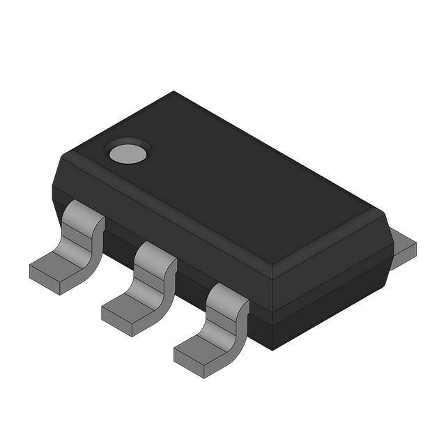
R1245x Series
1.2 A, 30 V Step-Down DC/DC Converter
No. EA-269-170720
OUTLINE
The R1245x is a CMOS-based Step-down DC/DC converter with internal N-channel high side Tr. The ON
resistance of the built-in high-side transistor is 0.35 Ω and the R1245x can provide the maximum 1.2 A output
current. Each of the ICs consists of an oscillator, a PWM control circuit, a voltage reference unit, an error
amplifier, a phase compensation circuit, a slope compensation circuit, a soft-start circuit, protection circuits, an
internal voltage regulator, and a switch for bootstrap circuit. The ICs can make up a step-down DC/DC
converter with an inductor, resistors, a diode, and capacitors.
The R1245x is a current mode operating type DC/DC converter without an external current sense resistor, and
realizes fast response and high efficiency. As an output capacitor, a ceramic type capacitor can be used with
the R1245x. The options of the internal oscillator frequency are preset at 330 kHz for version A and B, 500
kHz for version C and D, 1000 kHz for version E and F, 2400 kHz for version G and H.
As for protection, an Lx peak current limit circuit cycle by cycle, a thermal shutdown function and an under
voltage lockout (UVLO) function are built in. Furthermore, there are two types for short protection, for A/C/E/G
version, a latch protection function which makes the output latch off if the output voltage keeps lower than the
set output voltage for a certain time after detecting current limit is built in, for B/D/F/H version, a fold-back
protection function which changes the oscillator frequency slower after detecting short circuit or equivalent.
As for the packages of the R1245x, HSOP-8E, DFN(PLP)2020-8, SOT23-6W are available.
FEATURES
•
•
•
•
•
•
•
•
•
•
•
•
Operating Voltage
·········································· 4.5 V to 30 V
Internal N-channel MOSFET Driver ······················ Typ. RON = 0.35 Ω
Adjustable Output Voltage with External Resistor ···· 0.8 V or more
Feedback Voltage and Tolerance ························· 0.8 V±1.0%
Peak Current Limit ············································ Typ. 2.0 A
UVLO Function Released Voltage ························ Typ. 4.0 V
Operating Frequency ········································ 330 kHz (Ver. A/B), 500 kHz (Ver. C/D),
1000 kHz (Ver. E/F), 2400 kHz (Ver. G/H)
Fold-back Protected Frequency ··························· 170 kHz (Ver. B/D), 250 kHz (Ver. F), 400 kHz (Ver. H)
Latch Protection Delay Time ······························· Typ. 4 ms (Ver. A/C/E/G)
Ceramic Capacitors Recommended for Input and Output.
Stand-by Current ·············································· Typ. 0 µA
Packages ······················································· SOT-23-6W, DFN(PLP)2020-8, HSOP-8E
1
�R1245x
No. EA-269-170720
APPLICATIONS
•
•
•
•
Digital Home Appliances: Digital TVs, DVD Players
Office Equipment: Printers, Faxes
5V PSU or 2-cell or more Li-ion Battery Powered Communication Equipment, Cameras, VCRs, Camcorders
High Voltage Battery-powered Equipment
SELECTION GUIDE
In the R1245x, the package, type of short protection (Latch or Fold-back), and the oscillator frequency can be
selected with the user’s request.
Selection Guide
Product code
Package
Quantity per Reel
Pb Free
Halogen Free
R1245S003∗-E2-FE
HSOP-8E
1,000 pcs
Yes
Yes
DFN(PLP)2020-8
5,000 pcs
Yes
Yes
SOT-23-6W
3,000 pcs
Yes
Yes
R1245K003∗-TR
R1245N001∗-TR-FE
∗: Designation of the oscillator frequency and the protection function option.
Oscillator
Latch
Fold-back
Symbol
Frequency
Protection
Protection
A
330 kHz
B
330 kHz
C
500 kHz
D
500 kHz
E
1000 kHz
F
1000 kHz
G
2400 kHz
H
2400 kHz
2
�R1245x
No. EA-269-170720
BLOCK DIAGRAM
VIN
Thermal Shutdown
UVLO
CE
Regulator
Regulator
5V
BST
Shutdown
SETPULSE
Oscillator
*1
FB
MAXDUTY
S
D
Lx
R
Reference
+
+
Soft Start
Circuit(1ms)
0.8V
Limit Latch
Circuit (4ms)
*1
Current Slope
Circui
t
Peak Current
Limit Circuit
GND
R1245x Block Diagram
*1
Version
A
B
C
D
E
F
G
H
Oscillator Frequency
330 kHz
330 kHz
500 kHz
500 kHz
1000 kHz
1000 kHz
2400 kHz
2400 kHz
Short Protection Type
330 kHz
330 kHz
500 kHz
500 kHz
1000 kHz
1000 kHz
2400 kHz
2400 kHz
3
�R1245x
No. EA-269-170720
PIN DESCRIPTIONS
Top View
Bottom View
8
7
6
5
5
6
7
8
1
2
3
4
4
3
2
1
DFN(PLP)2020-8 Pin Configuration
Top View
8
1
7
2
6
3
Top View
Bottom View
5
4
5
4
6
3
7
2
HSOP-8E Pin Configuration
8
6
5
4
1
2
3
1
SOT-23-6W Pin Configuration
* Connect the backside heat radiation tub to GND or same as GND level (recommendation). The tub is
connected to the GND pin.
4
�R1245x
No. EA-269-170720
R1245S Pin Description
Pin No.
Symbol
Description
1
Lx
Lx Switching Pin
2
VIN
Power Supply Pin
3
CE
Chip Enable Pin, Active with ”H”
4
TEST
TEST pin (must be open for user side.)
5
GND
Ground Pin
6
FB
Feedback Pin
7
NC
No connection
8
BST
Bootstrap Pin
* Connect the backside heat radiation tub to GND or same as GND level (recommendation). The tub is connected to the
GND pin.
R1245K Pin Description
Pin No.
Symbol
Description
1
Lx
Lx Switching Pin
2
VIN
Power Supply Pin
3
VIN
Power Supply Pin
4
CE
Chip Enable Pin, Active with ”H”
5
GND
6
FB
7
TEST
8
BST
Ground Pin
Feedback Pin
Test Pin (must be open for user side.)
Bootstrap Pin
* Connect the backside heat radiation tub to GND or same as GND level (recommendation). The tub is connected to the
GND pin.
R1245N Pin Description
Pin No.
Symbol
Description
1
BST
Bootstrap Pin
2
GND
Ground Pin
3
FB
Feedback Pin
4
CE
Chip Enable Pin, Active with ”H”
5
VIN
Power Supply Pin
6
Lx
Lx Switching Pin
5
�R1245x
No. EA-269-170720
INTERNAL EQUIVALENT CIRCUIT FOR EACH PIN
Regulator
VIN
BST
LX
LX
Regulator
Regulator
6
VIN
CE
FB
TEST
�R1245x
No. EA-269-170720
ABSOLUTE MAXMUM RATINGS
(GND = 0 V)
Absolute Maximum Ratings
Symbol
VIN
Item
Rating
Unit
−0.3 V to 32 V
V
VLX −0.3 V to VLX + 6 V
V
Input Voltage
VBST
BST Pin Voltage
VLX
Lx Pin Voltage
−0.3 V to VIN + 0.3
V
VCE
CE Pin Input Voltage
−0.3 V to VIN + 0.3
V
VFB
Feedback Pin Voltage
−0.3 V to 6 V
V
PD
Power
Dissipation*
HSOP-8E
Ultra High Wattage
Land Pattern
2900
DFN(PLP)2020-8
Standard Land Pattern
880
SOT-23-6W
Standard Land Pattern
430
mW
Tj
Junction Temperature Range
−40 to 125
ºC
Tstg
Storage Temperature Range
−55 to 125
ºC
* Refer to POWER DISSIPATION for detailed information.
ABSOLUTE MAXIMUM RATINGS
Electronic and mechanical stress momentarily exceeded absolute maximum ratings may cause the permanent
damages and may degrade the lifetime and safety for both device and system using the device in the field.
The functional operation at or over these absolute maximum ratings is not assured.
RECOMMENDED OPERATING CONDITIONS
Recommended Operating Conditions
Symbol
Item
Rating
VIN
Operating Input Voltage
Ta
Operating Temperature Range
Unit
4.5 to 30
V
−40 to 105
°C
RECOMMENDED OPERATING CONDITIONS
All of electronic equipment should be designed that the mounted semiconductor devices operate within the
recommended operating conditions. The semiconductor devices cannot operate normally over the recommended
operating conditions, even if when they are used over such conditions by momentary electronic noise or surge. And
the semiconductor devices may receive serious damage when they continue to operate over the recommended
operating conditions.
7
�R1245x
No. EA-269-170720
ELECTRICAL CHARACTERISTICS
(Unless otherwise noted, VIN = 12 V, Ta = 25ºC)
Electrical Characteristics
Symbol
Item
Conditions
Min.
Max.
1.0
VUVLO2
−0.1
4.2
0.808
IIN
Consumption Current
VIN = 30 V, VFB = 1.0 V
VUVLO1
UVLO Detect Voltage
Specified VIN falling edge
3.6
VUVLO2
UVLO Released Voltage
Specified rising edge
3.8
−0.2
4.0
0.792
0.800
VFB
ΔVFB/ΔTa
fosc
fFLB
VFB Voltage Tolerance
VFB Voltage Temperature
Coefficient
Oscillator Frequency
Fold back Frequency
±100
−40ºC ≤ Ta ≤ 105ºC
Ver. A/B
300
Ver. C/D
450
500
550
Ver. E/F
900
1000
1100
Ver. G/H
2200
2400
2600
VF B < 0.56 V
Maxduty
tstart
tDLY
RLXH
ILXHOFF
ILIMLXH
VCEL
VCEH
Oscillator Maximum
Duty Cycle
Soft-start Time
Delay Time for Latch
Protection
Lx High Side Switch ON
Resistance
Lx High Side Switch
Leakage Current
Lx High Side Switch Limited
Current
CE “L” Input Voltage
330
Ver. B/D
170
Ver. F
250
Unit
mA
V
V
V
ppm/
ºC
360
kHz
kHz
400
Ver. H
Ver. A/B/C/D
92
Ver. E/F
88
Ver. G/H
76
%
VFB = 0.72 V
1
ms
Ver. A/C/E/G
4
ms
0.35
Ω
VBST − VLX = 4.5 V
VIN = 30 V, VCE = 0 V
VBST − VLX = 4.5 V
1.5
0
5
μA
2.0
2.7
A
0.3
V
VIN = 30 V
1.6
V
CE “H” Input Voltage
VIN = 30 V
IFB
VFB Input Current
VIN = 30.0 V, VFB = 1.0 V
−1.0
1.0
μA
ICEL
CE “L” Input Current
VIN = 30 V, VCE = 0 V
−1.0
1.0
μA
ICEH
CE “H” Input Current
VIN = 30 V, VCE = 30 V
−1.0
1.0
μA
TTSD
Istandby
8
Typ.
0.5
VUVLO2
Thermal Shutdown Detect
Temperature
Standby Current
Hysteresis 30ºC
VIN = 30 V
160
0
ºC
5
μA
�R1245x
No. EA-269-170720
OPERATING DESCRIPTIONS
OPERATION OF THE BUCK CONVERTER AND THE OUTPUT CURRENT
The DC/DC converter charges energy in the inductor when the switch turns on, and discharges the energy
from the inductor when the switch turns off and controls with less energy loss, so that a lower output voltage
than the input voltage is obtained. Refer to the following figures.
ILmax
IL
ILmin
i1
VIN
Switch
L
Diode
i2
topen
VOUT
COUT
GND
ton
toff
t=1/fosc
Basic Circuit
Current flowing through the Inductor
Step 1: The switch turns on and current IL (= i1) flows, and energy is charged into COUT. At this moment, IL
increases from ILmin (= 0) to reach ILmax in proportion to the on-time period (ton) of the switch.
Step 2: When the switch turns off, the diode turns on in order to maintain IL at ILmax, and current IL (= i2)
flows.
Step 3: IL (= i2) decreases gradually and reaches IL = ILmin = 0 after a time period of topen, and the diode
turns off. This case is called as discontinuous mode. If the output current becomes large, next switching cycle
starts before IL becomes 0 and the diode turns off. In this case, IL value increases from ILmin (> 0), and this
case is called continuous mode.
In the case of PWM control system, the output voltage is maintained by controlling the on-time period (ton),
with the oscillator frequency (fosc) being maintained constant.
9
�R1245x
No. EA-269-170720
APPLICATION INFORMATION
TYPICAL APPLICATION CIRCUIT
R1245x00xA/B Typical Application Circuit, 330 kHz, VOUT = 1.2 V, VIN = 24 V
R1245x00xC/D Typical Application Circuit, 500 kHz, VOUT = 3.3 V, VIN = 24 V
* TEST pin must be open.
10
�R1245x
No. EA-269-170720
R1245x00xE/F Typical Application Circuit, 1000 kHz, VOUT = 3.3 V VIN = 12 V
R1245x00xG/H Typical Application Circuit, 2400 kHz, VOUT = 5. 0 V, VIN = 12 V
* TEST pin must be open.
11
�R1245x
No. EA-269-170720
OUTPUT CURRENT AND SELECTION OF EXTERNAL COMPONENTS
The relation between the output current and external components is as follows:
When the switch of Lx turns on:
(Wherein, the peak to peak value of the ripple current is described as IRP, the ON resistance of the switch is
described as RONH, and the diode forward voltage as VF, and the DC resistance of the inductor is described as
RL, and on time of the switch is described as ton)
VIN = VOUT + (RONH + RL) × IOUT + L × IRP / ton ································································· Equation 1
When the switch turns off (the diode turns on) as toff:
L × IRP / toff = VF + VOUT + RL × IOUT ·············································································· Equation 2
Put Equation 2 to Equation 1 and solve for ON duty of the switch, ton / (toff + ton) = DON,
DON = (VOUT + VF + RL × IOUT) / (VIN + VF - RONH × IOUT)······················································ Equation 3
Ripple Current is as follows:
IRP = (VIN − VOUT − RONH × IOUT − RL × IOUT) × DON / fosc / L ················································ Equation 4
wherein, peak current that flows through L, and the peak current ILmax is as follows:
ILmax = IOUT + IRP / 2 ································································································ Equation 5
As for the valley current ILmin,
ILmin = IOUT - IRP / 2 ·································································································· Equation 6
If ILmin < 0, the step-down DC/DC converter operation becomes current discontinuous mode.
Therefore the current condition of the current discontinuous mode, the next formula is true.
IOUT < IRP / 2 ············································································································ Equation 7
Consider ILmax and ILmin, conditions of input and output and select external components.
*The above explanation is based on the calculation in an ideal case in continuous mode.
12
�R1245x
No. EA-269-170720
Ripple Current and Lx Current Limit
The ripple current of the inductor may change according to the various reasons. In the R1245x, as an Lx
current limit, Lx peak current limit is used. Therefore the upper limit of the inductor current is fixed.
The peak current limit is not the average current of the inductor (output current). If the ripple current is large,
peak current becomes also large. The characteristic is used for the fold-back current limit of version B/D/F/H.
In other words, the peak current limit is maintained and the switching frequency is reduced, as a result, the
average current of the inductor is reduced. To release this condition, at 170 kHz for version B/D, at 250 kHz
for version F, at 400 kHz for version H must not be beyond the peak current limit. In the fig.1, the sequence
of the Lx current limit function is described.
VOUT
VOUT
Limit Latch
(R1245x00x
A/C/E/G)
open
4msec
short
4msec
t
shutdown
IOUT
shutdown
restart
(CE=0→"H")
VOUT
VOUT
Fold Back
FB