R1286K SERIES
2ch. PWM Step-up / Inverting DC/DC Converter with Synchronous Rectifier
for AMOLED / LCD
NO.EA-283-191114
OUTLINE
The R1286K 2ch DC/DC converter is designed for AMOLED display power source. It contains a step up DC/DC
converter and an inverting DC/DC converter.
Step up DC/DC converter generates boosted output voltage to 4.6 V to 5.8 V (Selectable). Inverting DC/DC
converter generates negative voltage down to -2.0 V to -6.0 V (Selectable) that is dynamically adjustable with
single wire interface signal. R1286K consist of a voltage reference, error amplifiers, an oscillator, PWM control
circuits, over current protection circuits, short protection circuits, an under voltage lockout circuit (UVLO),
thermal shutdown circuit, a NMOS driver and a synchronous PMOS switch for boost converter, a PMOS driver
and a synchronous NMOS switch for inverting converter, and so on. High efficiency boost and inverting DC/DC
converters can be composed with two external inductors and three capacitors.
FEATURES
Operating Voltage ········································ 2.3 V to 5.5 V
[Step-up DC/DC Converter (CH1)]
Selectable Output Voltage (VOUTP) ···················· R1286KxxxX(1): 4.6 V to 5.8 V (0.1V Step)
Externally Adjustable Output Voltage ················ R1286K001B: 4.6 V to 5.8 V
Maximum Output Current ······························· R1286K0xxX(1) / R1286K001B: 250 mA
R1286K1xxX (1): 300 mA
VOUTP Voltage Load Regulation ··························· Typ.± 5 mV
VOUTP Voltage Line Transient Response ·········· Typ. ± 10 mV
[Inverting DC/DC Converter (CH2)]
Dynamically Adjustable Output Voltage (VOUTN) ··· -2.0 V to -6.0 V (Fixed Rate: 3.0 V, 0.1 V Step)
Selectable Single Wire (S-Wire) I/F ················· R1286KxxxX(1): Default value (0.1 V Step)
Externally Adjustable Output Voltage ················ R1286K001B: -2.0 V to -6.0 V
Maximum Output Current ······························· R1286K0xxX(1) / R1286K001B: 250 mA
R1286K1xxX (1): 300 mA
VOUTN Voltage Load Regulation ·························· Typ.± 5 mV
VOUTN Voltage Line Transient Response ········· Typ. ± 10 mV
[Controller]
Internal Start-up Sequence Control with Soft-start Operation
Auto Discharge Operation for Both Outputs
Short circuit protection
Internal timer-latch protection ............................... Typ. 16 ms or 40 ms
Maximum duty cycle ............................................. Typ. 85% (CH1) / Typ. 90% (CH2)
(1)
X : A to N (Provided except B and I)
1
�R1286K
NO.EA-283-191114
LX peak current limit ····································· R1286K0xxX(1):Typ. 1.0 A (CH1), 1.5 A (CH2)
R1286K1xxX(1):Typ. 1.1 A (CH1)、1.8 A (CH2)
UVLO(Under voltage lock out) protection ............. Typ. 2.05 V
Thermal Shutdown ................................................ Typ. 150°C
Operating Frequency ............................................ 1750kHz
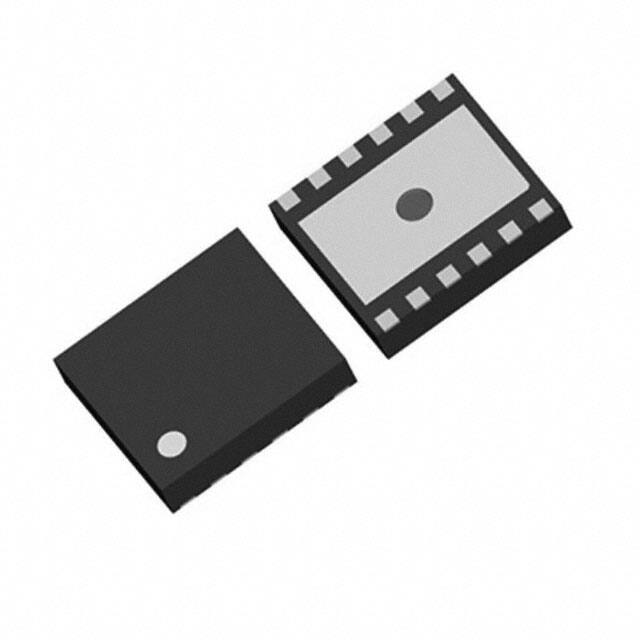
Package ................................................................ DFN(PLP)2730-12
APPLICATION
2
Fixed voltage power supply for portable equipment
Fixed voltage power supply for AMOLED, LCD
�R1286K
NO.EA-283-191114
SELECTION GUIDE
The inverting output voltage (VOUTN), the positive output voltage (VOUTP) and the versions of the inverting output
voltage are user-selectable options.
Product Name
Package
Quantity per Reel
Pb Free
Halogen Free
R1286K$xx∗-TR
DFN(PLP)2730-12
5,000pcs
Yes
Yes
$: Specify the delay time for timer latch (1).
(0) Typ.16msec
(1) Typ.40msec
xx: Specify the set output voltages (VSET) for default value of VOUTx and VONDEF(2)
∗ : Specify setting methods for VOUTN and VOUTP.
VONDEF:VOUTN default value(3) (Internal fixed value at shipping)
VONMIN:VOUTN minimum value with S-Wire
VONMAX:VOUTN maximum value with S-Wire
tTRA:Variable time per 0.1V with S-Wire (4)
∗
A
B
C
D
E
F
G
H
J
K
L
M
N
(1)
(2)
(3)
(4)
(5)
Designation for Settings of VOUTx
VOUTP / VOUTN Fixed Output Voltage type( 5)
VOUTP / VOUTN Adjustable Output Voltage type
VOUTP / VOUTN Fixed Output Voltage type
VONDEF
-5.4 V to -2.4 V
-5.0 V to -2.4 V
-5.2 V to -2.4 V
-5.6 V to -2.6 V
-5.8 V to -2.8 V
-6.0 V to -3.0 V
-5.0 V to -2.4 V
-5.4 V to -2.4 V
-5.6 V to -2.6 V
-5.8 V to -2.8 V
-6.0 V to -3.0 V
-5.2 V to -2.4 V
VONMIN
-5.4 V
-5.0 V
-5.2 V
-5.6 V
-5.8 V
-6.0 V
-5.0 V
-5.4 V
-5.6 V
-5.8 V
-6.0 V
-5.2 V
VONMAX
-2.4 V
-2.0 V
-2.2 V
-2.6 V
-2.8 V
-3.0 V
-2.0 V
-2.4 V
-2.6 V
-2.8 V
-3.0 V
-2.2 V
tTRA
10 ms
10 ms
10 ms
10 ms
10 ms
10 ms
360 µs
360 µs
360 µs
360 µs
360 µs
360 µs
Fixed Output Voltage type only can select the delay time of 40 msec (Typ).
Refer to Voltage Combination List for details.
Selectable in 0.1V step
Refer to the TIMING CHART of S-Wire for details.
Dynamically adjustable output voltage with S-Wire
3
�R1286K
NO.EA-283-191114
Output voltage combination list
VSET codes (xx)
4
VOUTP
VONDEF
01
Setting by external resistor
Setting by external resistor
02
4.6 V
-4.9 V
03
5.8 V
-6.0 V
04
4.8 V
-4.9 V
05
5.4 V
-5.4 V
06
5.0 V
-5.0 V
07
5.0 V
-3.5 V
08
5.6 V
-5.6 V
09
5.8 V
-5.8 V
10
5.5 V
-5.5 V
11
4.6 V
-4.4 V
�R1286K
NO.EA-283-191114
BLOCK DIAGRAMS
R1286KxxxX(1) (Fixed Output Voltage Type)
PVCC
Current
Sense
Current
Sense
Maxduty
Limit
Limit
PGND
PWM
Control
PWM
Control
Timer
LXN
LXP
Short
Protect
Discharge
Control
VOUTN
Q
Q
R S
S R
VOUTNS
Discharge
Control
VOUTP
VOUTPS
Osc
Slope
∑
CE
∑
Soft Start2
Current sense
Vref2
Sequence
Control
S-Wire
Control
Current sense
Soft Start1
Vref1
UVLO
TST
VCC
GND
R1286KxxxX Block Diagram
(1)
X : A to N (Provided, except “B” and “I”)
5
�R1286K
NO.EA-283-191114
R1286K001B (Adjustable Output Voltage Type)
PVCC
Current
Sense
Current
Sense
Maxduty
Limit
Limit
PGND
PWM
Control
PWM
Control
Timer
LXN
LXP
Short
Protect
Discharge
Control
VOUTN
Q
Q
R S
S R
VFBN
Slope
CE
Soft Start2
Current sense
Vref2
Sequence
Control
Enable
Control
∑
Current sense
Soft Start1
Vref1
UVLO
VCC
GND
R1286K001B Block Diagram
6
VOUTP
VFBP
Osc
∑
VREF
Discharge
Control
�R1286K
NO.EA-283-191114
PIN DESCRIPTION
Top View
12 11 10 9
8
Bottom View
7
7
8
9 10 11 12
∗
1
2
3
4
5
6
6
5
4
3
2
1
R1286K (DFN(PLP)2730-12) Pin Configuration
R1286K Pin Description
Symbol
Pin
No. R1286KxxxX( 1) R1286K001B
Description
1
VOUTNS
VFBN
Feed Back Pin for Inverting DC/DC
2
VOUTN
VOUTN
3
LXN
LXN
4
PVCC
PVCC
5
VCC
VCC
Analog Power Input Pin
6
GND
GND
Analog GND Pin
7
PGND
PGND
Power GND Pin
8
LXP
LXP
9
VOUTP
VOUTP
10
VOUTPS
VFBP
11
CE
CE
12
TST
VREF
Outout Pin for Inverting DC/DC
Switching Pin for Inverting DC/DC
Power Input Pin
Switching Pin for Step up DC/DC
Output Pin for Step up DC/DC
Feed Back Pin for Step up DC/DC
Chip Enable and S-Wire Control Input Pin (R1286KxxxX)
Chip Enable Pin (R1286KxxxB)
TEST Pin (2) (R1286KxxxX)
Reference Voltage Output Pin for Inverting DC/DC (R1286KxxxB)
∗ The tab on the bottom of the package is substrate level (GND). It is recommended that the tab be connected to the
ground plane on the board.
(1)
X : A to N (Provided, except “B” and “I”)
(2)
TEST pin must be connected to the GND or leaving it open.
7
�R1286K
NO.EA-283-191114
ABSOLUTE MAXIMUM RATINGS
Symbol
Parameter
(GND = PGND = 0 V)
Rating
Unit
VCC
VCC / PVCC Pin Voltage
-0.3 to 6.0
V
VCE
CE Pin Voltage
-0.3 to 6.0
V
VLXP
LXP Pin Voltage
-0.3 to 6.5
V
VOUTP Pin Voltage
-0.3 to 6.5
V
VCC - 14 to VCC + 0.3
V
VCC - 14 to 0.3
V
VOUTP(S)
VLXN
VOUTN(S)
LXN Pin Voltage
VOUTN Pin Voltage
VTST
TST Pin Voltage [R1286kxxxx(1)]
-0.3 to 6.0
V
VFBP
VFBP Pin Voltage [R1286K001B]
-0.3 to 6.0
V
VFBN
VFBN Pin Voltage [R1286K001B]
-0.3 to VCC + 0.3
V
VREF
VREF Pin Voltage [R1286K001B]
-0.3 to VCC + 0.3
V
3100
mW
PD
Power Dissipation (2) (DFN(PLP)2730-12, JEDEC STD. 51-7)
Tj
Junction Temperature Range
−40 to 125
°C
Tstg
Storage Temperature Range
-55 to 125
ºC
ABSOLUTE MAXIMUM RATINGS
Electronic and mechanical stress momentarily exceeded absolute maximum ratings may cause the permanent
damages and may degrade the lifetime and safety for both device and system using the device in the field. The
functional operation at or over these absolute maximum ratings is not assured.
RECOMMENDED OPERATING CONDITIONS
Symbol
Parameter
Rating
Unit
VCC
Operating Input Voltage
2.3 to 5.5
V
Ta
Operating Temperature Range
−40 to 85
°C
RECOMMENDED OPERATING CONDITIONS
All of electronic equipment should be designed that the mounted semiconductor devices operate within the
recommended operating conditions. The semiconductor devices cannot operate normally over the recommended
operating conditions, even if when they are used over such conditions by momentary electronic noise or surge. And
the semiconductor devices may receive serious damage when they continue to operate over the recommended
operating conditions.
(1)
(2)
8
X : A to N (Provided, except “B” and “I”)
Refer to POWER DISSIPATION for detailed information.
�R1286K
NO.EA-283-191114
ELECTRICAL CHARACTERISTICS
The specifications surrounded by
are guaranteed by Design Engineering at - 40ºC ≤ Ta ≤ 85ºC.
R1286K Electrical Characteristics
(Ta = 25ºC)
Symbol
Parameter
Conditions
Min.
ICC
VCC Consumption Current
(at no switching)
VCC=5.5V
1.2
ISTANDBY
Standby Current
VCC=VLXP=5.5V , VCE=VLXN=0V
0.1
5
µA
VUVLO1
UVLO Detection Voltage
Falling
2.05
2.15
V
VUVLO2
UVLO Release Voltage
Rising
VUVLO1
+0.10
2.28
V
fOSC
Oscillator Frequency
VCC=3.7V
1500
1750
2000
kHz
VCEH
CE Pin Input Voltage, high
VCC=5.5V
1.2
VCEL
CE Pin Input Voltage, low
VCC=2.3V
RCE
CE Pin Pull-down
Resistance
VCC=3.7V
160
kΩ
TTSD
Thermal Shutdown
Detection Temperature
VIN=3.7V
150
°C
TTSR
Thermal Shutdown
Release Temperature
VIN=3.7V
125
°C
1.95
Typ.
Max.
Unit
mA
V
0.4
V
[ R1286K0xxx]
tDLY
Delay Time for Protection
VCC=3.7V
8
16
24
ms
VCC=3.7V
32
40
48
ms
[ R1286K1xxX( 1)]
tDLY
Delay Time for Protection
■ Set-up DC/DC Converter (CH1)
Maxduty1 Maximum Duty Cycle 1
VCC=3.7V
85
%
VOUTP Discharge Current
VCC=3.7V, VOUTP=0.1V
1.1
mA
tSSP
CH1 Soft-start Time
VCC=3.7V
RLXP
LXP Pin On-resistance
VCC=3.7V
400
mΩ
Synchronous SW Pch.Onresistance
VCC=3.7V
700
mΩ
VCC=3.7V
1.0
A
VCC=3.7V
1.1
A
IVOUTP
RSYNCP
1.6
2.4
3.0
ms
[ R1286K0xxx]
ILIMLXP
LXP Pin Limit Current
[ R1286K1xxX]
ILIMLXP
LXP Pin Limit Current
[ R1286KxxxX]
VOUTP
(1)
VOUTP Voltage Tolerance
VCC=3.7V
×0.991
VSET
×1.009
V
X : A to N (Provided, except “B” and “I”)
9
�R1286K
NO.EA-283-191114
The specifications surrounded by
are guaranteed by Design Engineering at - 40ºC ≤ Ta ≤ 85ºC.
R1286K Electrical Characteristics (Continued)
Symbol
Parameter
(Ta = 25ºC)
Conditions
Min.
Typ.
Max.
Unit
0.985
1.000
1.015
V
0.1
µA
[ R1286K001B]
VFBP
VFBP Voltage Tolerance
VCC=3.7V
IFBP
VFBP Input Current
VCC=5.5V, VFBP=0V or 5.5V
-0.1
■ Inverting DC/DC Converter (CH2)
Maxduty2 Maximum Duty Cycle 2
VCC=3.7V
90
%
IVOUTN
VOUTN Discharge Current
VCC=3.7V, VOUTN=-0.1
0.3
mA
RLXN
LXN Pin On-resistance
VCC=3.7V
400
mΩ
Synchronous SW Nch.Onresistance
VCC=3.7V
600
mΩ
VCC=3.7V
1.5
A
VCC=3.7V
1.8
A
RSYNCN
[ R1286K0xxx]
ILIMLXN
LXN Pin Limit Current
[ R1286K1xxX]
ILIMLXN
LXN Pin Limit Current
[ R1286KxxxX]
VONDEF
VOUTN Default Voltage
Tolerance
VCC=3.7V, selectable between
VONMIN and VONMAX at shipping
VSET
-70
VSET
VSET
+70
mV
VONMIN
VOUTN Minimum Voltage
Tolerance
VCC=3.7V, selectable between
-2.0V and -3.0V at shipping
VSET
-70
VSET
VSET
+70
mV
VONMAX
VOUTN Maximum Voltage
Tolerance
VCC=3.7V
VSET
-70
VONMIN
+ 3.0V
VSET
+70
mV
VOUTN
VOUTN Voltage Tolerance
(S-Wire)
VCC=3.7V
(Guaranteed by design
engineering)
VSET
-80
VSET
VSET
+80
mV
tSSN
Soft-start Time for CH2
VCC=3.7V
1.6x
VONDEF/
-4.9
2.3x
VONDEF/
-4.9
3.0x
VONDEF/
-4.9
ms
[ R1286K001B]
VFBN
VFBN Voltage Tolerance
VCC=3.7V
-25
0
25
mV
VREF
VREF Voltage Tolerance
VCC=3.7V
1.18
+VFBN
1.2
+VFBN
1.22
+VFBN
V
IFBN
VFBN Input Current
VCC=5.5V, VFBN = 0V or 5.5V
-0.1
0.1
µA
tSSN
Soft-start Time for CH2
VCC=3.7V
1.6
3.6
ms
2.8
All test items listed under Electrical Characteristics are done under the pulse load condition (Tj≈Ta=25ºC).
10
�R1286K
NO.EA-283-191114
THEORY OF OPERATION
Start-up Sequence
When CE level turns from ‘L’ to ‘H’ level, the softstart of CH1 starts the operation. After detecting output voltage
of CH1(VOUTP)as the nominal level, the soft start of CH2 starts the operation.
CE
CH1 (VOUTP)
0V
Soft start CH1
Soft Start CH2
CH2 (VOUTN)
Auto Discharge Function
When CE level turns from ‘H’ to ‘L’ level, the R1286K goes into standby mode and switching of the outputs of
LXP and LXN will stop. Then dischage switsh between VOUTN and GND and switch between VOUTP and GND turn
on and discharge the negative output voltage and positive output voltage. The positive and negative output
voltage is discharged to 0V in standby mode. If Vcc voltage became lower than UVLO detect voltage ,
discharge switches also turn on and discharge output voltage(VOUTN and VOUTP) .
In case of timer latch protection,discharge switches will keep off .
CE
VOUTP
0V
VOUTN
Discharge
Thermal Shutdown Protection
If the over temparature is detected, internal Mosfet will turn-off soon. And when the temparature get lower than
the release temparature, IC is reset and restart the operation.
11
�R1286K
NO.EA-283-191114
Overcurrent Protection and Short-circuit Protection Circuit Timer
The over current protection circuit supervises the peak current of the inductor (The current passing through
NMOS transistor of CH1 and PMOS transistor of CH2) with respect to each switching cycle. If the peak current
exceeds the LX current limit (ILIMLXP or ILIMLXN), the over current protection circuit turns off the NMOS transistor
of CH1 or PMOS transistor of CH2. If the over current continues more than the protection delay time (TDLY),
the short current protection circuit latches the built-in driver at OFF state and stops the operation of DC/DC
converter.
∗ LX limit current (ILIMLXP or ILIMLXN) and the protection delay time (TDLY) can be easily affected by self-heating
and ambient environment. The drastic drop of output voltage or the unstable output voltage caused by the
short-circuiting may affect the protection operation and the delay time.
To release the latch over current protection, reset the IC by inputting “L” into CE pin or by making the input
voltage lower than the UVLO detector threshold (VUVL01).
During the softstart operation of CH1 and CH2, the timer operates until detecting output voltage of CH2 (VOUTN)
as the nominal level. Therefore, even if the softstart cannot finish correctly because of the short circuit, the
protection timer function will be able to work correctly.
Sequence with S-Wire Control for VOUTN (R1286KxxxX(1))
Adjusted Value
Adjusted Value
Setting Command Setting Command
S-Wire Input
to CE pin
VOUTP
Output
Voltage
VOUTN
tSS
Shutdown
tstop ttra
Default Value
tstop ttra
Adjusted Value
toff_dly
Adjusted Value
■ Default Value Driving
VOUTP rises up first and secondarily VOUTN goes down. In this time VOUTN is set VONDEF.
Soft-start time (tSS) =2.4ms + 2.3 x VONDEF/ -4.9 (Typ.)
(1)
X : A to N (Provided, except “B” and “I”)
12
tvo_off
Shutdown
�R1286K
NO.EA-283-191114
■ Adjusted Value Driving
After receiving the adjusted value setting command, VOUTN is changed to the target voltage in multiple steps
method. Adjusted value is also selectable with pulse count (Please refer to VOUTN VARIABLE TABLE).
In the case of R1286KxxxA/C/D/E/F/G,
VOUTN change 0.01V step in every 1ms and it takes 10ms per 0.1V that is minimum step for VOUTN setting value.
In the case of R1286KxxxH/J/K/L/M/N,
VOUTN change 0.01V step in every 36us and it takes 360us per 0.1V that is minimum step for VOUTN setting value.
[Multiple steps method (In case of ΔVOUT = 0.1V)]
Adjusted Value Setting Command
S-Wire
VOUTN
0.01V
tSTOP
0.1V
1ms
or 36µs
ttra
・Multiple step rate : 0.01V / 1ms or 36µs
・Transient time (ttra) for minimum ΔVOUTN : 10 ms or 0.36 ms
13
�R1286K
NO.EA-283-191114
VOUTN Variable Table
The adjusted value setting command are operated with S-Wire input (pulse count) as the following table.
VOUTN Variable Table (31 steps)
BIT
R1286KxxxA
R1286KxxxG
0 (Default)
-2.4 to -5.4
-3.0 to -6.0
1
-5.4
-6.0
2
-5.3
-5.9
3
-5.2
-5.8
4
-5.1
-5.7
5
-5.0
-5.6
6
-4.9
-5.5
7
-4.8
-5.4
8
-4.7
-5.3
9
-4.6
-5.2
10
-4.5
-5.1
11
-4.4
-5.0
12
-4.3
-4.9
13
-4.2
-4.8
14
-4.1
-4.7
15
-4.0
-4.6
16
-3.9
-4.5
17
-3.8
-4.4
18
-3.7
-4.3
19
-3.6
-4.2
20
-3.5
-4.1
21
-3.4
-4.0
22
-3.3
-3.9
23
-3.2
-3.8
24
-3.1
-3.7
25
-3.0
-3.6
26
-2.9
-3.5
27
-2.8
-3.4
28
-2.7
-3.3
29
-2.6
-3.2
30
-2.5
-3.1
31
-2.4
-3.0
(Pulse Count)
14
�R1286K
NO.EA-283-191114
Timing Chart for Commands with S-Wire
VIH
VIL
ton
Timing specification
Item
Symbol
toff
tstop
Min.
Typ.
70
tssp + tssn
10
(R1286KxxxA/C/D/E/F/G)
0.36
(R1286KxxxH/J/K/L/M/N)
90
Soft-start time
tss
VOUTN Transient time (1 step)
ttra
Turn-off delay time
toff_dly
VOUT discharge time
tvo_off
CE pin input voltage, high
VIH
CE pin input voltage, low
VIL
S-Wire time, high
ton
2
S-Wire time, low
toff
S-Wire command stop time
tstop
Max.
Unit
ms
ms
110
2.0
1.2
µs
ms
V
0.4
V
10
20
µs
2
10
20
µs
70
90
110
µs
15
�R1286K
NO.EA-283-191114
Operation of Set-up DC/DC Converter (CH1) and Output Current
IL2
Inductor
VIN
Pch Tr
IOUT
VOUT
IL1
Nch Tr
CL
Basic Circuit
ILxmax
IL
IL
ILxmax
ILxmin
ILxmin
Tf
t
ton
toff
T=1/fosc
Discontinuous Inductor Current Mode
t
ton
T=1/fosc
toff
Continuous Inductor Current Mode
Inductor Current Waveforms (IL) through Indictor (L)
The PWM control type of CH1 has two operation modes characterized by the continuity of inductor current:
discontinuous inductor current mode and continuous inductor current mode.
When a NMOS Tr. is in On-state, the voltage to be applied to the inductor (L) is described as VIN. An increase
in the inductor current (IL1) can be written as follows:
IL1 = VIN x ton / L ·········································································································· Equation 1
In the CH1 circuit, the energy accumulated during the On-state is transferred into the capacitor even in the Offstate. A decrease in the inductor current (IL2) can be written as follows:
IL2 = (VOUT − VIN) x tf / L ································································································· Equation 2
16
�R1286K
NO.EA-283-191114
In the PWM control, IL1 and IL2 become continuous when tf = toff, which is called continuous inductor current
mode. When the device is in continuous inductor current mode and operates in steady-state conditions, the
variations of IL1 and IL2 are same:
VIN x ton / L = (VOUT − VIN) x toff / L ··················································································· Equation 3
Therefore, the duty cycle in continuous inductor current mode is:
Duty = ton / (ton + toff) = (VOUT − VIN) / VOUT ········································································ Equation 4
If the input voltage (VIN) is equal to VOUT, the output current (IOUT) is:
IOUT = VIN2 x ton / (2 x L x VOUT) ························································································ Equation 5
If IOUT is larger than Equation 5, the device switches to continuous inductor current mode. The LX peak current
flowing through L (ILxmax) is:
ILxmax = IOUT x VOUT / VIN + VIN x ton / (2 x L) ······································································ Equation 6
ILxmax = IOUT x VOUT / VIN + VIN x T x (VOUT − VIN) / (2 x L x VOUT) ············································· Equation 7
The LX peak current limit circuit operates in both modes if the ILxmax becomes more than the LX peak current
limit. When considering the input and output conditions or selecting the external components, please pay
attention to ILxmax.
Notes: The above calculations are based on the ideal operation of the device. They do not include the losses
caused by the external components or LX switch. The actual maximum output current will be 70% to 90% of
the above calculation results. Especially, if IL is large or VIN is low, it may cause the switching losses.
17
�R1286K
NO.EA-283-191114
Operation of Inverting DC/DC Converter (CH2) and Output Current
Pch Tr
Nch Tr
IOUT
VOUT
VIN
IL1
IL2
CL
Inductor
Basic Circuit
Discontinuous Inductor Current Mode
Continuous Inductor Current Mode
ILxmax
IL
IL
ILxmax
ILxmin
ILxmin
tf
t
ton
toff
T=1/fosc
t
ton
toff
T=1/fosc
Inductor Current Waveforms (IL) through Indictor (L)
The PWM control type of CH2 has two operation modes characterized by the continuity of inductor current:
discontinuous inductor current mode and continuous inductor current mode.
When a PMOS Tr. is in ON-state, the voltage to be applied to the inductor (L) is described as V . An increase
IN
in the inductor current (IL1) can be written as follows:
IL1 = VIN x ton / L ·········································································································· Equation 8
In the CH2 circuit, the energy accumulated during the On-state is transferred into the capacitor even in the Offstate. A decrease in the inductor current (IL2) can be written as follows:
IL2 = |VOUT| x tf / L ········································································································· Equation 9
18
�R1286K
NO.EA-283-191114
In the PWM control type, when tf = toff, the inductor current will be continuous and the operation of CH2 will
be continuous inductor current mode. When the device is in continuous inductor current mode and operates
in steady-state conditions, the variation of IL1 and IL2 are same:
VIN x ton / L = |VOUT| x toff / L ························································································· Equation 10
Therefore, the duty cycle in continuous inductor current mode is:
Duty = ton / (ton + toff) = |VOUT| / (|VOUT| + VIN) ··································································· Equation 11
If the input voltage (VIN) equal to VOUT, the output current (IOUT) is:
IOUT = VIN2 x ton / (2 x L x |VOUT|) ····················································································· Equation 12
If IOUT is larger than Equation 12, the device switches to continuous inductor current mode. The LX peak current
flowing through L (ILxmax) is:
ILxmax = IOUT x (|VOUT| + VIN) / VIN + VIN x ton / (2 x L) ························································· Equation 13
ILxmax = IOUT x (|VOUT| + VIN) / VIN + VIN x |VOUT| x T / { 2 x L x (|VOUT| + VIN) } ··························· Equation 14
The LX peak current limit circuit operates in both modes if the ILxmax becomes more than the LX peak current
limit. When considering the input and output conditions or selecting the external components, please pay
attention to ILxmax.
Notes: The above calculations are based on the ideal operation of the device. They do not include the losses
caused by the external components or LX switch. The actual maximum output current will be 70% to 90% of
the above calculation results. Especially, if IL is large or VIN is low, it may cause the switching losses.
19
�R1286K
NO.EA-283-191114
APPLICATION INFORMATION
Typical Application Circuits
VOUTN
VOUTNS
C2
VOUTN
TST
EN Control
S-Wire Control
CE
L2
LXN
VOUTPS
VOUTP
PVCC
VOUTP
L1
C1
VCC
LXP
GND
PGND
C3
R1286KxxxX (Fixed Output Voltage Type) Typical Application Circuit
C4
R4
VOUTN
R5
VFB
C2
L2
VOUTN
LXN
PVCC
C1
EN Control
VREF
CE
R1
VFBP
VOUTP
VCC
LXP
GND
PGND
C5
R3
R2
L1
VOUTP
C3
R1286K001B (Adjustable Output Voltage Type) Typical application Circuit
Recommended External Components
Symbol
Description
L1
VLF302510M-4R7M (TDK)、VLF3010S-4R7M (TDK)
L2
VLF4012S-4R7M (TDK)、NR4012T4R7M (TAIYOYUDEN)
C1(CIN), C2(COUTN), C3(COUTP)
4.7µF、 2012size X5R T=0.85max
C4 (CREF)(1)
0.1µF、 0603size
(1)
R1286K001B Only
20
�R1286K
NO.EA-283-191114
Precautions for Selecting External Components
Place a ceramic capacitor of 4.7µF or more (C1) between VCC pin/PVCC pin and GND pin/ PGND pin.
Place a ceramic capacitor of 4.7µF or more (C2, C3) between VOUTP pin / VOUTN pin and GND.
Place a ceramic capacitor of 0.1µF to 2.2µF (C4) between VREF pin and GND. [ R1286K001B ]
Step-up DC/DC Converter Output Voltage Setting [ R1286K001B ]
The output voltage VOUTP of the step-up DC/DC converter is controlled with maintaining the VFBP as 1.0V.
VOUTP can be set with adjusting the values of R1 and R2 as in the next formula.
VOUTP = VFBP × (R1 + R2) / R1
VOUTP can be set from 4.6V to 5.8V. The appropriate value range of R1 is from 20kΩ to 60k Ω.
Inverting DC/DC Converter Output Voltage Setting [ R1286K001B ]
The output voltage VOUTN of the inverting DC/DC converter is controlled with maintaining the VFBN as 0V.
VOUTN can be set with adjusting the values of R1 and R2 as in the next formula.
VOUTN = VFBN - (VREF - VFBN) × R5 / R4
VOUTN can be set from -2.0V to -6.0V. The appropriate value range of R4 is from 2.5kΩ to 60kΩ.
Phase Compensation of Step-up DC/DC Converter [ R1286K001B ]
DC/DC converter’s phase may lose 180 degree by external components of L and C and load current.
Because of this, the phase margin of the system will be less and the stability will be worse. Therefore, the
phase must be gained.
Zero will be formed with R1 and C5.
C5 [pF] = 300 / R1 [kΩ]
If the noise of the system is large, the output noise affects the feedback and the operation may be unstable.
In that case, another resistor R3 will be set. The appropriate value range is from 10Ω to 1kΩ.
21
�R1286K
NO.EA-283-191114
TECHNICAL NOTES
The performance of a power source circuit using this device is highly dependent on a peripheral circuit. A
peripheral component or the device mounted on PCB should not exceed a rated voltage, a rated current or a
rated power. When designing a peripheral circuit, please be fully aware of the following points.
Wire the bypass capacitor (C1) between the VCC pin, the GND pin, or the PVCC pin as short as possible.
The GND pin should be connected to the GND plane of the PCB.
Wire the GND of the output capacitors (C2, C3) to the GND pin of the device as short as possible.
The wiring among each GND line of C1, C2, and C3 and the GND pin of the device must be short as
possible via the device.
The wiring between LXP pin, LXN pin and inductor each should be as short as possible and mount output
capacitors (C2 and C3) as close as possible to the VOUTP, VOUTN each.
Input impedance of VOUTPS pin, VOUTNS pin, VFBP pin, and VFBN pin is high, therefore, the external noise
may affect the performance. The coupling capacitance between these nodes and switching lines must be
as short as possible.
As shown in the diagrams of the current paths of boost DC/DC converter and the current path of inverting
DC/DC converter, the parasitic impedance, inductance, and the capacitance in the parts pointed with red
arrows have an influence against the stability of the DC/DC converters and become a cause of the noise.
Therefore, such parasitic elements must be made as small as possible. Wiring of the current paths must
be short and thick.
【Set-up DCDC】
NMOSFET-ON
PMOSFET-ON
【Inverting DCDC】
PMOSFET-ON
22
NMOSFET-ON
�R1286K
NO.EA-283-191114
PCB Layout
R1286K Board Layout [PKG: DNF (PLP) 2730-12]
Top Layer
Back Layer
R1286KxxxX( 1)(Fixed Output Voltage Type)Board Layout
Top Layer
Back Layer
R1286K001B (Adjustable Output Voltage Type) Board Layout
(1)
X : A to N (Provided, except “B” and “I”)
23
�R1286K
NO.EA-283-191114
TYPICAL CHARACTERISTICS
Typical Characteristics are intended to be used as reference data, they are not guaranteed.
1) Output Voltage vs. Output Current
R1286KxxxX(1) (VOUTP = 4.6 V)
R1286KxxxX (VOUTP = 5.4 V)
(Ta = 25°C)
4.7
5.5
4.68
5.48
4.66
5.46
4.64
5.44
4.62
5.42
VOUT P[V]
VOUT P[V]
(Ta = 25°C)
4.6
4.58
4.56
Vin= 4.8 V
Vin= 3.7 V
Vin= 2.9 V
4.54
4.52
5.4
5.38
5.36
Vin= 4.8 V
Vin= 3.7 V
Vin= 2.9 V
5.34
5.32
5.3
4.5
0
0
25 50 75 100 125 150 175 200 225 250 275 300
25 50 75 100 125 150 175 200 225 250 275 300
IOUT P [mA]
IOUT P [mA]
R1286KxxxX (VOUTP = 5.8 V)
R1286KxxxX (VOUTN = -4.9 V)
(Ta = 25°C)
5.9
-4.8
5.88
-4.82
5.86
-4.84
5.84
-4.86
5.82
-4.88
VOUT N[V]
VOUT P[V]
(Ta = 25°C)
5.8
5.78
-4.9
-4.92
5.76
Vin= 4.8 V
Vin= 3.7 V
Vin= 2.9 V
5.74
5.72
-4.94
-4.98
5.7
0
-5
25 50 75 100 125 150 175 200 225 250 275 300
0
IOUT P [mA]
R1286KxxxX (VOUTN = -5.4 V)
Vin= 4.8 V
Vin= 3.7 V
Vin= 2.9 V
-4.96
25 50 75 100 125 150 175 200 225 250 275 300
IOUT N [mA]
R1286KxxxX (VOUTN = -6.0 V)
-5.32
-5.92
-5.34
-5.94
-5.36
-5.96
-5.38
-5.98
-5.4
-5.42
-5.44
Vin= 4.8 V
Vin= 3.7 V
Vin= 2.9 V
-5.48
-5.5
0
25 50 75 100 125 150 175 200 225 250 275 300
IOUT N [mA]
24
-6
-6.02
-5.46
(1)X
(Ta = 25°C)
-5.9
VOUT N[V]
VOUT N[V]
(Ta = 25°C)
-5.3
: A to N (Provided, except “B” and “I”)
-6.04
Vin= 4.8 V
Vin= 3.7 V
Vin= 2.9 V
-6.06
-6.08
-6.1
0
25 50 75 100 125 150 175 200 225 250 275 300
IOUT N [mA]
�R1286K
NO.EA-283-191114
2) Efficiency vs. Output Current
R1286KxxxX (VOUTP = 4.6 V, VOUTN = -4.9 V)
R1286KxxxX (VOUTP = 5.4 V, VOUTN = -5.4 V)
(Ta = 25°C)
(Ta = 25°C)
100
90
90
80
80
70
Efficiency[%]
Efficiency[%]
100
60
50
40
Vin= 4.2 V
Vin= 3.7 V
Vin= 2.9 V
30
20
0
25 50 75 100 125 150 175 200 225 250 275 300
IOUT = IOUTP = IOUT N[mA]
70
60
50
40
Vin= 4.2 V
Vin= 3.7 V
Vin= 2.9 V
30
20
0
25
50
75 100 125 150 175 200 225 250 275 300
IOUT = IOUTP = IOUT N[mA]
R1286KxxxX (VOUTP = 5.8 V, VOUTN = -6.0 V)
(Ta = 25°C)
100
90
Efficiency[%]
80
70
60
50
Vin= 4.2 V
Vin= 3.7 V
Vin= 2.9 V
40
30
20
0
25 50 75 100 125 150 175 200 225 250 275 300
IOUT = IOUTP = IOUT N[mA]
25
�R1286K
NO.EA-283-191114
3) Turn-on/Turn-off Waveform by CE
R1286Kx02A (VIN=3.7 V, IOUTP = IOUTN = 0 mA )
(Ta = 25°C)
CH1=CE
CH2=VOUTP
CH3=VOUTN
CH4=IIN
CH1=CE
CH2=VOUTP
CH3=VOUTN
CH4=IIN
R1286Kx05A (VIN=3.7 V, IOUTP = IOUTN = 0 mA, COUTP = COUTN = 4.7µF)
(Ta = 25°C)
CH1=CE
CH1=CE
CH2=VOUTN
CH2=VOUTN
CH3=VOUTP
CH3=VOUTP
CH4=IIN
CH4=IIN
R1286Kx05A (VIN=3.7 V, IOUTP = IOUTN = 0 mA, COUTP = 10 µF x 2, COUTN = 4.7µF)
(Ta = 25°C)
26
CH1=CE
CH1=CE
CH2=VOUTN
CH2=VOUTN
CH3=VOUTP
CH3=VOUTP
CH4=IIN
CH4=IIN
�R1286K
NO.EA-283-191114
4) VOUTN Waveform with S-Wire Control
R1286Kx02A
(-4.9 V ≤ VOUTN ≤ -2.4 V, IOUTP = IOUTN = 0 mA )
R1286Kx02A
(-2.4 V ≤ VOUTN ≤ -4.9 V, IOUTP = IOUTN = 0 mA )
(Ta = 25°C)
(Ta = 25°C)
puls
pulse
CH1=CE
CH1=CE
CH2=VOUTN
CH2=VOUTN
CH4=IIN
CH4=IIN
5) Load Transient Response
R1286KxxxX (VOUTP = 4.6 V)
R1286KxxxX (VOUTN = -4.9 V)
(Ta = 25°C)
CH3=VOUTP
CH4=IOUT
6) Line Transient Response
R1286KxxxX (VOUTP = 4.6 V, IOUTP = 100 mA)
(Ta = 25°C)
(Ta = 25°C)
CH3=VOUTN
CH4=IOUT
R1286KxxxX (VOUTN = -4.9 V, IOUTN = 100 mA)
(Ta = 25°C)
CH1=VIN
CH1=VIN
CH3=VOUTP
CH3=VOUTN
27
�R1286K
NO.EA-283-191114
7) UVLO Voltage vs. Temperature
R1286KxxxX
8) VOUTP Voltage vs. Temperature
R1286Kx02X
4.65
2.25
2.2
UVLO Release
VOUTP [V] A
VUVLO [V] A
4.63
2.15
2.1
2.05
UVLO
2
4.61
4.59
4.57
1.95
1.9
4.55
-40
-20
0
20
40
60
80
-40
-20
0
Ta [°C]
9) VOUTN Voltage vs. Temperature
R1286KxxxC
-4.9
-1.97
-4.94
60
80
40
60
80
VOUTN [V] A
VOUTN [V] A
-1.95
-4.98
-2.01
-5.02
-2.03
-5.06
-2.05
-5.1
-40
-20
0
20
40
60
80
R1286KxxxG
-5.85
-5.9
-5.95
-6
-6.05
-6.1
-6.15
-40
-20
0
20
Ta [°C]
-40
-20
0
20
Ta [°C]
Ta [°C]
VOUTN [V] A
40
R1286KxxxX
-1.99
28
20
Ta [°C]
40
60
80
�R1286K
NO.EA-283-191114
10) VFBN Voltage vs. Temperature
R1286K001B
11) VREF Voltage vs. Temperature
R1286K001B
0.02
1.21
0.01
1.2
VREF [V] A
1.22
VFBN [V] A
0.03
0
1.19
-0.01
1.18
-0.02
1.17
-0.03
1.16
-40
-20
0
20
40
60
80
-40
-20
0
Ta [°C]
20
40
60
80
Ta [°C]
12) LXP Current Limit vs. Temperature
R1286KxxxX
13) LXN Limit Current vs. Temperature
R1286KxxxX
2.1
1.4
2
1.3
1.9
1.2
R1286K1xxX
LIMLXN [A] A
LIMLXP [A] A
R1286K1xxX
1.8
1.7
1.1
1.6
R1286K0xxX
1
R1286K0xxX
1.5
1.4
0.9
-40
-20
0
20
40
60
80
Ta [°C]
-40
-20
0
20
40
60
80
Ta [°C]
14) Oscillator Frequency vs. Temperature
R1286KxxxX
FOSC1A [kHz] A
1850
1800
1750
1700
1650
-40
-20
0
20
40
60
80
Ta [°C]
29
�R1286K
NO.EA-283-191114
16) Maxduty2 vs. Temperature
R1286KxxxX
87
94
86
93
Maxduty2 [%] A
Maxduty1 [%] A
15) Maxduty1 vs. Temperature
R1286KxxxX
85
84
83
92
91
90
89
82
88
81
-40
-20
0
20
40
60
-40
80
-20
0
Ta [°C]
17) CH1 Soft-start Time vs. Temperature
R1286KxxxX
40
60
80
18) CH2 Soft-start Time vs. Temperature
R1286KxxxG
2.9
3.4
2.7
3.2
TSS2 [ms] A
TSS1 [ms] A
20
Ta [°C]
2.5
2.3
2.1
3
2.8
2.6
1.9
2.4
-40
-20
0
20
40
60
80
-40
-20
0
Ta [°C]
20
40
60
80
Ta [°C]
19) CH2 Soft-start Time vs. Temperature
R1286K001B
20) Delay Time for Protection vs. Temperature
R1286KxxxX
50
3.3
45
R1286K1xxX
40
TDLY[ms] A
TSS2 [ms] A
3.1
35
2.9
30
2.7
25
R1286K0xxX
20
2.5
15
2.3
10
-40
-20
0
20
Ta [°C]
30
40
60
80
-40
-20
0
20
Ta [°C]
40
60
80
�POWER DISSIPATION
DFN(PLP)2730-12
Ver. A
The power dissipation of the package is dependent on PCB material, layout, and environmental conditions.
The following measurement conditions are based on JEDEC STD. 51-7.
Measurement Conditions
Item
Measurement Conditions
Environment
Mounting on Board (Wind Velocity = 0 m/s)
Board Material
Glass Cloth Epoxy Plastic (Four-Layer Board)
Board Dimensions
76.2 mm × 114.3 mm × 0.8 mm
Copper Ratio
Outer Layer (First Layer): Less than 95% of 50 mm Square
Inner Layers (Second and Third Layers): Approx. 100% of 50 mm Square
Outer Layer (Fourth Layer): Approx. 100% of 50 mm Square
Through-holes
0.3 mm × 23 pcs
Measurement Result
Item
(Ta = 25°C, Tjmax = 125°C)
Measurement Result
Power Dissipation
3100 mW
Thermal Resistance (ja)
ja = 32°C/W
Thermal Characterization Parameter (ψjt)
ψjt = 8°C/W
ja: Junction-to-Ambient Thermal Resistance
ψjt: Junction-to-Top Thermal Characterization Parameter
Power Dissipation vs. Ambient Temperature
Measurement Board Pattern
i
�PACKAGE DIMENSIONS
DFN(PLP)2730-12
DM-DFN(PNP)2730-12-JE-B
DFN(PLP)2730-12 Package Dimensions (Unit: mm)
i
�1. The products and the product specifications described in this document are subject to change or discontinuation of
production without notice for reasons such as improvement. Therefore, before deciding to use the products, please
refer to Ricoh sales representatives for the latest information thereon.
2. The materials in this document may not be copied or otherwise reproduced in whole or in part without prior written
consent of Ricoh.
3. Please be sure to take any necessary formalities under relevant laws or regulations before exporting or otherwise
taking out of your country the products or the technical information described herein.
4. The technical information described in this document shows typical characteristics of and example application circuits
for the products. The release of such information is not to be construed as a warranty of or a grant of license under
Ricoh's or any third party's intellectual property rights or any other rights.
5. The products listed in this document are intended and designed for use as general electronic components in standard
applications (office equipment, telecommunication equipment, measuring instruments, consumer electronic products,
amusement equipment etc.). Those customers intending to use a product in an application requiring extreme quality
and reliability, for example, in a highly specific application where the failure or misoperation of the product could result
in human injury or death (aircraft, spacevehicle, nuclear reactor control system, traffic control system, automotive and
transportation equipment, combustion equipment, safety devices, life support system etc.) should first contact us.
6. We are making our continuous effort to improve the quality and reliability of our products, but semiconductor products
are likely to fail with certain probability. In order to prevent any injury to persons or damages to property resulting from
such failure, customers should be careful enough to incorporate safety measures in their design, such as redundancy
feature, fire containment feature and fail-safe feature. We do not assume any liability or responsibility for any loss or
damage arising from misuse or inappropriate use of the products.
7. Anti-radiation design is not implemented in the products described in this document.
8. The X-ray exposure can influence functions and characteristics of the products. Confirm the product functions and
characteristics in the evaluation stage.
9. WLCSP products should be used in light shielded environments. The light exposure can influence functions and
characteristics of the products under operation or storage.
10. There can be variation in the marking when different AOI (Automated Optical Inspection) equipment is used. In the
case of recognizing the marking characteristic with AOI, please contact Ricoh sales or our distributor before attempting
to use AOI.
11. Please contact Ricoh sales representatives should you have any questions or comments concerning the products or
the technical information.
Halogen Free
Ricoh is committed to reducing the environmental loading materials in electrical devices
with a view to contributing to the protection of human health and the environment.
Ricoh has been providing RoHS compliant products since April 1, 2006 and Halogen-free products since
April 1, 2012.
Official website
https://www.e-devices.ricoh.co.jp/en/
Contact us
https://www.e-devices.ricoh.co.jp/en/support/
�