R1501x SERIES
1A LDO REGULATOR (Operating Voltage up to 24V)
NO.EA-184-160801
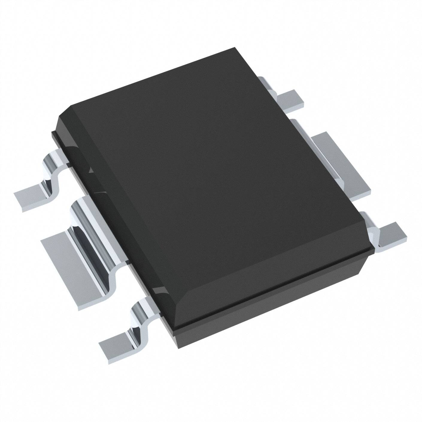
OUTLINE
The R1501x series are CMOS-based positive voltage regulator (VR) ICs. The R1501xxxxB has features of high
input voltage operating, 1A output current drive, and low supply current.
A DMOS transistor is used for the driver, high voltage operating and low on resistance (0.6Ω at VOUT=10V) device
is realized. A standard regulator circuit with a current limit circuit and a thermal shutdown circuit are built in the
R1501x series.
As the operating temperature range is from -40°C to 105°C and maximum input voltage is up to 24V, the R1501x
series are suitable for the constant voltage source for digital home appliances and car accessories.
The regulator output voltage is fixed in the R1501x. Output voltage accuracy is ±2.0% and output voltage range
is from 3.0V to 12.0V with a step of 0.1V, and from 12.5V to 18.0V with a step of 0.5V. The chip enable pin realizes
ultra low supply current standby mode.
Since the packages for these ICs are the HSOP-6J for high density mounting of the ICs on boards, and the TO252-5-P2.
∗) The DMOS (Double Diffused MOS) transistor adopted by R1501x is characterized by a double diffusion structure which
comprises a low density n-type (channel) diffused layer and a high density p-type (sources) diffused layer from the edge
of the gate electrode. The R1501x series possess outstanding properties of high operating voltage and low on-resistance,
which have been achieved by the channel length scaled down to submicron dimensions and decreased thickness of the
gate oxide film.
FEATURES
•
•
•
•
•
•
•
•
•
•
•
•
•
•
Supply Current ............................................................. Typ. 70µA
Standby Current ........................................................... Typ. 0.1µA
Output Current.............................................................. Min. 1A
Input Voltage Range ................................................... 3.0V to 24.0V
Ripple Rejection ......................................................... Typ. 60dB (VSET=5.0V)
Output Voltage Range .................................................. 3.0V to 12.0V (0.1V steps)
12.5V to 18.0V (0.5V steps)
(For other voltages, please refer to MARK INFORMATIONS.)
Output Voltage Accuracy .............................................. ±2%
Temperature-Drift Coefficient of Output Voltage .......... Typ. ±100ppm/°C
Line Regulation ............................................................ Typ. 0.05%/V
Packages...................................................................... HSOP-6J, TO-252-5-P2
Operating Temperature range ...................................... −40°C to 105°C
Built-in Current Limit Circuit
Built-in Fold-Back Circuit
Built-in Thermal Shutdown Circuit
APPLICATIONS
•
•
•
•
Power source for home appliances such as refrigerators, rice cookers, electric water warmers, etc.
Power source for car audio equipment, car navigation system, ETC system, etc.
Power source for notebook PCs, digital TVs, cordless phones, and private LAN system, etc.
Power source for office equipment machines such as copiers, printers, facsimiles, scanners, projectors, etc.
1
�R1501x
NO.EA-184-160801
BLOCK DIAGRAMS
R1501xxxxB
Thermal Shutdown
Circuit
VDD
VOUT
Vref
Short
Protection Current Limit
CE
GND
SELECTION GUIDE
The output voltage, package, etc. for the ICs can be selected at the user’s request.
Product Name
Package
Quantity per Reel
Pb Free
Halogen Free
R1501SxxxB-E2-FE
HSOP-6J
1,000 pcs
Yes
Yes
R1501JxxxB-T1-FE
TO-252-5-P2
3,000 pcs
Yes
Yes
xxx : The output voltage can be designated in the range from 3.0V(030) to 12.0V(120) in 0.1V steps and
12.5V(125) to 18.0V(180) in 0.5V steps.
(For other voltages, please refer to MARK INFORMATIONS.)
2
�R1501x
NO.EA-184-160801
PIN CONFIGURATIONS
• HSOP-6J
6
5
4
1
2
3
• TO-252-5-P2
1
2
3
4
5
PIN DESCRIPTIONS
•
HSOP-6J
Pin No
Symbol
Pin Description
1
VDD
2
GND*
Ground Pin
3
GND*
Ground Pin
4
CE
5
GND*
Ground Pin
6
VOUT
Output Pin
Input Pin
Chip Enable Pin ("H" Active)
∗) No.2, No.3 and No.5 pins must be wired short each other and connected to the GND plane when it is
mounted on board.
•
TO-252-5-P2
Pin No
Symbol
Pin Description
1
VDD
2
GND*
Ground Pin
3
GND*
Ground Pin
4
CE
Chip Enable Pin ("H" Active)
5
VOUT
Output Pin
Input Pin
∗) No.2 and No.3 pins must be wired short each other and connected to the GND plane when it is mounted on
board.
3
�R1501x
NO.EA-184-160801
ABSOLUTE MAXIMUM RATINGS
Symbol
Item
Rating
Unit
−0.3 to 36
V
VIN
Input Voltage
VCE
Input Voltage (CE Pin)
−0.3 to VIN + 0.3
<
=
36
V
VOUT
Output Voltage
−0.3 to VIN + 0.3
<
=
36
V
PD
Topt
Tj
Tstg
Power Dissipation (HSOP-6J)*
1700
Power Dissipation (TO-252-5-P2)*
1900
mW
Operating Temperature Range
−40 to 105
°C
Operating Junction Temperature Range
−40 to 125
°C
Storage Temperature Range
−55 to 125
°C
∗) For Power Dissipation, please refer to PACKAGE INFORMATION.
ABSOLUTE MAXIMUM RATINGS
Electronic and mechanical stress momentarily exceeded absolute maximum ratings may cause the
permanent damages and may degrade the life time and safety for both device and system using the device
in the field.
The functional operation at or over these absolute maximum ratings is not assured.
RECOMMENDED OPERATING CONDITIONS (ELECTRICAL CHARACTERISTICS)
All of electronic equipment should be designed that the mounted semiconductor devices operate within the
recommended operating conditions. The semiconductor devices cannot operate normally over the
recommended operating conditions, even if when they are used over such conditions by momentary
electronic noise or surge. And the semiconductor devices may receive serious damage when they continue
to operate over the recommended operating conditions.
4
�R1501x
NO.EA-184-160801
ELECTRICAL CHARACTERISTICS
•
R1501xxxxB
VIN=VSET+1.0V, VCE=VIN, unless otherwise noted.
The specification in
is checked and guaranteed by design engineering at −40°C
<
=
Topt
<
=
105°C.
Topt=25°C
Symbol
VIN
Item
Conditions
Min.
Input Voltage
Topt=25°C
Typ.
Max.
Unit
3
24
V
×0.98
×1.02
V
×0.965
×1.035
V
VOUT
Output Voltage
IOUT=1mA
ISS
Supply Current
VIN=24V, IOUT=0A
70
160
µA
Standby Current
VIN=24V, VCE=0V
0.1
1.0
µA
0.1mA
<
=
IOUT
<
=
200mA
25
60
mV
0.1mA
<
=
IOUT
<
=
1A
125
300
mV
0.05
0.1
%/V
Istandby
∆VOUT/∆IOUT Load Regulation
∆VOUT/∆VIN Line Regulation
VSET+1V
−40°C
<
=
VIN
<
=
IOUT=200mA
VDIF
Dropout Voltage
IOUT=1A
∗guaranteed by
design engineering
∆VOUT/∆Topt
Output Voltage
IOUT=1mA
Temperature Coefficient −40°C <
= Topt
<
=
<
=
Topt
<
=
105°C
∗guaranteed by design
engineering
24V, IOUT=10mA
3.0V
<
=
VSET < 5.0V
0.135
0.225
5.0V
<
=
VSET < 9.0V
0.115
0.180
9.0V
<
=
VSET < 12.0V
0.095
0.155
12.0V
<
=
VSET
0.090
0.140
3.0V
<
=
VSET < 5.0V
0.675
1.125
5.0V
<
=
VSET < 9.0V
0.575
0.900
<
=
18.0V
9.0V
<
=
VSET < 12.0V
0.475
0.775
12.0V
<
=
VSET
0.450
0.700
<
=
18.0V
V
ppm
/°C
±100
105°C
V
ILIM
Output Current
ISC
Short Current Limit
VOUT=0V
RR
Ripple Rejection
f=1kHz, Ripple 0.5Vp-p,
IOUT=100mA,
VIN=VSET+2V
VCEH
CE Input Voltage "H"
2.0
VIN
V
VCEL
CE Input Voltage "L"
0
0.5
V
TTSD
TTSR
Thermal Shutdown
Temperature
Thermal Shutdown
Released Temperature
A
1
65
VSET
6.0V
60
VSET > 6.0V
50
<
=
mA
dB
Junction Temperature
160
°C
Junction Temperature
135
°C
All of unit are tested and specified under load conditions such that Topt=25°C except for Output Voltage Temperature
Coefficient, Ripple Rejection, Thermal Shutdown Temperature, Thermal Shutdown Released Temperature, Load Regulation
at 0.1mA <
= IOUT <
= 1A, Dropout Voltage at IOUT=1A.
5
�R1501x
NO.EA-184-160801
TYPICAL APPLICATION
VDD
C1
VOUT
R1501x
Series
CE
VOUT
C2
GND
C1=Ceramic 0.47µF
C2=Ceramic 10µF
(External Components)
C2: Ceramic 10µF MURATA: GRM32DB31E106K (size: 3225)
TECHNICAL NOTES
When using these ICs, consider the following points:
Phase Compensation
In these ICs, phase compensation is made for securing stable operation even if the load current is varied. For
this purpose, use a capacitor C2 with good frequency characteristics and ESR (Equivalent Series Resistance).
If you use a tantalum type capacitor and ESR value of the capacitor is large, output might be unstable. Evaluate
your circuit with considering frequency characteristics.
Depending on the capacitor size, manufacturer, and part number, the bias characteristics and temperature
characteristics are different. Evaluate the circuit with actual using capacitors.
PCB Layout
Make VDD and GND lines sufficient. If their impedance is high, noise pickup or unstable operation may result.
Connect a capacitor C1 with a capacitance value as much as 0.47µF or more between VDD and GND pin, and as
close as possible to the pins.
Set external components, especially the output capacitor C2, as close as possible to the ICs, and make wiring
as short as possible.
No.2 pin, No.3 pin and No.5 pin of HSOP-6J package must be wired to the GND plane when it is mounted on
board. No.2 pin and No.3 pin of TO-252-5-P2 package must be wired to the GND plane when it is mounted on
board.
6
�R1501x
NO.EA-184-160801
TYPICAL APPLICATION FOR PREVENTING IC DESTRUCTION
D1
VDD
C1
VOUT
R1501x
Series
CE
VOUT
C2
D2
GND
C1: 0.47µF or more (preventing for unstable operation)
C2: 10µF or more
(preventing for unstable operation)
D1: If VOUT pin could be higher than VIN pin, D1 is necessary.
D2: If VOUT pin could be lower than GND pin, SBD is necessary.
Note: Do not force the voltage to VOUT pin.
7
�R1501x
NO.EA-184-160801
TEST CIRCUITS
VDD
VOUT
R1501x
Series
C1
CE
C2
V
IOUT
VOUT
GND
C1=Ceramic 0.47µF
C2=Ceramic 10µF
Basic Test Circuit
VDD
A
ISS
C1
VOUT
VOUT
R1501x
Series
CE
C2
GND
C1=Ceramic 0.47µF
C2=Ceramic 10µF
Test Circuit for Supply Current
Pulse
Generator
VDD
P.G.
VOUT
R1501x
Series
CE
C2
IOUT
GND
C2=Ceramic 10µF
Test Circuit for Ripple Rejection, Input Transient Response
8
�R1501x
NO.EA-184-160801
VDD
R1501x
Series
C1
CE
VOUT
VOUT
C2
GND
IOUTa
IOUTb
C1=Ceramic 0.47µF
C2=Ceramic 10µF
Test Circuit for Load Transient Response
VDD
VOUT
R1501x
Series
C1
CE
P.G.
Pulse
Generator
C2
IOUT
GND
∗ CE pin Input Waveform
0V
Set VOUT+1.0V
C1=Ceramic 0.47µF
C2=Ceramic 10µF
Test Circuit for Turn On Speed with CE pin
9
�R1501x
NO.EA-184-160801
TYPICAL CHARACTERISTICS
∗Topt=25°C, unless otherwise noted.
1) Output Voltage vs. Output Current (C1=Ceramic 0.47µF, C2=Ceramic 10µF)
R1501x030B
R1501x050B
R1501x090B
R1501x180B
2) Output Voltage vs. Input Voltage (C1=Ceramic 0.47µF, C2=Ceramic 10µF)
R1501x030B
10
R1501x050B
�R1501x
NO.EA-184-160801
R1501x090B
R1501x180B
3) Supply Current vs. Input Voltage (C1=Ceramic 0.47µF, C2=Ceramic 10µF)
R1501x030B
R1501x050B
R1501x090B
R1501x180B
11
�R1501x
NO.EA-184-160801
4) Output Voltage vs. Temperature (C1=Ceramic 0.47µF, C2=Ceramic 10µF, IOUT=1mA)
R1501x030B
R1501x050B
R1501x090B
R1501x180B
5) Supply Current vs. Temperature (C1=Ceramic 0.47µF, C2=Ceramic 10µF, IOUT=0mA)
R1501x030B
12
R1501x050B
�R1501x
NO.EA-184-160801
R1501x090B
R1501x180B
6) Dropout Voltage vs. Output Current (C1=Ceramic 0.47µF, C2=Ceramic 10µF)
R1501x030B
R1501x050B
R1501x090B
R1501x180B
13
�R1501x
NO.EA-184-160801
7) Dropout Voltage vs. Set Output Voltage (C1=Ceramic 0.47µF, C2=Ceramic 10µF)
8) Ripple Rejection vs. Input Bias Voltage (C1=none, C2=Ceramic 10µF, IOUT=100mA)
14
R1501x030B
R1501x030B
R1501x050B
R1501x050B
�R1501x
NO.EA-184-160801
R1501x090B
R1501x090B
R1501x180B
R1501x180B
9) Ripple Rejection vs. Frequency (C1=none, C2=Ceramic 10µF, Ripple=0.5Vp-p)
R1501x030B
R1501x050B
15
�R1501x
NO.EA-184-160801
R1501x090B
R1501x180B
10) Input Transient Response (C1=none, C2=Ceramic 10µF, IOUT=100mA, tr=tf=10µs)
16
R1501x030B
R1501x050B
R1501x090B
R1501x180B
�R1501x
NO.EA-184-160801
11) Load Transient Response (C1=Ceramic 0.47µF, C2=Ceramic 10µF, tr=tf=0.5µs)
R1501x030B
R1501x050B
R1501x090B
R1501x180B
12) Turn On Speed with CE pin (C1=Ceramic 0.47µF, C2=Ceramic 10µF, tr=tf=0.5µs)
R1501x030B
R1501x030B
17
�R1501x
NO.EA-184-160801
18
R1501x050B
R1501x050B
R1501x090B
R1501x090B
R1501x180B
R1501x180B
�R1501x
NO.EA-184-160801
13) Turn Off Speed with CE
(C1=Ceramic 0.47µF, C2=Ceramic 10µF, IOUT=500mA, tr=tf=0.5µs)
R1501x030B
R1501x050B
R1501x090B
R1501x180B
19
�R1501x
NO.EA-184-160801
ESR vs. Output Current
When using these ICs, consider the following points:
The relations between IOUT (Output Current) and ESR of an output capacitor are shown below.
The conditions when the white noise level is under the specified certain level are marked as the hatched area
in the graph.
Measurement conditions
Input Voltage
: VOUT +1V to 24V
Frequency Band : 10Hz to 1MHz
Temperature
: −40°C to 105°C
Capacitor
: C1=Ceramic 0.47µF
C2=Ceramic 10µF
R1501x030B
Noise level <
= 40µVrms
R1501x050B
Noise level <
= 50µVrms
20
R1501x030B
Noise level <
= 40µVrms
R1501x050B
Noise level <
= 50µVrms
�R1501x
NO.EA-184-160801
R1501x090B
Noise level <
= 120µVrms
R1501x180B
Noise level <
= 220µVrms
R1501x090B
Noise level <
= 120µVrms
R1501x180B
Noise level <
= 220µVrms
21
�R1501x
NO.EA-184-160801
PACKAGE INFORMATION
Power Dissipation (TO-252-5-P2)
Power Dissipation (PD) depends on conditions of mounting on board.
This specification is based on the measurement at the condition below.
* Measurement conditions
Standard Land Pattern
Environment
Ultra High Wattage Land Pattern
Mounting on board (Wind velocity 0m/s)
Board Material
Glass cloth epoxy plastic
(Double layers)
Glass cloth epoxy plastic
(Four-layers)
Board Dimensions
50mm x 50mm x 1.6mm
76.2mm x 114.3mm x 0.8mm
Copper Ratio
Top side: Approx. 50%,
Back side: Approx. 50%
Top, Back side:50mmSquare Approx. 96%,
2nd, 3rd: 50mmSquare Approx. 100%
Through - hole
φ 0.5mm x 24pcs
φ 0.4mm x 30pcs
* Measurement Results
(Ta= 25°C, Tjmax=125°C)
Standard Land Pattern
Ultra High Wattage Land Pattern
1900mW
3800mW
θja=(125-25°C)/1.9W= 53°C/W
θja= (125-25°C)/3.8W = 26°C/W
θjc= 17°C/W
θjc= 7°C/W
Power Dissipation
Thermal Resistance
4800
5000
50
40
Power Dissipation PD (mW)
4000
2000
50
2350
50
3800
3000
114.3
1900
1000
On
0
76.2
50
On Board
(Ultra High Wattage Land Pattern)
0
25
Board
50
75
100 125 150
105
Ambient Temperature (°C)
Standard
Power Dissipation
Ultra High Wattage
Measurement Board Pattern
IC Mount Area (Unit: mm)
The above graph shows the Power Dissipation of the package based on Tjmax=125°C and Tjmax=150°C.
Operating the IC in the shaded area in the graph might have an influence its lifetime. Operating time must be
within the time limit described in the table below, in case of operating in the shaded area.
Operating Time
13,000 hours
22
Estimated years
(Operating four hours/day)
9 years
�R1501x
NO.EA-184-160801
Package Dimensions (TO-252-5-P2)
6.60±0.20
0.50±0.10
0.10
+0.26
(0°~8°)
1.52 -0.13
(6.20)
0.50±0.10
2.30±0.20
5
(1.00)
(1.00)
1.10±0.20
9.90±0.30
(0~0.127)
S
1
6.10±0.20
C0.60
5.34±0.20
0.50±0.10
0.12 M
1.27
(3.56)
(5.04)
(4.06)
2.70±0.20
*) The tab on the bottom of the
*
R0.325
(1.50)
(4.19)
R0.225
package enhances thermal performance
and is electrically connected to GND
(substrate level). It is recommended that
the tab be connected to the ground
plane on the board, or otherwise be left
floating.
(Unit : mm)
Mark Specification (TO-252-5-P2)
①②③④⑤⑥
:Product Code … Refer to the R1501J Series Mark Specification Table.
:Blank
⑦⑧
⑨⑩
:Lot Number … Alphanumeric Serial Number
23
�R1501x
NO.EA-184-160801
R1501J Series Mark Specification
(PKG: TO-252-5-P2)
Product Name
R1501J030B
R1501J031B
R1501J032B
R1501J033B
R1501J034B
R1501J035B
R1501J036B
R1501J037B
R1501J038B
R1501J039B
R1501J040B
R1501J041B
R1501J042B
R1501J043B
R1501J044B
R1501J045B
R1501J046B
R1501J047B
R1501J048B
R1501J049B
R1501J050B
R1501J051B
R1501J052B
R1501J053B
R1501J054B
R1501J055B
R1501J056B
R1501J057B
R1501J058B
R1501J059B
R1501J060B
R1501J061B
R1501J062B
R1501J063B
R1501J064B
R1501J065B
R1501J066B
R1501J067B
R1501J068B
R1501J069B
R1501J070B
R1501J071B
R1501J072B
R1501J073B
R1501J074B
R1501J075B
R1501J076B
R1501J077B
R1501J078B
R1501J079B
24
A
A
A
A
A
A
A
A
A
A
A
A
A
A
A
A
A
A
A
A
A
A
A
A
A
A
A
A
A
A
A
A
A
A
A
A
A
A
A
A
A
A
A
A
A
A
A
A
A
A
1
1
1
1
1
1
1
1
1
1
1
1
1
1
1
1
1
1
1
1
1
1
1
1
1
1
1
1
1
1
1
1
1
1
1
1
1
1
1
1
1
1
1
1
1
1
1
1
1
1
J
J
J
J
J
J
J
J
J
J
J
J
J
J
J
J
J
J
J
J
J
J
J
J
J
J
J
J
J
J
J
J
J
J
J
J
J
J
J
J
J
J
J
J
J
J
J
J
J
J
0
0
0
0
0
0
0
0
0
0
0
0
0
0
0
0
0
0
0
0
0
0
0
0
0
0
0
0
0
0
0
0
0
0
0
0
0
0
0
0
0
0
0
0
0
0
0
0
0
0
3
3
3
3
3
3
3
3
3
3
4
4
4
4
4
4
4
4
4
4
5
5
5
5
5
5
5
5
5
5
6
6
6
6
6
6
6
6
6
6
7
7
7
7
7
7
7
7
7
7
0
1
2
3
4
5
6
7
8
9
0
1
2
3
4
5
6
7
8
9
0
1
2
3
4
5
6
7
8
9
0
1
2
3
4
5
6
7
8
9
0
1
2
3
4
5
6
7
8
9
B
B
B
B
B
B
B
B
B
B
B
B
B
B
B
B
B
B
B
B
B
B
B
B
B
B
B
B
B
B
B
B
B
B
B
B
B
B
B
B
B
B
B
B
B
B
B
B
B
B
Product Name
R1501J080B
R1501J081B
R1501J082B
R1501J083B
R1501J084B
R1501J085B
R1501J086B
R1501J087B
R1501J088B
R1501J089B
R1501J090B
R1501J091B
R1501J092B
R1501J093B
R1501J094B
R1501J095B
R1501J096B
R1501J097B
R1501J098B
R1501J099B
R1501J100B
R1501J101B
R1501J102B
R1501J103B
R1501J104B
R1501J105B
R1501J106B
R1501J107B
R1501J108B
R1501J109B
R1501J110B
R1501J111B
R1501J112B
R1501J113B
R1501J114B
R1501J115B
R1501J116B
R1501J117B
R1501J118B
R1501J119B
R1501J120B
R1501J125B
R1501J130B
R1501J135B
R1501J140B
R1501J145B
R1501J150B
R1501J155B
R1501J160B
R1501J165B
R1501J170B
R1501J175B
R1501J180B
A
A
A
A
A
A
A
A
A
A
A
A
A
A
A
A
A
A
A
A
A
A
A
A
A
A
A
A
A
A
A
A
A
A
A
A
A
A
A
A
A
A
A
A
A
A
A
A
A
A
A
A
A
1
1
1
1
1
1
1
1
1
1
1
1
1
1
1
1
1
1
1
1
1
1
1
1
1
1
1
1
1
1
1
1
1
1
1
1
1
1
1
1
1
1
1
1
1
1
1
1
1
1
1
1
1
J
J
J
J
J
J
J
J
J
J
J
J
J
J
J
J
J
J
J
J
J
J
J
J
J
J
J
J
J
J
J
J
J
J
J
J
J
J
J
J
J
J
J
J
J
J
J
J
J
J
J
J
J
0
0
0
0
0
0
0
0
0
0
0
0
0
0
0
0
0
0
0
0
1
1
1
1
1
1
1
1
1
1
1
1
1
1
1
1
1
1
1
1
1
1
1
1
1
1
1
1
1
1
1
1
1
8
8
8
8
8
8
8
8
8
8
9
9
9
9
9
9
9
9
9
9
0
0
0
0
0
0
0
0
0
0
1
1
1
1
1
1
1
1
1
1
2
2
3
3
4
4
5
5
6
6
7
7
8
0
1
2
3
4
5
6
7
8
9
0
1
2
3
4
5
6
7
8
9
0
1
2
3
4
5
6
7
8
9
0
1
2
3
4
5
6
7
8
9
0
5
0
5
0
5
0
5
0
5
0
5
0
B
B
B
B
B
B
B
B
B
B
B
B
B
B
B
B
B
B
B
B
B
B
B
B
B
B
B
B
B
B
B
B
B
B
B
B
B
B
B
B
B
B
B
B
B
B
B
B
B
B
B
B
B
�R1501x
NO.EA-184-160801
Power Dissipation (HSOP-6J)
The power dissipation of the package is dependent on PCB material, layout, and environmental conditions. The
following conditions are used in this measurement.
Measurement Conditions
Environment
Board Material
Board Dimensions
Copper Ratio
Through-holes
Ultra-high Wattage Land Pattern
Mounting on Board
(Wind Velocity = 0 m/s)
Glass Cloth Epoxy Plastic
(Four-layer Board)
76.2 mm × 114.3 mm × 0.8 mm
96%
Standard Land Pattern
Mounting on Board
(Wind Velocity = 0 m/s)
Glass Cloth Epoxy Plastic
(Double-sided Board)
50 mm × 50 mm × 1.6 mm
50%
φ 0.3 mm × 28 pcs
φ 0.5 mm × 24 pcs
(Ta = 25°C, Tjmax = 125°C)
Measurement Result
Power Dissipation
Thermal Resistance
Ultra-high Wattage Land Pattern Standard Land Pattern
2700 mW
1700 mW
37°C/W
59°C/W
3500
3500
3250
3400
2750
3250
On Board
Ultra-high Wattage
Land Pattern
3000
2750
Power Dissipation PD (mW)
3000
Power Dissipation PD (mW)
Free Air
540 mW
185°C/W
2700
2500
2500
2100
2250
2250
2000
2000
On Board
Standard Land Pattern
1750
1750
1500
1500
1700
1250
1250
1000
1000
750
500
500
250
250
0
0
0
25
50
100 105 125
75
150
670
750
Free Air
540
0
25
50
75
100 105 125
150
Ambient Temperature (°C)
Ambient Temperature (°C)
Power Dissipation vs. Ambient Temperature
76.2
50
50
40
20
40
20
114.3
50
The above graph shows the power dissipation of the
package at Tjmax = 125°C and Tjmax = 150°C. Operating
the device in the hatched range might have a negative
influence on its lifetime. The total hours of use and the total
years of use must be limited as follows:
Ultra-high Wattage
Standard
Total Hours of Use
Total Years of Use
(4 hours/day)
13,000 hours
9 years
IC Mount Area (mm)
Measurement Board Pattern
25
�R1501x
NO.EA-184-160801
Package Dimensions (HSOP-6J)
5.02±0.3
4
0.60±0.2
3.9±0.2
5
6.0±0.3
6
1
2
3
3.81
+0.10
0.2-0.05
1.67±0.1
0.4±0.1
0.10
0.12 M
0.15±0.1
1.5±0.1
0.605TYP.
Unit: mm
Mark Specification (HSOP-6J)
:Product Code … Refer to the R1501S Series Mark Specification Table.
:Lot Number … Alphanumeric Serial Number
26
�R1501x
NO.EA-184-160801
R1501S Series Mark Specification
(PKG: HSOP-6J)
Product Name
R1501S030B
R1501S031B
R1501S032B
R1501S033B
R1501S034B
R1501S035B
R1501S036B
R1501S037B
R1501S038B
R1501S039B
R1501S040B
R1501S041B
R1501S042B
R1501S043B
R1501S044B
R1501S045B
R1501S046B
R1501S047B
R1501S048B
R1501S049B
R1501S050B
R1501S051B
R1501S052B
R1501S053B
R1501S054B
R1501S055B
R1501S056B
R1501S057B
R1501S058B
R1501S059B
R1501S060B
R1501S061B
R1501S062B
R1501S063B
R1501S064B
R1501S065B
R1501S066B
R1501S067B
R1501S068B
R1501S069B
R1501S070B
R1501S071B
R1501S072B
R1501S073B
R1501S074B
R1501S075B
R1501S076B
R1501S077B
R1501S078B
R1501S079B
H 0 3 0
H 0 3 1
H 0 3 2
H 0 3 3
H 0 3 4
H 0 3 5
H 0 3 6
H 0 3 7
H 0 3 8
H 0 3 9
H 0 4 0
H 0 4 1
H 0 4 2
H 0 4 3
H 0 4 4
H 0 4 5
H 0 4 6
H 0 4 7
H 0 4 8
H 0 4 9
H 0 5 0
H 0 5 1
H 0 5 2
H 0 5 3
H 0 5 4
H 0 5 5
H 0 5 6
H 0 5 7
H 0 5 8
H 0 5 9
H 0 6 0
H 0 6 1
H 0 6 2
H 0 6 3
H 0 6 4
H 0 6 5
H 0 6 6
H 0 6 7
H 0 6 8
H 0 6 9
H 0 7 0
H 0 7 1
H 0 7 2
H 0 7 3
H 0 7 4
H 0 7 5
H 0 7 6
H 0 7 7
H 0 7 8
H 0 7 9
Product Name
R1501S080B
R1501S081B
R1501S082B
R1501S083B
R1501S084B
R1501S085B
R1501S086B
R1501S087B
R1501S088B
R1501S089B
R1501S090B
R1501S091B
R1501S092B
R1501S093B
R1501S094B
R1501S095B
R1501S096B
R1501S097B
R1501S098B
R1501S099B
R1501S100B
R1501S101B
R1501S102B
R1501S103B
R1501S104B
R1501S105B
R1501S106B
R1501S107B
R1501S108B
R1501S109B
R1501S110B
R1501S111B
R1501S112B
R1501S113B
R1501S114B
R1501S115B
R1501S116B
R1501S117B
R1501S118B
R1501S119B
R1501S120B
R1501S125B
R1501S130B
R1501S135B
R1501S140B
R1501S145B
R1501S150B
R1501S155B
R1501S160B
R1501S165B
R1501S170B
R1501S175B
R1501S180B
H 0 8 0
H 0 8 1
H 0 8 2
H 0 8 3
H 0 8 4
H 0 8 5
H 0 8 6
H 0 8 7
H 0 8 8
H 0 8 9
H 0 9 0
H 0 9 1
H 0 9 2
H 0 9 3
H 0 9 4
H 0 9 5
H 0 9 6
H 0 9 7
H 0 9 8
H 0 9 9
H 1 0 0
H 1 0 1
H 1 0 2
H 1 0 3
H 1 0 4
H 1 0 5
H 1 0 6
H 1 0 7
H 1 0 8
H 1 0 9
H 1 1 0
H 1 1 1
H 1 1 2
H 1 1 3
H 1 1 4
H 1 1 5
H 1 1 6
H 1 1 7
H 1 1 8
H 1 1 9
H 1 2 0
H 1 2 5
H 1 3 0
H 1 3 5
H 1 4 0
H 1 4 5
H 1 5 0
H 1 5 5
H 1 6 0
H 1 6 5
H 1 7 0
H 1 7 5
H 1 8 0
27
�1. The products and the product specifications described in this document are subject to change or discontinuation of
production without notice for reasons such as improvement. Therefore, before deciding to use the products, please
refer to Ricoh sales representatives for the latest information thereon.
2. The materials in this document may not be copied or otherwise reproduced in whole or in part without prior written
consent of Ricoh.
3. Please be sure to take any necessary formalities under relevant laws or regulations before exporting or otherwise
taking out of your country the products or the technical information described herein.
4. The technical information described in this document shows typical characteristics of and example application circuits
for the products. The release of such information is not to be construed as a warranty of or a grant of license under
Ricoh's or any third party's intellectual property rights or any other rights.
5. The products listed in this document are intended and designed for use as general electronic components in standard
applications (office equipment, telecommunication equipment, measuring instruments, consumer electronic products,
amusement equipment etc.). Those customers intending to use a product in an application requiring extreme quality
and reliability, for example, in a highly specific application where the failure or misoperation of the product could result
in human injury or death (aircraft, spacevehicle, nuclear reactor control system, traffic control system, automotive and
transportation equipment, combustion equipment, safety devices, life support system etc.) should first contact us.
6. We are making our continuous effort to improve the quality and reliability of our products, but semiconductor products
are likely to fail with certain probability. In order to prevent any injury to persons or damages to property resulting from
such failure, customers should be careful enough to incorporate safety measures in their design, such as redundancy
feature, fire containment feature and fail-safe feature. We do not assume any liability or responsibility for any loss or
damage arising from misuse or inappropriate use of the products.
7. Anti-radiation design is not implemented in the products described in this document.
8. The X-ray exposure can influence functions and characteristics of the products. Confirm the product functions and
characteristics in the evaluation stage.
9. WLCSP products should be used in light shielded environments. The light exposure can influence functions and
characteristics of the products under operation or storage.
10. There can be variation in the marking when different AOI (Automated Optical Inspection) equipment is used. In the
case of recognizing the marking characteristic with AOI, please contact Ricoh sales or our distributor before attempting
to use AOI.
11. Please contact Ricoh sales representatives should you have any questions or comments concerning the products or
the technical information.
Halogen Free
Ricoh is committed to reducing the environmental loading materials in electrical devices
with a view to contributing to the protection of human health and the environment.
Ricoh has been providing RoHS compliant products since April 1, 2006 and Halogen-free products since
April 1, 2012.
https://www.e-devices.ricoh.co.jp/en/
Sales & Support Offices
Ricoh Electronic Devices Co., Ltd.
Shin-Yokohama Office (International Sales)
2-3, Shin-Yokohama 3-chome, Kohoku-ku, Yokohama-shi, Kanagawa, 222-8530, Japan
Phone: +81-50-3814-7687 Fax: +81-45-474-0074
Ricoh Americas Holdings, Inc.
675 Campbell Technology Parkway, Suite 200 Campbell, CA 95008, U.S.A.
Phone: +1-408-610-3105
Ricoh Europe (Netherlands) B.V.
Semiconductor Support Centre
Prof. W.H. Keesomlaan 1, 1183 DJ Amstelveen, The Netherlands
Phone: +31-20-5474-309
Ricoh International B.V. - German Branch
Semiconductor Sales and Support Centre
Oberrather Strasse 6, 40472 Düsseldorf, Germany
Phone: +49-211-6546-0
Ricoh Electronic Devices Korea Co., Ltd.
3F, Haesung Bldg, 504, Teheran-ro, Gangnam-gu, Seoul, 135-725, Korea
Phone: +82-2-2135-5700 Fax: +82-2-2051-5713
Ricoh Electronic Devices Shanghai Co., Ltd.
Room 403, No.2 Building, No.690 Bibo Road, Pu Dong New District, Shanghai 201203,
People's Republic of China
Phone: +86-21-5027-3200 Fax: +86-21-5027-3299
Ricoh Electronic Devices Shanghai Co., Ltd.
Shenzhen Branch
1205, Block D(Jinlong Building), Kingkey 100, Hongbao Road, Luohu District,
Shenzhen, China
Phone: +86-755-8348-7600 Ext 225
Ricoh Electronic Devices Co., Ltd.
Taipei office
Room 109, 10F-1, No.51, Hengyang Rd., Taipei City, Taiwan (R.O.C.)
Phone: +886-2-2313-1621/1622 Fax: +886-2-2313-1623
�