R1515x Series
AEC-Q100 Grade 2 Compliant
50 mA Voltage Regulator (Wide Input Voltage Range) for Automotive Applications
NO. EC-153-150701
OUTLINE
The R1515x series are CMOS-based positive voltage regulator (VR) ICs featuring 50mA output current. The
R1515xxxxB has features of high input voltage and ultra-low supply current. A peak current limit circuit, a short
current limit circuit, and a thermal shutdown circuit are built in the R1515x series.
The operating temperature is −40°C to 105°C and the maximum input voltage is 36V, the R1515x series are
very suitable for power source of car accessories.
The regulator output voltage is fixed in the R1515xxxxB and can be selected with a step of 0.1V in the range
of 2.0V to 12.0V. Output voltage accuracy is ±2%.
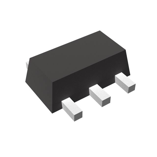
The packages for these ICs are the SOT-89-5 for space saving and the HSOP-6J for higher power applications.
FEATURES
•
•
•
•
•
•
•
•
•
•
•
•
•
Input Voltage Range (Maximum Rating) ............... 4V to 36V (50V)
Supply Current ...................................................... Typ. 9µA
Standby Current .................................................... Typ. 0.1µA
Temperature-Drift Coefficient of Output Voltage ... Typ. ±100ppm/°C
Output Current ...................................................... Min. 50mA (VIN=VOUT+3.0V)
Line Regulation ..................................................... Typ. 0.05%/V
Output Voltage Accuracy....................................... ±2%
Packages .............................................................. SOT-89-5, HSOP-6J
Output Voltage Range........................................... 2.0V to 12.0V (0.1V step)
Built-in Peak Current Limit Circuit
Built-in Short Current Limit Circuit ....................... Typ. 50mA
Built-in Thermal Shutdown Circuit
Operating Temperature ......................................... −40°C to 105°C
APPLICATIONS
• Power source for car accessories such as car audio equipment, car navigation system, and ETC system.
• Power source for ECUs such as EV inverter and battery charge control unit.
1
�R1515x
NO.EC-153-150701
BLOCK DIAGRAM
R1515xxxxB
VDD
Thermal Shutdown
Circuit
Internal
VR
VOUT
Vref
Short
Current Limit
Protection
GND
CE
SELECTION GUIDE
The output voltage and the package for the ICs can be selected at the user’s request.
Product Name
Package
Quantity per Reel
Pb Free
Halogen Free
R1515HxxxB-T1-#E
SOT-89-5
1,000 pcs
Yes
Yes
R1515SxxxB-E2-#E
HSOP-6J
1,000 pcs
Yes
Yes
xxx : The output voltage can be designated in the range of 2.0V (020) to 12.0V (120) in 0.1V step.
# : Specify Automotive Class Code
Operating
Temperature Range
A
-40°C to 105°C
J
-40°C to 105°C
2
Guaranteed Specs
Temperature Range
25°C
25°C
Screening
High Temperature
High and Low Temperature
�R1515x
NO.EC-153-150701
PIN DESCRIPTIONS
• SOT-89-5
5
1
•
• HSOP-6J
4
2
3
6
5
4
1
2
3
SOT-89-5
Pin No.
Symbol
Description
1
VOUT
Output Pin
2
GND∗
Ground Pin
3
CE
4
GND∗
5
VDD
Chip Enable Pin ("H" Active)
Ground Pin
Input Pin
∗) The GND pin must be wired together when it is mounted on board.
•
HSOP-6J
Pin No.
Symbol
Description
1
VOUT
Output Pin
2
GND∗
Ground Pin
3
CE
Chip Enable Pin ("H" Active)
4
GND
∗
Ground Pin
5
GND∗
Ground Pin
6
VDD
Input Pin
∗) The GND pin must be wired together when it is mounted on board.
3
�R1515x
NO.EC-153-150701
ABSOLUTE MAXIMUM RATINGS
Item
Symbol
Rating
Unit
−0.3~50
V
60
V
VIN
Input Voltage
VIN
Peak Input Voltage
VCE
Input Voltage (CE Pin)
−0.3~VIN+0.3≤50
V
VOUT
Output Voltage
−0.3~VIN+0.3≤50
V
IOUT
Output Current
150
mA
*1
SOT-89-5
PD
Power Dissipation*2
HSOP-6J
Tj
Tstg
Standard Land Pattern
900
High Wattage Land Pattern
1300
Standard Land Pattern
1700
Ultra High Wattage Land Pattern
2700
mW
Junction Temperature
−40 to 125
°C
Storage Temperature Range
−55 to 125
°C
*1
Duration time: 200ms
*2
Refer to PACKAGE INFORMATION for detailed information.
ABSOLUTE MAXIMUM RATINGS
Electronic and mechanical stress momentarily exceeded absolute maximum ratings may cause the permanent damages
and may degrade the life time and safety for both device and system using the device in the field. The functional
operation at or over these absolute maximum ratings is not assured.
RECOMMENDED OPERATING CONDITIONS
Symbol
Item
VIN
Input Voltage
Ta
Operating Temperature Range
Rating
Unit
4 to 36
V
−40 to 105
°C
RECOMMENDED OPERATING CONDITIONS
All of electronic equipment should be designed that the mounted semiconductor devices operate within the recommended
operating conditions. The semiconductor devices cannot operate normally over the recommended operating conditions,
even if when they are used over such conditions by momentary electronic noise or surge. And the semiconductor devices
may receive serious damage when they continue to operate over the recommended operating conditions.
4
�R1515x
NO.EC-153-150701
ELECTRICAL CHARACTERISTICS
The specifications surrounded by
are guaranteed by design engineering at -40°C ≤ Ta ≤ 105 °C.
(Ta=25°C)
R1515xxxxB
Symbol
ISS
Item
Conditions
Min.
Typ.
Max.
Unit
9
20
µA
0.1
1.0
µA
×0.98
×1.02
V
×0.97
×1.03
V
Supply Current
VIN=VOUT+3.0V, IOUT=0mA
Standby Current
VIN=36V, VCE=0V
VOUT
Output Voltage
VIN=VOUT+3.0V,
IOUT=1mA
IOUT
Output Current
VIN=VOUT+3.0V
50
∆VOUT/∆IOUT
Load Regulation
VIN=VOUT+3.0V,
1mA ≤ IOUT ≤ 40mA
Refer to the Product-specific
Electrical Characteristics
∆VOUT/∆VIN
Line Regulation
VOUT+1.5V ≤ VIN ≤ 36V, IOUT=1mA
VDIF
Dropout Voltage
IOUT=20mA
ISC
Short Current Limit
VOUT=0V
Istandby
Ta = 25°C
−40°C ≤ Ta ≤ 105°C
mA
0.05
0.20
%/V
Refer to the Product-specific
Electrical Characteristics
50
mA
VCEH
CE Input Voltage "H"
1.5
VIN
V
VCEL
CE Input Voltage "L"
0
0.3
V
TTSD
TTSR
Thermal Shutdown
Temperature
Thermal Shutdown
Released Temperature
Junction Temperature
150
°C
Junction Temperature
125
°C
All test items listed under Electrical Characteristics are done under the pulse load condition (Tj ≈ Ta = 25°C).
5
�R1515x
NO.EC-153-150701
Product-specific Electrical Characteristics
The specifications surrounded by
are guaranteed by design engineering at -40°C ≤ Ta ≤ 105 °C
(Ta = 25°C)
Product
Name
VOUT [V]
Ta = 25°C
MIN.
TYP.
MAX.
−40°C ≤ Ta ≤ 105°C
MIN.
TYP. MAX.
ΔVOUT/ΔIOUT
[mV]
TYP. MAX.
VDIF [V]
TYP.
Ta = 25°C −40°C ≤ Ta ≤ 105°C
MAX.
MAX.
R1515x020B 1.960 2.000 2.040 1.940 2.000 2.060
2.00
2.00
R1515x021B 2.058 2.100 2.142 2.037 2.100 2.163
1.90
1.90
R1515x022B 2.156 2.200 2.244 2.134 2.200 2.266
1.80
1.80
R1515x023B 2.254 2.300 2.346 2.231 2.300 2.369
1.70
1.70
R1515x024B 2.352 2.400 2.448 2.328 2.400 2.472
1.60
1.60
R1515x025B 2.450 2.500 2.550 2.425 2.500 2.575
1.50
1.50
R1515x026B 2.548 2.600 2.652 2.522 2.600 2.678
1.40
1.40
R1515x027B 2.646 2.700 2.754 2.619 2.700 2.781
1.30
1.30
1.20
1.20
R1515x029B 2.842 2.900 2.958 2.813 2.900 2.987
1.10
1.10
R1515x030B 2.940 3.000 3.060 2.910 3.000 3.090
1.00
1.00
R1515x031B 3.038 3.100 3.162 3.007 3.100 3.193
0.90
0.90
R1515x032B 3.136 3.200 3.264 3.104 3.200 3.296
0.80
0.80
0.70
0.70
0.60
0.70
R1515x035B 3.430 3.500 3.570 3.395 3.500 3.605
0.50
0.60
R1515x036B 3.528 3.600 3.672 3.492 3.600 3.708
0.40
0.60
0.35
0.60
0.60
0.25
0.40
0.50
R1515x028B 2.744 2.800 2.856 2.716 2.800 2.884
−
R1515x033B 3.234 3.300 3.366 3.201 3.300 3.399
R1515x034B 3.332 3.400 3.468 3.298 3.400 3.502
10
25
R1515x037B 3.626 3.700 3.774 3.589 3.700 3.811
R1515x038B 3.724 3.800 3.876 3.686 3.800 3.914
R1515x039B 3.822 3.900 3.978 3.783 3.900 4.017
R1515x040B 3.920 4.000 4.080 3.880 4.000 4.120
R1515x041B 4.018 4.100 4.182 3.977 4.100 4.223
R1515x042B 4.116 4.200 4.284 4.074 4.200 4.326
R1515x043B 4.214 4.300 4.386 4.171 4.300 4.429
R1515x044B 4.312 4.400 4.488 4.268 4.400 4.532
R1515x045B 4.410 4.500 4.590 4.365 4.500 4.635
R1515x046B 4.508 4.600 4.692 4.462 4.600 4.738
R1515x047B 4.606 4.700 4.794 4.559 4.700 4.841
R1515x048B 4.704 4.800 4.896 4.656 4.800 4.944
R1515x049B 4.802 4.900 4.998 4.753 4.900 5.047
6
�R1515x
NO.EC-153-150701
(Ta=25°C)
Product
Name
VOUT [V]
Ta = 25°C
MIN.
TYP.
MAX.
−40°C ≤ Ta ≤ 105°C
MIN.
TYP. MAX.
ΔVOUT/ΔIOUT
[mV]
TYP. MAX.
VDIF [V]
TYP.
Ta = 25°C −40°C ≤ Ta ≤ 105°C
MAX.
MAX.
0.35
0.40
R1515x050B 4.900 5.000 5.100 4.850 5.000 5.150
R1515x051B 4.998 5.100 5.202 4.947 5.100 5.253
R1515x052B 5.096 5.200 5.304 5.044 5.200 5.356
R1515x053B 5.194 5.300 5.406 5.141 5.300 5.459
R1515x054B 5.292 5.400 5.508 5.238 5.400 5.562
R1515x055B 5.390 5.500 5.610 5.335 5.500 5.665
R1515x056B 5.488 5.600 5.712 5.432 5.600 5.768
R1515x057B 5.586 5.700 5.814 5.529 5.700 5.871
R1515x058B 5.684 5.800 5.916 5.626 5.800 5.974
R1515x059B 5.782 5.900 6.018 5.723 5.900 6.077
R1515x060B 5.880 6.000 6.120 5.820 6.000 6.180
R1515x061B 5.978 6.100 6.222 5.917 6.100 6.283
R1515x062B 6.076 6.200 6.324 6.014 6.200 6.386
R1515x063B 6.174 6.300 6.426 6.111 6.300 6.489
R1515x064B 6.272 6.400 6.528 6.208 6.400 6.592
R1515x065B 6.370 6.500 6.630 6.305 6.500 6.695
R1515x066B 6.468 6.600 6.732 6.402 6.600 6.798
R1515x067B 6.566 6.700 6.834 6.499 6.700 6.901
R1515x068B 6.664 6.800 6.936 6.596 6.800 7.004
R1515x069B 6.762 6.900 7.038 6.693 6.900 7.107
R1515x070B 6.860 7.000 7.140 6.790 7.000 7.210
20
35
0.20
R1515x071B 6.958 7.100 7.242 6.887 7.100 7.313
R1515x072B 7.056 7.200 7.344 6.984 7.200 7.416
R1515x073B 7.154 7.300 7.446 7.081 7.300 7.519
R1515x074B 7.252 7.400 7.548 7.178 7.400 7.622
R1515x075B 7.350 7.500 7.650 7.275 7.500 7.725
R1515x076B 7.448 7.600 7.752 7.372 7.600 7.828
R1515x077B 7.546 7.700 7.854 7.469 7.700 7.931
R1515x078B 7.644 7.800 7.956 7.566 7.800 8.034
R1515x079B 7.742 7.900 8.058 7.663 7.900 8.137
R1515x080B 7.840 8.000 8.160 7.760 8.000 8.240
R1515x081B 7.938 8.100 8.262 7.857 8.100 8.343
R1515x082B 8.036 8.200 8.364 7.954 8.200 8.446
R1515x083B 8.134 8.300 8.466 8.051 8.300 8.549
R1515x084B 8.232 8.400 8.568 8.148 8.400 8.652
R1515x085B 8.330 8.500 8.670 8.245 8.500 8.755
R1515x086B 8.428 8.600 8.772 8.342 8.600 8.858
R1515x087B 8.526 8.700 8.874 8.439 8.700 8.961
R1515x088B 8.624 8.800 8.976 8.536 8.800 9.064
R1515x089B 8.722 8.900 9.078 8.633 8.900 9.167
7
�R1515x
NO.EC-153-150701
(Ta = 25°C)
Product
Name
VOUT [V]
Ta = 25°C
−40°C ≤ Ta ≤ 105°C
MAX.
MIN.
TYP.
MAX.
R1515x090B 8.820 9.000 9.180
8.730
9.000
9.270
R1515x091B 8.918 9.100 9.282
8.827
9.100
9.373
R1515x092B 9.016 9.200 9.384
8.924
9.200
9.476
R1515x093B 9.114 9.300 9.486
9.021
9.300
9.579
R1515x094B 9.212 9.400 9.588
9.118
9.400
9.682
R1515x095B 9.310 9.500 9.690
9.215
9.500
9.785
R1515x096B 9.408 9.600 9.792
9.312
9.600
9.888
R1515x097B 9.506 9.700 9.894
9.409
9.700
9.991
R1515x098B 9.604 9.800 9.996
9.506
9.800 10.094
R1515x099B 9.702 9.900 10.098 9.603
9.900 10.197
MIN.
TYP.
ΔVOUT/ΔIOUT
[mV]
TYP. MAX.
VDIF [V]
TYP.
Ta = 25°C −40°C ≤ Ta ≤ 105°C
MAX.
MAX.
0.35
0.40
R1515x100B 9.800 10.000 10.200 9.700 10.000 10.300
R1515x101B 9.898 10.100 10.302 9.797 10.100 10.403
R1515x102B 9.996 10.200 10.404 9.894 10.200 10.506
R1515x103B 10.094 10.300 10.506 9.991 10.300 10.609
R1515x104B 10.192 10.400 10.608 10.088 10.400 10.712
R1515x105B 10.290 10.500 10.710 10.185 10.500 10.815
R1515x106B 10.388 10.600 10.812 10.282 10.600 10.918
R1515x107B 10.486 10.700 10.914 10.379 10.700 11.021
R1515x108B 10.584 10.800 11.016 10.476 10.800 11.124
R1515x109B 10.682 10.900 11.118 10.573 10.900 11.227
R1515x110B 10.780 11.000 11.220 10.670 11.000 11.330
R1515x111B 10.878 11.100 11.322 10.767 11.100 11.433
R1515x112B 10.976 11.200 11.424 10.864 11.200 11.536
R1515x113B 11.074 11.300 11.526 10.961 11.300 11.639
R1515x114B 11.172 11.400 11.628 11.058 11.400 11.742
R1515x115B 11.270 11.500 11.730 11.155 11.500 11.845
R1515x116B 11.368 11.600 11.832 11.252 11.600 11.948
R1515x117B 11.466 11.700 11.934 11.349 11.700 12.051
R1515x118B 11.564 11.800 12.036 11.446 11.800 12.154
R1515x119B 11.662 11.900 12.138 11.543 11.900 12.257
R1515x120B 11.760 12.000 12.240 11.640 12.000 12.360
8
20
35
0.20
�R1515x
NO.EC-153-150701
TYPICAL APPLICATION
VDD
C1
VOUT
VOUT
R1515x
Series
CE
C2
GND
External Parts Example:
C1
0.1µF (Ceramic)
C2
0.1µF (Ceramic)
TECHNICAL NOTES
When using these ICs, consider the following points:
Phase Compensation
Phase Compensation of the R1515x Series has been made internally for stable operation even though the load
current would vary. Therefore, without the capacitors, C1 and C2, the output voltage is regulated, however, for
more stable operation, use capacitors as C1 and C2. Especially, if the input line is long and impedance is high,
C1 is necessary. Moreover, if you use rather large C2, transient response will be improved. Recommended value
is in the range from 0.1µF to 10µF. Wiring should be made as short as possible.
Connect the capacitor, C1 between VDD pin and GND pin and C2 between VOUT and GND as close as possible.
GND wiring of mounting on board
No.2 pin and No.4 pin of SOT-89-5 package must be wired to the GND plane. No.2 pin, No.4 pin and No.5 pin
of HSOP-6J package must be wired to the GND plane when it is mounted on board.
Thermal Shutdown
Thermal shutdown function is included in the R1515x Series, if the junction temperature is equal or more than
+150°C (Typ.), the operation of regulator would stop. After that, when the junction temperature is equal or less
than +125°C (Typ.), the operation of regulator would restart. Unless the cause of rising temperature would remove,
the regulator repeats on and off, and output waveform would be like consecutive pulses.
Chip Enable Circuit
Do not make voltage level of chip enable pin keep floating level, or in between VCEH and VCEL. Otherwise, the
output voltage would be unstable or indefinite, or unexpected current would flow internally.
9
�R1515x
NO.EC-153-150701
TYPICAL APPLICATION FOR IC CHIP BREAKDOWN PREVENTION
VDD
C1
R1515x
Series
CE
VOUT
VOUT
C2
D1
GND
When a sudden surge of electrical current travels along the VOUT pin and GND due to a short-circuit, electrical
resonance of a circuit involving an output capacitor (C2) and a short circuit inductor generates a negative voltage
and may damage the device or the load devices. Connecting a schottky diode (D1) between the VOUT pin and
GND has the effect of preventing damage to them.
10
�R1515x
NO.EC-153-150701
PACKAGE INFORMATION
POWER DISSIPATION (SOT-89-5)
Power Dissipation (PD) depends on conditions of mounting on board. This specification is based on the
measurement at the condition below:
Measurement Conditions (SOT-89-5)
High Wattage Land Pattern
Environment
Standard Land Pattern
Mounting on board (Wind velocity = 0 m/s) Mounting on board (Wind velocity = 0 m/s)
Board Material
Glass cloth epoxy plastic (Double sided)
Glass cloth epoxy plastic (Double sided)
Board Dimensions
30 mm x 30 mm x 1.6 mm
50 mm x 50 mm x 1.6 mm
Copper Ratio
Top side: Approx. 20% ,
Back side: Approx. 100%
Top side: Approx. 10% ,
Back side: Approx. 100%
Through-hole
φ0.85 mm x 10 pcs
(Ta = 25°C, Tjmax = 125°C)
Standard Land Pattern
Free Air
Power Dissipation
1300 mW
900 mW
500 mW
Thermal Resistance
77°C/W
111°C/W
200°C/W
1500
1400
1300
1200
1100
1000
900
800
700
600
500
400
300
200
100
0
On Board
(High Wattage Land Pattern)
On Board
(Standard Land Pattern)
30
7.5
50
15
7.5
50
15
Free Air
30
Power Dissipation PD (mW)
Measurement Result (SOT-89-5)
High Wattage Land Pattern
0
25
50
75
105
100
125
High Wattage
150
Ambient Temperature (°C)
Power Dissipation vs. Ambience Temperature
(SOT-89-5)
Standard
IC Mount Area (Unit: mm)
Measurement Board Pattern
(SOT-89-5)
11
�R1515x
NO.EC-153-150701
PACKAGE DIMENSIONS (SOT-89-5)
4.5±0.1
1.5±0.1
0.4±0.3
2
5
4.35±0.1
φ1.0
1
4
4
2.5±0.1
1.00±0.2
5
0.4±0.1
0.1 S
3
3
2
1
0.4±0.1
Bottom View
S
0.42±0.1
0.42±0.1
0.47±0.1
1.5±0.1
1.5±0.1
Unit: mm
MARK SPECIFICATION (SOT-89-5)
: Product Code … Refer to R1515H MARK SPECIFICATION TABLE
: Lot Number … Alphanumeric Serial Number
12
0.3±0.2
0.42±0.1
0.3±0.2
1.6±0.2
�R1515x
NO.EC-153-150701
R1515H MARK SPECIFICATION TABLE (SOT-89-5)
Product
Name
R1515H020B
R1515H021B
R1515H022B
R1515H023B
R1515H024B
R1515H025B
R1515H026B
R1515H027B
R1515H028B
R1515H029B
R1515H030B
R1515H031B
R1515H032B
R1515H033B
R1515H034B
R1515H035B
R1515H036B
R1515H037B
R1515H038B
R1515H039B
R1515H040B
R1515H041B
R1515H042B
R1515H043B
R1515H044B
R1515H045B
R1515H046B
R1515H047B
R1515H048B
R1515H049B
R1515H050B
R1515H051B
R1515H052B
R1515H053B
R1515H054B
R1515H055B
R1515H056B
R1515H057B
R1515H058B
R1515H059B
VSET
N020
N021
N022
N023
N024
N025
N026
N027
N028
N029
N030
N031
N032
N033
N034
N035
N036
N037
N038
N039
N040
N041
N042
N043
N044
N045
N046
N047
N048
N049
N050
N051
N052
N053
N054
N055
N056
N057
N058
N059
2.0 V
2.1 V
2.2 V
2.3 V
2.4 V
2.5 V
2.6 V
2.7 V
2.8 V
2.9 V
3.0 V
3.1 V
3.2 V
3.3 V
3.4 V
3.5 V
3.6 V
3.7 V
3.8 V
3.9 V
4.0 V
4.1 V
4.2 V
4.3 V
4.4 V
4.5 V
4.6 V
4.7 V
4.8 V
4.9 V
5.0 V
5.1 V
5.2 V
5.3 V
5.4 V
5.5 V
5.6 V
5.7 V
5.8 V
5.9 V
Product
Name
R1515H060B
R1515H061B
R1515H062B
R1515H063B
R1515H064B
R1515H065B
R1515H066B
R1515H067B
R1515H068B
R1515H069B
R1515H070B
R1515H071B
R1515H072B
R1515H073B
R1515H074B
R1515H075B
R1515H076B
R1515H077B
R1515H078B
R1515H079B
R1515H080B
R1515H081B
R1515H082B
R1515H083B
R1515H084B
R1515H085B
R1515H086B
R1515H087B
R1515H088B
R1515H089B
R1515H090B
R1515H091B
R1515H092B
R1515H093B
R1515H094B
R1515H095B
R1515H096B
R1515H097B
R1515H098B
R1515H099B
VSET
N060
N061
N062
N063
N064
N065
N066
N067
N068
N069
N070
N071
N072
N073
N074
N075
N076
N077
N078
N079
N080
N081
N082
N083
N084
N085
N086
N087
N088
N089
N090
N091
N092
N093
N094
N095
N096
N097
N098
N099
6.0 V
6.1 V
6.2 V
6.3 V
6.4 V
6.5 V
6.6 V
6.7 V
6.8 V
6.9 V
7.0 V
7.1 V
7.2 V
7.3 V
7.4 V
7.5 V
7.6 V
7.7 V
7.8 V
7.9 V
8.0 V
8.1 V
8.2 V
8.3 V
8.4 V
8.5 V
8.6 V
8.7 V
8.8 V
8.9 V
9.0 V
9.1 V
9.2 V
9.3 V
9.4 V
9.5 V
9.6 V
9.7 V
9.8 V
9.9 V
Product
Name
R1515H100B
R1515H101B
R1515H102B
R1515H103B
R1515H104B
R1515H105B
R1515H106B
R1515H107B
R1515H108B
R1515H109B
R1515H110B
R1515H111B
R1515H112B
R1515H113B
R1515H114B
R1515H115B
R1515H116B
R1515H117B
R1515H118B
R1515H119B
R1515H120B
VSET
N100
N101
N102
N103
N104
N105
N106
N107
N108
N109
N110
N111
N112
N113
N114
N115
N116
N117
N118
N119
N120
10.0 V
10.1 V
10.2 V
10.3 V
10.4 V
10.5 V
10.6 V
10.7 V
10.8 V
10.9 V
11.0 V
11.1 V
11.2 V
11.3 V
11.4 V
11.5 V
11.6 V
11.7 V
11.8 V
11.9 V
12.0 V
13
�R1515x
NO.EC-153-150701
POWER DISSIPATION (HSOP-6J)
Power Dissipation (PD) depends on conditions of mounting on board. This specification is based on the
measurement at the condition below:
Measurement Conditions
Ultra High Wattage Land Pattern
Environment
Standard Land Pattern
Mounting on Board (Wind velocity = 0 m/s) Mounting on Board (Wind velocity = 0 m/s)
Board Material
Glass cloth epoxy plastic (4 Layers)
Glass cloth epoxy plastic (2 Layers)
Board Dimensions
76.2 mm×114.3 mm×0.8 mm
50 mm × 50 mm × 1.6 mm
Copper Ratio
96%
Through-hole
Measurement Result
φ0.3 mm × 28 pcs
50%
φ0.5 mm × 24 pcs
(Ta = 25°C, Tjmax = 125°C)
Ultra High Wattage Land
Pattern
Standard Land Pattern
Free Air
Power Dissipation
2700 mW
1700 mW
540 mW
Thermal Resistance
37°C/W
59°C/W
185°C/W
Power Dissipation PD (mW)
3500
3000 2700
On Board
2750
(Ultra High Wattage Land Pattern)
2500
2250
2000 1700
1750
1500
1250
1000
750
On Board
500 (Standard Land Pattern)
250
0
76.2
0
25
50
75
100 125 150
105
Ambient Temperature (°C)
50
50
20
40
20
50
114.3
40
Power Dissipation
Standard
Ultra High Wattage Land Pattern
IC mount area (Unit: mm)
14
Measurement Board Pattern
IC Mount Area (Unit: mm)
�R1515x
NO.EC-153-150701
PACKAGE DIMENSIONS (HSOP-6J)
5.02±0.3
4
0.60±0.2
3.9±0.2
5
6.0±0.3
6
1
2
3
3.81
+0.10
0.2-0.05
1.67±0.1
0.4±0.1
0.10
0.12 M
0.15±0.1
1.5±0.1
0.605TYP.
Unit: mm
MARK SPECIFICATION (HSOP-6J)
: Product Code … Refer to R1515S MARK SPECIFICATION TABLE
: Lot Number … Alphanumeric Serial Number
R
15
�R1515x
NO.EC-153-150701
R1515S MARK SPECIFICATION TABLE (HSOP-6J)
Product
Name
R1515S020B
VSET
VSET
2.0 V
Product
Name
R1515S060B
VSET
6.0 V
Product
Name
R1515S100B
F020
F060
F100
10.0 V
R1515S021B
F021
2.1 V
R1515S061B
F061
6.1 V
R1515S101B
F101
10.1 V
R1515S022B
F022
2.2 V
R1515S023B
F023
2.3 V
R1515S062B
F062
6.2 V
R1515S102B
F102
10.2 V
R1515S063B
F063
6.3 V
R1515S103B
F103
10.3 V
R1515S024B
F024
2.4 V
R1515S064B
F064
6.4 V
R1515S104B
F104
10.4 V
R1515S025B
F025
R1515S026B
F026
2.5 V
R1515S065B
F065
6.5 V
R1515S105B
F105
10.5 V
2.6 V
R1515S066B
F066
6.6 V
R1515S106B
F106
R1515S027B
F027
10.6 V
2.7 V
R1515S067B
F067
6.7 V
R1515S107B
F107
10.7 V
R1515S028B
F028
R1515S029B
F029
2.8 V
R1515S068B
F068
6.8 V
R1515S108B
F108
10.8 V
2.9 V
R1515S069B
F069
6.9 V
R1515S109B
F109
R1515S030B
F030
10.9 V
3.0 V
R1515S070B
F070
7.0 V
R1515S110B
F110
11.0 V
R1515S031B
F031
R1515S032B
F032
3.1 V
R1515S071B
F071
7.1 V
R1515S111B
F111
11.1 V
3.2 V
R1515S072B
F072
7.2 V
R1515S112B
F112
R1515S033B
F033
11.2 V
3.3 V
R1515S073B
F073
7.3 V
R1515S113B
F113
11.3 V
R1515S034B
F034
3.4 V
R1515S074B
F074
7.4 V
R1515S114B
F114
11.4 V
R1515S035B
F035
3.5 V
R1515S075B
F075
7.5 V
R1515S115B
F115
11.5 V
R1515S036B
F036
3.6 V
R1515S076B
F076
7.6 V
R1515S116B
F116
11.6 V
R1515S037B
F037
3.7 V
R1515S077B
F077
7.7 V
R1515S117B
F117
11.7 V
R1515S038B
F038
3.8 V
R1515S078B
F078
7.8 V
R1515S118B
F118
11.8 V
R1515S039B
F039
3.9 V
R1515S079B
F079
7.9 V
R1515S119B
F119
11.9 V
R1515S040B
F040
4.0 V
R1515S080B
F080
8.0 V
R1515S120B
F120
12.0 V
R1515S041B
F041
4.1 V
R1515S081B
F081
8.1 V
R1515S042B
F042
4.2 V
R1515S082B
F082
8.2 V
R1515S043B
F043
4.3 V
R1515S083B
F083
8.3 V
R1515S044B
F044
4.4 V
R1515S084B
F084
8.4 V
R1515S045B
F045
4.5 V
R1515S085B
F085
8.5 V
R1515S046B
F046
4.6 V
R1515S086B
F086
8.6 V
R1515S047B
F047
4.7 V
R1515S087B
F087
8.7 V
R1515S048B
F048
4.8 V
R1515S088B
F088
8.8 V
R1515S049B
F049
4.9 V
R1515S089B
F089
8.9 V
R1515S050B
F050
5.0 V
R1515S090B
F090
9.0 V
R1515S051B
F051
5.1 V
R1515S091B
F091
9.1 V
R1515S052B
F052
5.2 V
R1515S092B
F092
9.2 V
R1515S053B
F053
5.3 V
R1515S093B
F093
9.3 V
R1515S054B
F054
5.4 V
R1515S094B
F094
9.4 V
R1515S055B
F055
5.5 V
R1515S095B
F095
9.5 V
R1515S056B
F056
5.6 V
R1515S096B
F096
9.6 V
R1515S057B
F057
5.7 V
R1515S097B
F097
9.7 V
R1515S058B
F058
5.8 V
R1515S098B
F098
9.8 V
R1515S059B
F059
5.9 V
R1515S099B
F099
9.9 V
16
�R1515x
NO.EC-153-150701
TYPICAL CHARACTERISTICS
Note: Typical Characteristics are intended to be used as reference data; they are not guaranteed.
1) Output Voltage vs. Output Current (Ta=25°C)
R1515x020B
R1515x030B
R1515x050B
R1515x090B
2) Output Voltage vs. Input Voltage (Ta=25°C)
R1515x020B
R1515x030B
17
�R1515x
NO.EC-153-150701
R1515x050B
R1515x090B
3) Dropout Voltage vs. Output Current
R1515x050B
R1515x090B
4) Output Voltage vs. Temperature
R1515x020B
18
R1515x030B
�R1515x
NO.EC-153-150701
R1515x050B
R1515x090B
5) Supply Current vs. Input Voltage (Ta=25°C)
R1515x020B
R1515x030B
R1515x050B
R1515x090B
19
�R1515x
NO.EC-153-150701
6) Supply Current vs. Temperature
R1515x020B
R1515x030B
R1515x050B
R1515x090B
7) Input Transient Response (IOUT=1mA, tr=tf=50µs, C2=Ceramic 0.1µF, Ta=25°C)
R1515x020B
20
R1515x030B
�R1515x
NO.EC-153-150701
R1515x050B
R1515x090B
8) Load Transient Response (C2=Ceramic 0.1µF, Ta=25°C)
21
�1. The products and the product specifications described in this document are subject to change or discontinuation of
production without notice for reasons such as improvement. Therefore, before deciding to use the products, please
refer to Ricoh sales representatives for the latest information thereon.
2. The materials in this document may not be copied or otherwise reproduced in whole or in part without prior written
consent of Ricoh.
3. Please be sure to take any necessary formalities under relevant laws or regulations before exporting or otherwise
taking out of your country the products or the technical information described herein.
4. The technical information described in this document shows typical characteristics of and example application circuits
for the products. The release of such information is not to be construed as a warranty of or a grant of license under
Ricoh's or any third party's intellectual property rights or any other rights.
5. The products in this document are designed for automotive applications. However, when using the products for
automotive applications, please make sure to contact Ricoh sales representative in advance due to confirming the
quality level.
6. We are making our continuous effort to improve the quality and reliability of our products, but semiconductor products
are likely to fail with certain probability. In order to prevent any injury to persons or damages to property resulting from
such failure, customers should be careful enough to incorporate safety measures in their design, such as redundancy
feature, fire containment feature and fail-safe feature. We do not assume any liability or responsibility for any loss or
damage arising from misuse or inappropriate use of the products.
7. Anti-radiation design is not implemented in the products described in this document.
8. The X-ray exposure can influence functions and characteristics of the products. Confirm the product functions and
characteristics in the evaluation stage.
9. WLCSP products should be used in light shielded environments. The light exposure can influence functions and
characteristics of the products under operation or storage.
10. There can be variation in the marking when different AOI (Automated Optical Inspection) equipment is used.
In the case of recognizing the marking characteristic with AOI, please contact Ricoh sales or our distributor before
attempting to use AOI.
11. Please contact Ricoh sales representatives should you have any questions or comments concerning the products or
the technical information.
Halogen Free
Ricoh is committed to reducing the environmental loading materials in electrical devices
with a view to contributing to the protection of human health and the environment.
Ricoh has been providing RoHS compliant products since April 1, 2006 and Halogen-free products since
April 1, 2012.
https://www.e-devices.ricoh.co.jp/en/
Sales & Support Offices
Ricoh Electronic Devices Co., Ltd.
Shin-Yokohama Office (International Sales)
2-3, Shin-Yokohama 3-chome, Kohoku-ku, Yokohama-shi, Kanagawa, 222-8530, Japan
Phone: +81-50-3814-7687 Fax: +81-45-474-0074
Ricoh Americas Holdings, Inc.
675 Campbell Technology Parkway, Suite 200 Campbell, CA 95008, U.S.A.
Phone: +1-408-610-3105
Ricoh Europe (Netherlands) B.V.
Semiconductor Support Centre
Prof. W.H. Keesomlaan 1, 1183 DJ Amstelveen, The Netherlands
Phone: +31-20-5474-309
Ricoh International B.V. - German Branch
Semiconductor Sales and Support Centre
Oberrather Strasse 6, 40472 Düsseldorf, Germany
Phone: +49-211-6546-0
Ricoh Electronic Devices Korea Co., Ltd.
3F, Haesung Bldg, 504, Teheran-ro, Gangnam-gu, Seoul, 135-725, Korea
Phone: +82-2-2135-5700 Fax: +82-2-2051-5713
Ricoh Electronic Devices Shanghai Co., Ltd.
Room 403, No.2 Building, No.690 Bibo Road, Pu Dong New District, Shanghai 201203,
People's Republic of China
Phone: +86-21-5027-3200 Fax: +86-21-5027-3299
Ricoh Electronic Devices Shanghai Co., Ltd.
Shenzhen Branch
1205, Block D(Jinlong Building), Kingkey 100, Hongbao Road, Luohu District,
Shenzhen, China
Phone: +86-755-8348-7600 Ext 225
Ricoh Electronic Devices Co., Ltd.
Taipei office
Room 109, 10F-1, No.51, Hengyang Rd., Taipei City, Taiwan (R.O.C.)
Phone: +886-2-2313-1621/1622 Fax: +886-2-2313-1623
�


 工商网监
湘ICP备2023018690号
工商网监
湘ICP备2023018690号