R1515x SERIES
50mA VOLTAGE REGULATOR (Wide Input Voltage Range)
NO.EA-153-111026
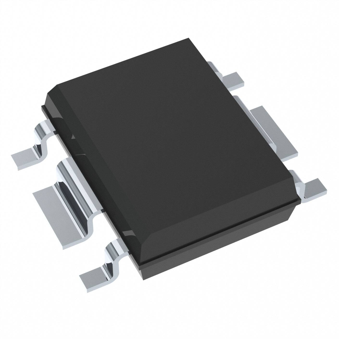
OUTLINE
The R1515x series are CMOS-based positive voltage regulator (VR) ICs featuring 50mA output current. The
R1515xxxxB has features of high input voltage and ultra-low supply current. A peak current limit circuit, a short
current limit circuit, and a thermal shutdown circuit are built in the R1515x series.
The operating temperature is −40°C to 105°C and the maximum input voltage is 36V, the R1515x series are
very suitable for power source of car accessories.
The regulator output voltage is fixed in the R1515xxxxB and can be selected with a step of 0.1V in the range of
2.0V to 12.0V. Output voltage accuracy is ±2%.
The packages for these ICs are the SOT-89-5 for space saving and the HSOP-6J for higher power
applications.
FEATURES
•
•
•
•
•
•
•
•
•
•
•
•
•
Input Voltage ......................................................... Max. 36V
Supply Current ......................................................Typ. 9μA
Standby Current ....................................................Typ. 0.1μA
Temperature-Drift Coefficient of Output Voltage ...Typ. ±100ppm/°C
Output Current ......................................................Min. 50mA (VIN=VOUT+3.0V; R1515x050B)
Line Regulation .....................................................Typ. 0.05%/V
Output Voltage Accuracy.......................................±2%
Output Voltage Range...........................................2.0V to 12.0V (0.1V steps)
(For other voltages, please refer to MARK INFORMATIONS.)
Packages ..............................................................SOT-89-5, HSOP-6J
Built-in Peak Current Limit Circuit
Built-in Short Current Limit Circuit
Built-in Thermal Shutdown Circuit
Operating Temperature ......................................... −40°C to 105°C
APPLICATIONS
•
•
•
•
•
Power source for home appliances such as refrigerators, rice cookers, electric water warmers, etc.
Power source for car audio equipment, car navigation system, ETC system, etc.
Power source for notebook PCs, digital TVs, cordless phones, and private LAN system, etc.
Power source for office equipment machines such as copiers, printers, facsimiles, scanners, projectors, etc.
Power source for the backup circuit for keyless entry system, etc.
1
�R1515x
BLOCK DIAGRAMS
R1515xxxxB
Thermal Shutdown
Circuit
VDD
VOUT
Internal
VR
Vref
Short
Current Limit
Protection
CE
GND
SELECTION GUIDE
The output voltage, package for the ICs can be selected at the user’s request.
Product Name
Package
Quantity per Reel
Pb Free
Halogen Free
R1515HxxxB-T1-FE
SOT-89-5
1,000 pcs
Yes
Yes
R1515SxxxB-E2-FE
HSOP-6J
1,000 pcs
Yes
Yes
xxx : The output voltage can be designated in the range of 2.0V(020) to 12.0V(120) in 0.1V steps.
(For other voltages, please refer to MARK INFORMATIONS.)
2
�R1515x
PIN CONFIGURATIONS
• SOT-89-5
5
1
2
• HSOP-6J
4
6
5
4
3
1
2
3
PIN DESCRIPTIONS
•
SOT-89-5
Pin No.
Symbol
1
VOUT
2
GND
3
CE
4
GND
5
VDD
∗
Description
Output Pin
Ground Pin
Chip Enable Pin ("H" Active)
∗
Ground Pin
Input Pin
∗) The GND pin must be wired together when it is mounted on board.
•
HSOP-6J
Pin No.
Symbol
1
VOUT
2
GND
3
CE
4
GND
5
GND
6
VDD
∗
Description
Output Pin
Ground Pin
Chip Enable Pin ("H" Active)
∗
∗
Ground Pin
Ground Pin
Input Pin
∗) The GND pin must be wired together when it is mounted on board.
3
�R1515x
ABSOLUTE MAXIMUM RATINGS
Symbol
VIN
Item
Input Voltage
∗1
Rating
Unit
−0.3 to 50
V
60
V
VIN
Peak Input Voltage
VCE
Input Voltage (CE Pin)
−0.3 to VIN+0.3 ≤ 50
V
VOUT
Output Voltage
−0.3 to VIN+0.3 ≤ 50
V
IOUT
Output Current
150
mA
∗2
Power Dissipation (SOT-89-5)
PD
∗2
900
mW
Power Dissipation (HSOP-6J)
1700
Topt
Operating Temperature Range
−40 to 105
°C
Tstg
Storage Temperature Range
−55 to 125
°C
∗1) Duration time=200ms
∗2) For Power Dissipation, please refer to PACKAGE INFORMATION.
ABSOLUTE MAXIMUM RATINGS
Electronic and mechanical stress momentarily exceeded absolute maximum ratings may cause the
permanent damages and may degrade the life time and safety for both device and system using the device
in the field.
The functional operation at or over these absolute maximum ratings is not assured.
RECOMMENDED OPERATING CONDITIONS (ELECTRICAL CHARACTERISTICS)
All of electronic equipment should be designed that the mounted semiconductor devices operate within the
recommended operating conditions. The semiconductor devices cannot operate normally over the
recommended operating conditions, even if when they are used over such conditions by momentary
electronic noise or surge. And the semiconductor devices may receive serious damage when they continue
to operate over the recommended operating conditions.
4
�R1515x
ELECTRICAL CHARACTERISTICS
•
R1515xxxxB
Symbol
Topt=25°C
Item
Conditions
VIN
Input Voltage
ISS
Supply Current
VIN=VOUT+3.0V, IOUT=0mA
Standby Current
VIN=36V, VCE=0V
VOUT
Output Voltage
VIN=VOUT+3.0V, IOUT=1mA
IOUT
Output Current
VIN=VOUT+3.0V
ΔVOUT/ΔIOUT
Load Regulation
VIN=VOUT+3.0V,
1mA ≤ IOUT ≤ 40mA
ΔVOUT/ΔVIN
Line Regulation
VOUT+1.5V ≤ VIN ≤ 36V, IOUT=1mA
VDIF
Dropout Voltage
IOUT=20mA
Output Voltage
Temperature Coefficient
VIN=VOUT+3.0V, IOUT=1mA
−40°C ≤ Topt ≤ 105°C
Short Current Limit
VOUT=0V
Istandby
ΔVOUT/ΔTopt
ISC
Min.
Typ.
Max.
Unit
36
V
9
20
μA
0.1
1.0
μA
×1.02
V
4
×0.98
50
mA
Refer to the following table
0.05
0.20
%/V
Refer to the following table
±100
ppm
/°C
50
mA
VCEH
CE Input Voltage "H"
1.5
VIN
V
VCEL
CE Input Voltage "L"
0
0.3
V
TTSD
TTSR
Thermal Shutdown
Temperature
Thermal Shutdown
Released Temperature
Junction Temperature
150
°C
Junction Temperature
125
°C
• Load Regulation by Output Voltage
Output Voltage
VOUT (V)
2.0 ≤ VOUT < 5.0
5.0 ≤ VOUT ≤ 12.0
Topt=25°C
Load Regulation ΔVOUT/ΔIOUT (mV)
Conditions
Typ.
Max.
10
25
VIN=VOUT+3.0V
1mA≤IOUT≤40mA
20
35
• Dropout Voltage by Output Voltage Topt=25°C
Dropout Voltage VDIF (V)
Output Voltage
VOUT (V)
Conditions Typ.
Max.
2.0
VOUT=2.0
1.9
VOUT=2.1
1.8
VOUT=2.2
1.7
VOUT=2.3
1.6
VOUT=2.4
1.5
VOUT=2.5
1.4
VOUT=2.6
1.3
VOUT=2.7
1.2
VOUT=2.8
1.1
VOUT=2.9
IOUT=20mA
1.0
VOUT=3.0
0.9
VOUT=3.1
0.8
VOUT=3.2
0.7
VOUT=3.3
0.6
VOUT=3.4
0.5
VOUT=3.5
0.4
VOUT=3.6
0.35
0.60
3.7 ≤ VOUT < 4.0
0.25
0.40
4.0 ≤ VOUT < 5.0
0.20
0.35
5.0 ≤ VOUT ≤ 12.0
5
�R1515x
TYPICAL APPLICATION
VDD
C1
R1515x
Series
CE
VOUT
VOUT
C2
GND
C1=Ceramic 0.1μF
C2=Ceramic 0.1μF
TECHNICAL NOTES
When using these ICs, consider the following points:
Phase Compensation
Phase Compensation of the R1515x Series has been made internally for stable operation even though the
load current would vary. Therefore, without the capacitors, C1 and C2, the output voltage is regulated, however,
for more stable operation, use capacitors as C1 and C2. Especially, if the input line is long and impedance is high,
C1 is necessary. Moreover, if you use rather large C2, transient response will be improved. Recommended value
is in the range from 0.1μF to 10μF. Wiring should be made as short as possible.
Connect the capacitor, C1 between VDD pin and GND pin and C2 between VOUT and GND as close as possible.
GND wiring of mounting on board
No.2 pin and No.4 pin of SOT-89-5 package must be wired to the GND plane. No.2 pin, No.4 pin and No.5 pin
of HSOP-6J package must be wired to the GND plane when it is mounted on board.
Thermal Shutdown
Thermal shutdown function is included in the R1515x Series, if the junction temperature is equal or more than
+150°C (Typ.), the operation of regulator would stop. After that, when the junction temperature is equal or less
than +125°C (Typ.), the operation of regulator would restart. Unless the cause of rising temperature would
remove, the regulator repeats on and off, and output waveform would be like consecutive pulses.
Chip Enable Circuit
Do not make voltage level of chip enable pin keep floating level, or in between VCEH and VCEL. Otherwise, the
output voltage would be unstable or indefinite, or unexpected current would flow internally.
6
�R1515x
TEST CIRCUITS
VDD
VOUT
R1515x
Series
C1
CE
C2
V
VOUT
IOUT
GND
C1=Ceramic 0.1μF
C2=Ceramic 0.1μF
Basic Test Circuit
VDD
A
ISS
C1
VOUT
VOUT
R1515x
Series
CE
C2
GND
C1=Ceramic 0.1μF
C2=Ceramic 0.1μF
Test Circuit for Supply Current
Pulse
Generator
VDD
P.G.
VOUT
R1515x
Series
CE
C2
IOUT
GND
C2=Ceramic 0.1μF
Test Circuit for Line Transient Response
7
�R1515x
VDD
C1
VOUT
R1515x
Series
CE
VOUT
C2
GND
IOUTa
IOUTb
C1=Ceramic 0.1μF
C2=Ceramic 0.1μF
Test Circuit for Load Transient Response
8
�R1515x
TYPICAL CHARACTERISTICS
1) Output Voltage vs. Output Current (Topt=25°C)
R1515x020B
R1515x030B
3.5
Output Voltage VOUT(V)
Output Voltage VOUT(V)
2.5
2.0
1.5
VIN=3.5V
VIN=4.0V
VIN=4.5V
VIN=5.0V
1.0
0.5
0
3.0
2.5
2.0
VIN=4.5V
VIN=5.0V
VIN=5.5V
VIN=6.0V
1.5
1.0
0.5
0
0
50
100
150
Output Current IOUT(mA)
200
0
R1515x050B
200
R1515x090B
10
Output Voltage VOUT(V)
6
Output Voltage VOUT(V)
50
100
150
Output Current IOUT(mA)
5
4
VIN=6.5V
VIN=7.0V
VIN=7.5V
VIN=8.0V
3
2
1
0
8
6
VIN=10.5V
VIN=11.0V
VIN=11.5V
VIN=12.0V
4
2
0
0
50
100
150
Output Current IOUT(mA)
200
0
50
100
150
Output Current IOUT(mA)
200
2) Output Voltage vs. Input Voltage (Topt=25°C)
R1515x020B
R1515x030B
4.0
Output Voltage VOUT(V)
Output Voltage VOUT(V)
3.0
2.5
2.0
IOUT= 1mA
IOUT=20mA
IOUT=40mA
1.5
1.0
3.5
3.0
IOUT= 1mA
IOUT=20mA
IOUT=40mA
2.5
2.0
0
10
20
30
Input Voltage VIN(V)
40
0
10
20
30
Input Voltage VIN(V)
40
9
�R1515x
R1515x050B
R1515x090B
10.0
Output Voltage VOUT(V)
Output Voltage VOUT(V)
6.0
5.5
5.0
IOUT= 1mA
IOUT=20mA
IOUT=40mA
4.5
4.0
9.5
9.0
IOUT= 1mA
IOUT=20mA
IOUT=40mA
8.5
8.0
0
10
20
30
Input Voltage VIN(V)
40
0
10
20
30
Input Voltage VIN(V)
40
3) Dropout Voltage vs. Output Current
R1515x050B
R1515x090B
2.0
Dropout Voltage VDIF(V)
Dropout Voltage VDIF(V)
2.0
105°C
25°C
-40°C
1.5
1.0
0.5
0
105°C
25°C
-40°C
1.5
1.0
0.5
0
0
10
20
30
40
Output Current IOUT(mA)
50
0
10
20
30
40
Output Current IOUT(mA)
50
4) Output Voltage vs. Temperature
R1515x020B
R1515x030B
VIN=5.0V
VIN=6.0V
2.05
2.00
1.95
1.90
-40 -25
10
3.10
Output Voltage VOUT(V)
Output Voltage VOUT(V)
2.10
0
25
50
75
Temperature Topt(°C)
105
3.05
3.00
2.95
2.90
-40 -25
0
25
50
75
Temperature Topt(°C)
105
�R1515x
R1515x050B
R1515x090B
VIN=8.0V
VIN=12.0V
9.4
Output Voltage VOUT(V)
Output Voltage VOUT(V)
5.2
5.1
5.0
4.9
4.8
-40 -25
0
25
50
75
Temperature Topt(°C)
9.2
9.0
8.8
8.6
-40 -25
105
0
25
50
75
Temperature Topt(°C)
105
5) Supply Current vs. Input Voltage (Topt=25°C)
R1515x030B
18
18
16
16
Supply Current ISS(µA)
Supply Current ISS(µA)
R1515x020B
14
12
10
8
6
4
2
14
12
10
8
6
4
2
0
0
0
10
20
30
Input Voltage VIN(V)
40
0
40
R1515x090B
18
18
16
16
Supply Current ISS(µA)
Supply Current ISS(µA)
R1515x050B
10
20
30
Input Voltage VIN(V)
14
12
10
8
6
4
2
14
12
10
8
6
4
2
0
0
0
10
20
30
Input Voltage VIN(V)
40
0
10
20
30
Input Voltage VIN(V)
40
11
�R1515x
6) Supply Current vs. Temperature
R1515x030B
18
18
16
16
Supply Current ISS(µA)
Supply Current ISS(µA)
R1515x020B
14
12
10
8
6
4
2
14
12
10
8
6
4
2
0
-40 -25
0
25
50
75
Temperature Topt(°C)
0
-40 -25
105
0
25
50
75
Temperature Topt(°C)
R1515x090B
18
18
16
16
Supply Current ISS(µA)
Supply Current ISS(µA)
R1515x050B
105
14
12
10
8
6
4
2
14
12
10
8
6
4
2
0
-40 -25
0
25
50
75
Temperature Topt(°C)
0
-40 -25
105
0
25
50
75
Temperature Topt(°C)
105
7) Input Transient Response (IOUT=1mA, tr=tf=50μs, C2=Ceramic 0.1μF, Topt=25°C)
R1515x020B
R1515x030B
5
4
0
Output Voltage
2
0
5
5
0
Output Voltage
3
1
0
12
10
Input Voltage
1
2
3
4
Time t (ms)
5
6
0
1
2
3
4
Time t (ms)
5
6
Input Voltage VIN(V)
Input Voltage
Output Voltage VOUT(V)
10
15
Input Voltage VIN(V)
Output Voltage VOUT(V)
15
�R1515x
R1515x050B
R1515x090B
5
7
0
Output Voltage
5
3
15
Input Voltage
10
11
5
Output Voltage
9
Input Voltage VIN(V)
10
Output Voltage VOUT(V)
Input Voltage
20
Input Voltage VIN(V)
Output Voltage VOUT(V)
15
7
0
1
2
3
4
Time t (ms)
5
6
0
1
2
3
4
Time t (ms)
5
6
8) Load Transient Response (C2=Ceramic 0.1μF, Topt=25°C)
R1515x030B
VIN=5.0V
tr=tf=50µs
VIN=6.0V
tr=tf=50µs
Output Current
1mA
10
20mA
4
0
Output Voltage
2
Output Voltage VOUT(V)
20
30
Output Current IOUT(mA)
0
20
Output Current
1mA
10
20mA
5
0
Output Voltage
3
1
0
1
2
3
4
Time t (ms)
R1515x050B
5
6
0
1
2
3
Time t (ms)
R1515x090B
VIN=8.0V
tr=tf=50µs
4
5
6
VIN=12.0V
tr=tf=50µs
Output Current
1mA
10
20mA
7
0
Output Voltage
5
3
Output Voltage VOUT(V)
20
30
Output Current IOUT(mA)
Output Voltage VOUT(V)
30
20
Output Current
1mA
10
20mA
11
0
Output Voltage
9
Output Current IOUT(mA)
Output Voltage VOUT(V)
30
Output Current IOUT(mA)
R1515x020B
7
0
1
2
3
4
Time t (ms)
5
6
0
1
2
3
4
Time t (ms)
5
6
13
�1. The products and the product specifications described in this document are subject to change or discontinuation of
production without notice for reasons such as improvement. Therefore, before deciding to use the products, please
refer to Ricoh sales representatives for the latest information thereon.
2. The materials in this document may not be copied or otherwise reproduced in whole or in part without prior written
consent of Ricoh.
3. Please be sure to take any necessary formalities under relevant laws or regulations before exporting or otherwise
taking out of your country the products or the technical information described herein.
4. The technical information described in this document shows typical characteristics of and example application circuits
for the products. The release of such information is not to be construed as a warranty of or a grant of license under
Ricoh's or any third party's intellectual property rights or any other rights.
5. The products listed in this document are intended and designed for use as general electronic components in standard
applications (office equipment, telecommunication equipment, measuring instruments, consumer electronic products,
amusement equipment etc.). Those customers intending to use a product in an application requiring extreme quality
and reliability, for example, in a highly specific application where the failure or misoperation of the product could result
in human injury or death (aircraft, spacevehicle, nuclear reactor control system, traffic control system, automotive and
transportation equipment, combustion equipment, safety devices, life support system etc.) should first contact us.
6. We are making our continuous effort to improve the quality and reliability of our products, but semiconductor products
are likely to fail with certain probability. In order to prevent any injury to persons or damages to property resulting from
such failure, customers should be careful enough to incorporate safety measures in their design, such as redundancy
feature, fire containment feature and fail-safe feature. We do not assume any liability or responsibility for any loss or
damage arising from misuse or inappropriate use of the products.
7. Anti-radiation design is not implemented in the products described in this document.
8. The X-ray exposure can influence functions and characteristics of the products. Confirm the product functions and
characteristics in the evaluation stage.
9. WLCSP products should be used in light shielded environments. The light exposure can influence functions and
characteristics of the products under operation or storage.
10. There can be variation in the marking when different AOI (Automated Optical Inspection) equipment is used. In the
case of recognizing the marking characteristic with AOI, please contact Ricoh sales or our distributor before attempting
to use AOI.
11. Please contact Ricoh sales representatives should you have any questions or comments concerning the products or
the technical information.
Halogen Free
Ricoh is committed to reducing the environmental loading materials in electrical devices
with a view to contributing to the protection of human health and the environment.
Ricoh has been providing RoHS compliant products since April 1, 2006 and Halogen-free products since
April 1, 2012.
https://www.e-devices.ricoh.co.jp/en/
Sales & Support Offices
Ricoh Electronic Devices Co., Ltd.
Shin-Yokohama Office (International Sales)
2-3, Shin-Yokohama 3-chome, Kohoku-ku, Yokohama-shi, Kanagawa, 222-8530, Japan
Phone: +81-50-3814-7687 Fax: +81-45-474-0074
Ricoh Americas Holdings, Inc.
675 Campbell Technology Parkway, Suite 200 Campbell, CA 95008, U.S.A.
Phone: +1-408-610-3105
Ricoh Europe (Netherlands) B.V.
Semiconductor Support Centre
Prof. W.H. Keesomlaan 1, 1183 DJ Amstelveen, The Netherlands
Phone: +31-20-5474-309
Ricoh International B.V. - German Branch
Semiconductor Sales and Support Centre
Oberrather Strasse 6, 40472 Düsseldorf, Germany
Phone: +49-211-6546-0
Ricoh Electronic Devices Korea Co., Ltd.
3F, Haesung Bldg, 504, Teheran-ro, Gangnam-gu, Seoul, 135-725, Korea
Phone: +82-2-2135-5700 Fax: +82-2-2051-5713
Ricoh Electronic Devices Shanghai Co., Ltd.
Room 403, No.2 Building, No.690 Bibo Road, Pu Dong New District, Shanghai 201203,
People's Republic of China
Phone: +86-21-5027-3200 Fax: +86-21-5027-3299
Ricoh Electronic Devices Shanghai Co., Ltd.
Shenzhen Branch
1205, Block D(Jinlong Building), Kingkey 100, Hongbao Road, Luohu District,
Shenzhen, China
Phone: +86-755-8348-7600 Ext 225
Ricoh Electronic Devices Co., Ltd.
Taipei office
Room 109, 10F-1, No.51, Hengyang Rd., Taipei City, Taiwan (R.O.C.)
Phone: +886-2-2313-1621/1622 Fax: +886-2-2313-1623
�


 工商网监
湘ICP备2023018690号
工商网监
湘ICP备2023018690号