∗ R3134K (DFN(PLP)1212-6) and R3134Q (SC-88A) are the discontinued products as of March, 2016.
R3134x SERIES
LOW VOLTAGE DETECTOR WITH BUILT-IN DELAY CIRCUIT
NO.EA-209-160316
OUTLINE
R3134x Series are CMOS-based voltage detector ICs with built-in delay circuit, high detector threshold
accuracy, and ultra low supply current, which can operate at low voltage.
These ICs can be used as system reset generators, and each of these ICs consists of a voltage reference, a
comparator, resistors for setting voltage detector threshold, an output driver transistor, manual reset circuit, and
an output delay generator.
Detector threshold is fixed internally with high accuracy and requires no adjustment. When a supply voltage
crosses a setting detector threshold voltage from a high value to a lower value, this IC generates reset signal.
R3134x Series output "L" at its detect.
Since each of R3134x Series embeds an output delay generator, during a setting 240ms delay time, which is
fixed in the IC, this IC keeps the reset condition after they are released. Released conditions will be kept for the
delay time from when a supply voltage crosses a setting detector threshold voltage from a low value to a higher
value, or from when the manual reset signal is released.
Two output types, Nch open drain type and CMOS type, are available.
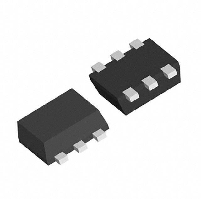
Since the packages for these ICs are DFN(PLP)1212-6, SOT-23-5, and SC-88A, high density mounting of the
ICs on board is possible.
FEATURES
• Supply Current ...................................................................... Typ. 0.8µA (R3134x27Ex, VDD=3.0V)
• Operating Voltage Range...................................................... 0.75V to 6.0V (Topt=25°C)
• Detector Threshold Range .................................................... 1.0V to 5.0V (0.1V steps)
Further, 2.32V, 2.63V, 2.93V, 3.08V, 4.38V, and
4.63V can be provided as standard.
• Detector Threshold Accuracy ................................................ ±1.8%
• Temperature-Drift Coefficient of Detector Threshold ............ Typ. ±100ppm/°C
• Built-in Delay Time Circuit ..................................................... Typ. 240ms
• Output Delay Time Accuracy................................................. ±15%
• Output Types ......................................................................... Nch Open Drain and CMOS
• Packages .............................................................................. DFN(PLP)1212-6, SC-88A, SOT-23-5
APPLICATIONS
•
•
•
•
•
•
CPU and Logic Circuit Reset
Battery Checker
Window Comparator
Wave Shaping Circuit
Battery Back-up Circuit
Power Failure Detector
1
�∗ R3134K (DFN(PLP)1212-6) and R3134Q (SC-88A) are the discontinued products as of March, 2016.
R3134x
BLOCK DIAGRAMS
Nch Open Drain Output (R3134xxxEA)
VDD
CMOS Output (R3134xxxEC)
MR
Delay
Circuit
VDD
MR
DOUT
Delay
Circuit
Vref
DOUT
Vref
GND
GND
SELECTION GUIDE
The package type, the detector threshold, the output type and the taping type for the ICs can be selected at
the users’ request.
Quantity per
Product Name
Package
Pb Free
Halogen Free
Reel
DFN(PLP)1212-6
5,000 pcs
Yes
Yes
R3134QxxE∗(y)-TR-FE
SC-88A
3,000 pcs
Yes
Yes
R3134NxxE∗(y)-TR-FE
SOT-23-5
3,000 pcs
Yes
Yes
R3134KxxE∗(y)-TR
xx : The detector threshold can be designated in the range from 1.0V(10) to 5.0V(50) in 0.1V steps.
y: If the detector threshold includes the 3rd digit, indicate the digit of 0.01V.
(Example) If the detector threshold is 2.63V, R3134x26E∗3-TR-x
∗ : Designation of Output Type
(A) Nch Open Drain
(C) CMOS
2
�∗ R3134K (DFN(PLP)1212-6) and R3134Q (SC-88A) are the discontinued products as of March, 2016.
R3134x
PIN CONFIGURATIONS
• DFN(PLP)1212-6
Top View
Bottom View
6
5
4
4
5
6
1
2
3
3
2
1
• SC-88A
5
• SOT-23-5
5
4
(mark side)
1
2
4
(mark side)
3
1
2
3
PIN DESCRIPTIONS
•
Pin No. Symbol
•
•
DFN(PLP)1212-6
Description
SC-88A
Pin No. Symbol
1
VDD
Input Pin
1
VDD
2
NC
No Connection
2
GND
3
GND
Ground Pin
3
MR
4
DOUT
4
DOUT
5
NC
No Connection
5
NC
6
MR
Manual Reset Input Pin∗
Output Pin
("L" at detection)
Description
Input Pin
Ground Pin
Manual Reset Input Pin∗
Output Pin
("L" at detection)
No Connection
SOT-23-5
Pin No. Symbol
Description
Output Pin
1
DOUT
2
VDD
3
GND
4
MR
Manual Reset Input Pin∗
5
NC
No Connection
("L" at detection)
Input Pin
Ground Pin
∗) MR pin is active at "L" input. Pulled up via 1MΩ (Typ.). If MR pin is not necessary, open this node, or connect
it to VDD.
3
�∗ R3134K (DFN(PLP)1212-6) and R3134Q (SC-88A) are the discontinued products as of March, 2016.
R3134x
ABSOLUTE MAXIMUM RATINGS
Symbol
VDD
VOUT
Item
Supply Voltage
Output Voltage (Nch Open Drain Output)
Rating
Unit
6.5
V
VSS−0.3 to 6.5
V
Output Voltage (CMOS Output)
VSS−0.3 to VDD+0.3
VMR
Input Voltage
VSS−0.3 to VDD+0.3
V
IOUT
Output Current
20
mA
Power Dissipation (DFN(PLP)1212-6)∗
400
Power Dissipation (SC-88A)∗
380
Power Dissipation (SOT-23-5)∗
420
Topt
Operating Temperature Range
−40 to 85
°C
Tstg
Storage Temperature Range
−55 to 125
°C
PD
mW
∗) For Power Dissipation, please refer to PACKAGE INFORMATION.
ABSOLUTE MAXIMUM RATINGS
Electronic and mechanical stress momentarily exceeded absolute maximum ratings may cause the
permanent damages and may degrade the life time and safety for both device and system using the device
in the field. The functional operation at or over these absolute maximum ratings is not assured.
4
�∗ R3134K (DFN(PLP)1212-6) and R3134Q (SC-88A) are the discontinued products as of March, 2016.
R3134x
ELECTRICAL CHARACTERISTICS
•
R3134x
The specification in
is checked and guaranteed by design engineering at −40°C ≤ Topt ≤ 85°C.
Topt=25°C
Symbol
Item
Conditions
Min.
VDET
×0.982
Typ.
Max.
VDET
×1.018
Unit
VDET
Detector Threshold
ISS1
Supply Current1
VDD=VDET−0.1V, IOUT=0A
2.0
µA
ISS2
Supply Current2
VDD=VDET+0.1V, IOUT=0A
2.0
µA
VDET < 1.6V
3.6
Supply Current3
VDD=6V,
IOUT=0A
1.6 ≤ VDET < 2.7V
3.0
2.7V ≤ VDET
2.5
ISS3
Topt=25°C
0.75
6.00
−40°C ≤ Topt ≤ 85°C
0.85
6.00
VDD
Operating Voltage
VOH
"H" Output Voltage
Refer to the following table
VOL
"L" Output Voltage
Refer to the following table
VIH
MR pin "H" Input Voltage
VDD ≥ VDET+0.1V
VIL
MR pin "L" Input Voltage
VDD ≥ VDET+0.1V
RMR
MR pin pull-up Resistance
Topt=25°C
Detector Threshold
Temperature Coefficient
−40°C ≤ Topt ≤ 85°C
treset
Output Delay Time for
detect ∗
VDD=VDET→ VDET−0.1V
tdelay
Output Delay Time for
release
VDD=0.8V→ VDET+1.0
∆VDET/
∆Topt
204
µA
V
V
0.75×VDD
0.5
V
1.0
0.2×VDD
V
4.0
MΩ
±100
ppm
/°C
15
µs
240
276
ms
∗) Guaranteed by design, not mass production tested.
RECOMMENDED OPERATING CONDITIONS (ELECTRICAL CHARACTERISTICS)
All of electronic equipment should be designed that the mounted semiconductor devices operate within the
recommended operating conditions. The semiconductor devices cannot operate normally over the
recommended operating conditions, even if when they are used over such conditions by momentary
electronic noise or surge. And the semiconductor devices may receive serious damage when they continue
to operate over the recommended operating conditions.
5
�∗ R3134K (DFN(PLP)1212-6) and R3134Q (SC-88A) are the discontinued products as of March, 2016.
R3134x
•
Topt=25°C
"H" Output Voltage (VOH) table
Products
R3134xxxEC
Detector Threshold
VDET (V)
"H" Output Voltage VOH (V)
Conditions
VDET < 1.2V
VDD=VDET+0.1V, IOH=50µA
1.2V ≤ VDET < 2.0V
VDD=VDET+0.1V, IOH=150µA
2.0V ≤ VDET < 3.1V
VDD=VDET+0.1V, IOH=500µA
3.1V ≤ VDET
VDD=VDET+0.1V, IOH=800µA
Min.
Typ.
Max.
0.8×VDD
VDET is a set value.
•
Products
R3134xxxEx
VDET is a set value.
6
Topt=25°C
"L" Output Voltage (VOL) table
"L" Output Voltage VOL (V)
Detector Threshold
VDET (V)
Conditions
VDET < 1.2V
VDD=VDET−0.1V, IOL=200µA
0.04
1.2V ≤ VDET < 2.0V
VDD=VDET−0.1V, IOL=750µA
0.06
2.0V ≤ VDET < 3.1V
VDD=VDET−0.1V, IOL=1.2mA
0.05
3.1V ≤ VDET
VDD=VDET−0.1V, IOL=3.2mA
0.06
Min.
Typ.
Max.
�∗ R3134K (DFN(PLP)1212-6) and R3134Q (SC-88A) are the discontinued products as of March, 2016.
R3134x
DETECTOR THRESHOLD SPECIFICATIONS BY PART NUMBER
•
R3134x
Operating Voltage
Part Number
VDD [V]
Conditions
R3134x23Ex2
R3134x26Ex3
R3134x29Ex3
R3134x30Ex8
R3134x43Ex8
R3134x46Ex3
R3134x10Ex
R3134x11Ex
R3134x12Ex
R3134x13Ex
R3134x14Ex
R3134x15Ex
R3134x16Ex
R3134x17Ex
R3134x18Ex
R3134x19Ex
R3134x20Ex
R3134x21Ex
R3134x22Ex
R3134x23Ex
R3134x24Ex
R3134x25Ex
R3134x26Ex
R3134x27Ex
R3134x28Ex
R3134x29Ex
R3134x30Ex
R3134x31Ex
R3134x32Ex
R3134x33Ex
R3134x34Ex
R3134x35Ex
R3134x36Ex
R3134x37Ex
R3134x38Ex
R3134x39Ex
R3134x40Ex
R3134x41Ex
R3134x42Ex
R3134x43Ex
R3134x44Ex
R3134x45Ex
R3134x46Ex
R3134x47Ex
R3134x48Ex
R3134x49Ex
R3134x50Ex
Detector Threshold
Topt=25°C
Topt=25°C
Min.
0.75
0.75
Conditions
−40°C ≤ Topt ≤ 85°C
−40°C ≤ Topt ≤ 85°C
VDET [V]
Min.
0.85
0.85
Supply Current 1
ISS1 [µA]
Min.
Typ.
Max.
2.278
2.583
2.877
3.025
4.301
4.547
0.982
1.080
1.178
1.277
1.375
1.473
1.571
1.669
1.768
1.866
1.964
2.062
2.160
2.259
2.357
2.455
2.553
2.651
2.750
2.848
2.946
3.044
3.142
3.241
3.339
3.437
3.535
3.633
3.732
3.830
3.928
4.026
4.124
4.223
4.321
4.419
4.517
4.615
4.714
4.812
4.910
2.320
2.630
2.930
3.080
4.380
4.630
1.000
1.100
1.200
1.300
1.400
1.500
1.600
1.700
1.800
1.900
2.000
2.100
2.200
2.300
2.400
2.500
2.600
2.700
2.800
2.900
3.000
3.100
3.200
3.300
3.400
3.500
3.600
3.700
3.800
3.900
4.000
4.100
4.200
4.300
4.400
4.500
4.600
4.700
4.800
4.900
5.000
2.362
2.677
2.983
3.135
4.459
4.713
1.018
1.120
1.222
1.323
1.425
1.527
1.629
1.731
1.832
1.934
2.036
2.138
2.240
2.341
2.443
2.545
2.647
2.749
2.850
2.952
3.054
3.156
3.258
3.359
3.461
3.563
3.665
3.767
3.868
3.970
4.072
4.174
4.276
4.377
4.479
4.581
4.683
4.785
4.886
4.988
5.090
Conditions
Typ.
Max.
0.8
VDD=VDET−0.1V
IOUT=0A
2.0
0.9
0.8
VDD=VDET−0.1V
IOUT=0A
2.0
0.9
7
�∗ R3134K (DFN(PLP)1212-6) and R3134Q (SC-88A) are the discontinued products as of March, 2016.
R3134x
Supply Current 2
Supply Current 3
ISS2 [µA]
Conditions
VDD=VDET+0.1V
IOUT=0A
Typ.
0.8
"H" Output Voltage
ISS3 [µA]
Max.
2.0
Conditions
VDD=6.0V
IOUT=0A
VOH [V]
Typ.
Max.
1.2
3.0
1.0
2.5
Conditions
VDD=VDET+0.1V
IOH=500µA
Min.
0.8×
VDD
VDD=VDET+0.1V
IOH=800µA
VDD=VDET+0.1V
IOH=50µA
3.6
1.4
VDD=VDET+0.1V
IOH=150µA
3.0
1.2
VDD=VDET+0.1V
IOH=500µA
VDD=VDET+0.1V
IOUT=0A
0.8
2.0
VDD=6.0V
IOUT=0A
0.8×
VDD
1.0
2.5
VDD=VDET+0.1V
IOH=800µA
0.8
8
�∗ R3134K (DFN(PLP)1212-6) and R3134Q (SC-88A) are the discontinued products as of March, 2016.
R3134x
Part Number
R3134x23Ex2
R3134x26Ex3
R3134x29Ex3
R3134x30Ex8
R3134x43Ex8
R3134x46Ex3
R3134x10Ex
R3134x11Ex
R3134x12Ex
R3134x13Ex
R3134x14Ex
R3134x15Ex
R3134x16Ex
R3134x17Ex
R3134x18Ex
R3134x19Ex
R3134x20Ex
R3134x21Ex
R3134x22Ex
R3134x23Ex
R3134x24Ex
R3134x25Ex
R3134x26Ex
R3134x27Ex
R3134x28Ex
R3134x29Ex
R3134x30Ex
R3134x31Ex
R3134x32Ex
R3134x33Ex
R3134x34Ex
R3134x35Ex
R3134x36Ex
R3134x37Ex
R3134x38Ex
R3134x39Ex
R3134x40Ex
R3134x41Ex
R3134x42Ex
R3134x43Ex
R3134x44Ex
R3134x45Ex
R3134x46Ex
R3134x47Ex
R3134x48Ex
R3134x49Ex
R3134x50Ex
"L" Output Voltage
MR pin "H" Input
Voltage
MR pin "L" Input
Voltage
MR pin pull-up resistance
VOL [V]
VIH [V]
VIL [V]
RMR [MΩ]
Conditions
Max.
VDD=VDET−0.1V
IOL=1.2mA
0.05
VDD=VDET−0.1V
IOL=3.2mA
0.06
VDD=VDET−0.1V
IOL=200µA
0.04
VDD=VDET−0.1V
IOL=750µA
0.06
VDD=VDET−0.1V
IOL=1.2mA
0.05
VDD=VDET−0.1V
IOL=3.2mA
Conditions
Min.
Conditions
Max.
Conditions
Min.
Typ.
Max.
VDD ≥ VDET+0.1
0.75×
VDD
VDD ≥ VDET+0.1
0.2×
VDD
Topt=25°C
0.5
1.0
4.0
VDD ≥ VDET+0.1
0.75×
VDD
VDD ≥ VDET+0.1
0.2×
VDD
Topt=25°C
0.5
1.0
4.0
0.06
9
�∗ R3134K (DFN(PLP)1212-6) and R3134Q (SC-88A) are the discontinued products as of March, 2016.
R3134x
10
Output Delay Time for Release
Detector Threshold
Temperature Coefficient
tdelay [ms]
∆VDET/∆Topt [ppm/°C]
Conditions
Min.
Typ.
Max.
Conditions
Typ.
VDD=0.8V→
VDET+1.0V
Topt=25°C
204
240
276
−40°C ≤ Topt ≤ 85°C
±100
VDD=0.8V→
VDET+1.0V
Topt=25°C
204
240
276
−40°C ≤ Topt ≤ 85°C
±100
�∗ R3134K (DFN(PLP)1212-6) and R3134Q (SC-88A) are the discontinued products as of March, 2016.
R3134x
TIMING CHART
Detector
Threshold
Power
VDET
Supply Minimum
(VDD) Operating Voltage
GND
Manual Reset
(VMR)
GND
Output Voltage
(VOUT)
GND
tdelay
tdelay
R3134x Operating Diagram
DEFINITION OF OUTPUT DELAY TIME
Output Delay Time (tdelay) is specified as follows:
1. In the case of Nch Open Drain Output:
The time interval from rising edge of VDD pulse 0.8V to VDET+1.0V to the time at which the output reaches
2.5V under the condition that the output pin (DOUT ) is pulled up to 5V through a 470kΩ resistor.
2. In the case of CMOS Output:
The time interval from rising edge of VDD pulse 0.8V to VDET+1.0V to the time at the output reaches
(VDET+1.0V)/2.
VDET+1.0V
Input Voltage
(VDD)
Input Voltage
(VDD)
VDET+1.0V
0.8V
GND
0.8V
GND
5.0V
Output Voltage
(VOUT)
2.5V
VDET+1.0V
Output Voltage
(VOUT)
(VDET+1.0V)/2
GND
GND
treset
tdelay
treset
Nch Open Drain Output
CMOS Output
(R3134xxxEA)
(R3134xxxEC)
tdelay
11
�∗ R3134K (DFN(PLP)1212-6) and R3134Q (SC-88A) are the discontinued products as of March, 2016.
R3134x
OPERATION
•
Operation of R3134xxxEA
VDD
Ra
DOUT pin should be pulled-up to
an external voltage level.
Comparator
Delay
Circuit
Vref
DOUT
Rb
Nch
GND
Block Diagram
1
2
3
Detector Threshold VDET A
=Released Voltage
4
5
B
Supply Voltage (VDD)
Minimum Operating VDDL
Voltage
GND
Pull-up Voltage
Output Voltage
(VOUT)
Detect
Delay Time
treset
Output
Delay Time
tdelay
GND
Operation Diagram
•
Explanation of operation
Step 1. The output voltage is equal to the pull-up voltage.
Step 2. At Point "A", Vref ≥ VDD×Rb/(Ra+Rb) is true, as a result, the output of comparator is reversed from "L" to
"H", therefore the output voltage becomes the GND level. The voltage level of Point A means a detector
threshold voltage (VDET).
Step 3. When the supply voltage is lower than the minimum operating voltage, the operation of the output
transistor becomes indefinite. The output voltage is equal to the pull-up voltage.
Step 4. The output voltage is equal to the GND level.
Step 5. At Point "B", Vref ≤ VDD×Rb/(Ra+Rb) is true, as a result, the output of comparator is reversed from "H" to
"L", then the output voltage is equal to the pull-up voltage. The voltage level of Point B means a released
voltage (VDET).
∗) There is no hysteresis range between the detector threshold and the released voltage.
12
�∗ R3134K (DFN(PLP)1212-6) and R3134Q (SC-88A) are the discontinued products as of March, 2016.
R3134x
•
Operation of R3134xxxEC
VDD
Ra
Pch
Comparator
Delay
Circuit
Vref
DOUT
Rb
Nch
GND
Block Diagram
1
2
3
Detector Threshold VDET A
=Released Voltage
4
5
B
Supply Voltage (VDD)
Minimum Operating VDDL
Voltage
GND
Output Voltage
(VOUT)
Detect
Delay Time
treset
Output
Delay Time
tdelay
GND
Operation Diagram
•
Explanation of operation
Step 1. The output voltage is equal to the supply voltage (VDD).
Step 2. At Point "A", Vref ≥ VDD×Rb/(Ra+Rb) is true, as a result, the output of comparator is reversed from "L" to
"H", therefore the output voltage becomes the GND level. The voltage level of Point A means a detector
threshold voltage (VDET).
Step 3. When the supply voltage is lower than the minimum operating voltage, the operation of the output
transistor becomes indefinite.
Step 4. The output voltage is equal to the GND level.
Step 5. At Point "B", Vref ≤ VDD×Rb/(Ra+Rb) is true, as a result, the output of comparator is reversed from "H" to
"L", then the output voltage is equal to the supply voltage (VDD). The voltage level of Point B means a
released voltage (VDET).
∗) There is no hysteresis range between the detector threshold and the released voltage.
13
�∗ R3134K (DFN(PLP)1212-6) and R3134Q (SC-88A) are the discontinued products as of March, 2016.
R3134x
Detector Operation vs. glitch input voltage to the VDD pin
When the IC is released and a large pulse (glitch) crosses the detector threshold is forced, the IC may not
maintain the released condition. The amplitude of the pulse (VDET-VDDmin) and the pulse width the IC can maintain
the released level is described in the graph as follows:
VIN Input Waveform
The graph above shows the condition for the maximum transient duration without generating a reset. If the
larger amplitude or larger pulse width noise than the graph may be on the VDD, the reset signal may be generated.
14
�∗ R3134K (DFN(PLP)1212-6) and R3134Q (SC-88A) are the discontinued products as of March, 2016.
R3134x
TEST CIRCUITS
ISS
5V
VDD
VDD
R3134x
Series
VIN
VIN
DOUT
R3134x
Series
MR
Supply Current Test Circuit
Detector Threshold Test Circuit
(Pull-up circuit is not necessary for CMOS Output type.)
VDD
MR
VDD
VOH
DOUT
GND
VIN
VOUT
DOUT
GND
GND
R3134x
Series
470kΩ
V
IOUT
MR
R3134x
Series
GND
VIN
"H" Output Voltage Test Circuit
DOUT
IOUT
V
VOL
"L" Output Voltage Test Circuit
(CMOS Output Type only)
ISS
5V
VDD
VIN
VMR
MR
R3134x
Series
470kΩ
DOUT
VOUT
GND
MR pin Input Voltage Test Circuit
(Pull-up circuit is not necessary for CMOS Output type.)
VDD
IMR
VIN
VMR
MR
R3134x
Series
GND
MR pin Pull-up Resistance Test Circuit
15
�∗ R3134K (DFN(PLP)1212-6) and R3134Q (SC-88A) are the discontinued products as of March, 2016.
R3134x
VDD
R3134x
Series
VIN
IOZ
DOUT
VDS
GND
Off Leakage Current Test Circuit
VDET+1.0V
Input Voltage
5V
VDD
1.0V
GND
Output Voltage
VIN
VDD
R3134x
Series
GND
50%
GND
tdelay
Output Delay Time Test Circuit
(Pull-up circuit is not necessary for CMOS Output type.)
16
DOUT
VOUT
�∗ R3134K (DFN(PLP)1212-6) and R3134Q (SC-88A) are the discontinued products as of March, 2016.
R3134x
TYPICAL CHARACTERISTICS
1) Supply Current vs. Input Voltage
R3134x10Ex
R3134x27Ex
R3134x16Ex
R3134x48Ex
2) Detector Threshold vs. Temperature
R3134x10Ex
R3134x16Ex
17
�∗ R3134K (DFN(PLP)1212-6) and R3134Q (SC-88A) are the discontinued products as of March, 2016.
R3134x
R3134x27Ex
R3134x48Ex
3) Nch Driver Output Current vs. VDS (Topt=25°C)
18
R3134x10Ex
R3134x16Ex
R3134x27Ex
R3134x48Ex
�∗ R3134K (DFN(PLP)1212-6) and R3134Q (SC-88A) are the discontinued products as of March, 2016.
R3134x
4) Nch Driver Output Current vs. Input Voltage
R3134x10Ex
R3134x16Ex
R3134x27Ex
R3134x48Ex
5) Pch Driver Output Current vs. VDS
R3134x10EC
R3134x16EC
19
�∗ R3134K (DFN(PLP)1212-6) and R3134Q (SC-88A) are the discontinued products as of March, 2016.
R3134x
R3134x27EC
R3134x48EC
6) Pch Driver Output Current vs. Input Voltage
20
R3134x10EC
R3134x16EC
R3134x27EC
R3134x48EC
�∗ R3134K (DFN(PLP)1212-6) and R3134Q (SC-88A) are the discontinued products as of March, 2016.
R3134x
7) Output Delay Time at Detection Mode vs. Temperature
R3134x10Ex
R3134x16Ex
R3134x27Ex
R3134x48Ex
8) Power-on Reset Delay Time vs. Temperature
R3134x10Ex
R3134x16Ex
21
�∗ R3134K (DFN(PLP)1212-6) and R3134Q (SC-88A) are the discontinued products as of March, 2016.
R3134x
R3134x27Ex
R3134x48Ex
TECHNICAL NOTES
When connecting resistors to the device’s input pin
When connecting a resistor (R1) to an input of this device, the input voltage decreases by [Device’s
Consumption Current] x [Resistance Value] only. And, the cross conduction current*1, which occurs when
changing from the detecting state to the release state, is decreased the input voltage by [Cross Conduction
Current] x [Resistance Value] only. And then, this device will enter the re-detecting state if the input voltage
reduction is larger than the difference between the detector voltage and the released voltage.
When the input resistance value is large and the VDD is gone up at mildly in the vicinity of the released voltage,
repeating the above operation may result in the occurrence of output.
As shown in Figure A/B, set R1 to become 100 kΩ or less as a guide, and connect CIN of 0.1 μF and more to
between the input pin and GND. Besides, make evaluations including temperature properties under the actual
usage condition, with using the evaluation board like this way. As a result, make sure that the cross conduction
current has no problem.
R1
R1
VDD
CIN
*2
Voltage
Detector
VDD
OUT pin
R2
CIN
*2
GND
Figure A
*1 In the CMOS output type, a charging current for OUT pin is included.
*2 Note the bias dependence of capacitors.
22
Voltage
Detector
GND
Figure B
OUT pin
�1. The products and the product specifications described in this document are subject to change or discontinuation of
production without notice for reasons such as improvement. Therefore, before deciding to use the products, please
refer to Ricoh sales representatives for the latest information thereon.
2. The materials in this document may not be copied or otherwise reproduced in whole or in part without prior written
consent of Ricoh.
3. Please be sure to take any necessary formalities under relevant laws or regulations before exporting or otherwise
taking out of your country the products or the technical information described herein.
4. The technical information described in this document shows typical characteristics of and example application circuits
for the products. The release of such information is not to be construed as a warranty of or a grant of license under
Ricoh's or any third party's intellectual property rights or any other rights.
5. The products listed in this document are intended and designed for use as general electronic components in standard
applications (office equipment, telecommunication equipment, measuring instruments, consumer electronic products,
amusement equipment etc.). Those customers intending to use a product in an application requiring extreme quality
and reliability, for example, in a highly specific application where the failure or misoperation of the product could result
in human injury or death (aircraft, spacevehicle, nuclear reactor control system, traffic control system, automotive and
transportation equipment, combustion equipment, safety devices, life support system etc.) should first contact us.
6. We are making our continuous effort to improve the quality and reliability of our products, but semiconductor products
are likely to fail with certain probability. In order to prevent any injury to persons or damages to property resulting from
such failure, customers should be careful enough to incorporate safety measures in their design, such as redundancy
feature, fire containment feature and fail-safe feature. We do not assume any liability or responsibility for any loss or
damage arising from misuse or inappropriate use of the products.
7. Anti-radiation design is not implemented in the products described in this document.
8. The X-ray exposure can influence functions and characteristics of the products. Confirm the product functions and
characteristics in the evaluation stage.
9. WLCSP products should be used in light shielded environments. The light exposure can influence functions and
characteristics of the products under operation or storage.
10. There can be variation in the marking when different AOI (Automated Optical Inspection) equipment is used. In the
case of recognizing the marking characteristic with AOI, please contact Ricoh sales or our distributor before attempting
to use AOI.
11. Please contact Ricoh sales representatives should you have any questions or comments concerning the products or
the technical information.
Halogen Free
Ricoh is committed to reducing the environmental loading materials in electrical devices
with a view to contributing to the protection of human health and the environment.
Ricoh has been providing RoHS compliant products since April 1, 2006 and Halogen-free products since
April 1, 2012.
https://www.e-devices.ricoh.co.jp/en/
Sales & Support Offices
Ricoh Electronic Devices Co., Ltd.
Shin-Yokohama Office (International Sales)
2-3, Shin-Yokohama 3-chome, Kohoku-ku, Yokohama-shi, Kanagawa, 222-8530, Japan
Phone: +81-50-3814-7687 Fax: +81-45-474-0074
Ricoh Americas Holdings, Inc.
675 Campbell Technology Parkway, Suite 200 Campbell, CA 95008, U.S.A.
Phone: +1-408-610-3105
Ricoh Europe (Netherlands) B.V.
Semiconductor Support Centre
Prof. W.H. Keesomlaan 1, 1183 DJ Amstelveen, The Netherlands
Phone: +31-20-5474-309
Ricoh International B.V. - German Branch
Semiconductor Sales and Support Centre
Oberrather Strasse 6, 40472 Düsseldorf, Germany
Phone: +49-211-6546-0
Ricoh Electronic Devices Korea Co., Ltd.
3F, Haesung Bldg, 504, Teheran-ro, Gangnam-gu, Seoul, 135-725, Korea
Phone: +82-2-2135-5700 Fax: +82-2-2051-5713
Ricoh Electronic Devices Shanghai Co., Ltd.
Room 403, No.2 Building, No.690 Bibo Road, Pu Dong New District, Shanghai 201203,
People's Republic of China
Phone: +86-21-5027-3200 Fax: +86-21-5027-3299
Ricoh Electronic Devices Shanghai Co., Ltd.
Shenzhen Branch
1205, Block D(Jinlong Building), Kingkey 100, Hongbao Road, Luohu District,
Shenzhen, China
Phone: +86-755-8348-7600 Ext 225
Ricoh Electronic Devices Co., Ltd.
Taipei office
Room 109, 10F-1, No.51, Hengyang Rd., Taipei City, Taiwan (R.O.C.)
Phone: +886-2-2313-1621/1622 Fax: +886-2-2313-1623
�


 工商网监
湘ICP备2023018690号
工商网监
湘ICP备2023018690号
